
Evolutionary Developments of DRAM Device Architecture
The first Dynamic Random-Access Memory(DRAM) device, based on the operation of Field Effect Transistors (FET), was invented by Robert Dennard of IBM in 1966. Then in 1970, Intel Corp. produced the first commercial DRAM device, the 1103. In the decades since the introduction of Intel’s 1103 DRAM device, DRAM device architecture has undergone continuous and gradual evolution. However, up until the mid-1990s, the evolutionary path of DRAM device architecture had been dominated by a single path devoted to high-capacity, low-cost commodity devices.
In recent years, the differing requirements placed on modern DRAM memory systems have strained the evolutionary development of modern DRAM devices. Consequently, the largely monolithic path of DRAM device architecture evolution has fractured into multiple evolutionary paths in recent years to respectively satisfy the varying system requirements of low cost, high bandwidth, low latency, and low power.
In previous chapters, basic structures of DRAM devices, common system configurations, abstract timing parameters, and abstract access protocols were described in detail. These chapters provide the foundation that enables the discussion in the rationale and capability of different DRAM devices. This chapter is devoted to the description and architectural evolution of different families of stand-alone DRAM devices.
12.1 DRAM Device Families
In the decades since the invention of the basic charge-storage DRAM circuit and the introduction of the first DRAM device, a myriad of DRAM devices, each with slightly different device architectures, has been developed to meet specific system requirements of low cost, low latency, high bandwidth, low power, or a reasonable combination thereof. In this chapter, the role of different DRAM devices is examined in context by classifying the different paths of the DRAM family tree illustrated in Figure 12.1.

12.1.1 Cost (Capacity), Latency, Bandwidth, and Power
The utility and cost effectiveness of commodity DRAM devices have allowed them to proliferate and become critical design components in large varieties of computer systems and computing devices. However, the specific requirements of different computer systems and computing devices have, in turn, forced DRAM device architectures to evolve and meet the wide spectrum of system requirements. Consequently, large numbers of DRAM devices that vary widely in their respective architecture, feature set, and performance characteristics now exist and occupy different market niches. To begin the difficult task of describing and comparing different DRAM devices and different device architectures, four simple metrics are used in this chapter to broadly evaluate all DRAM devices and classify them into one of the four general paths of the family of DRAM devices described in this section. The four metrics are cost (capacity), latency, bandwidth, and power.
As described previously, different DRAM devices have been designed and manufactured to target low cost, low latency, high bandwidth, low power, or a reasonable compromise thereof. However, the single overriding consideration that has greatly impacted and constrained the evolutionary developments of DRAM device architectures is the issue of cost. In the general sense, cost-focused DRAM devices strive for the lowest cost per bit, and in this chapter, the focus on the lowest cost per bit is equated to the focus on capacity. In the decades since the invention of the DRAM circuit, the vast majority of DRAM devices manufactured and sold are commodity DRAM devices focused on cost, and these DRAM devices are classified in this chapter as belonging in the Commodity path of the DRAM device family tree. The classification of the DRAM family tree in this chapter follows the evolutionary family tree illustrated in Figure 12.1. Figure 12.1 separates and classifies the myriad of DRAM devices into four evolutionary paths in the DRAM family tree: the Commodity path, the Low-Latency path, the High-Bandwidth path, and the Low-Power path. To facilitate the examination of the numerous DRAM devices in the Commodity path, the Commodity path is further separated into Historical-Commodity and Modern-Commodity sub-paths. Alternatively, DRAM devices that focus on providing fast random accesses are classified as belonging to the Low-Latency path of the DRAM device family tree. DRAM devices that focus on delivering the highest bandwidth are classified as belonging to the High-Bandwidth path. Finally, the near-commodity Graphics-Oriented GDDR devices and Alternative DRAM devices that had appeared along the way in the evolution of the DRAM family tree—yet do not readily belong in the primary paths of the DRAM family tree—are also examined in Sections 12.5 and 12.6.
12.2 Historical-Commodity DRAM Devices
As stated previously, the overriding factor that has driven and continues to drive the development of DRAM devices is the cost per storage bit. As a consequence of the singular focus on cost, nearly all legacy DRAM devices that existed prior to the emergence of Synchronous DRAM (SDRAM) devices are classified in this chapter as belonging in the Historical-Commodity path of the DRAM family tree. Specifically, the commodity DRAM device evolved from asynchronous to fast page mode (FPM) to extended data-out (EDO) to burst-mode EDO (BEDO) and then finally into synchronous (SDRAM). In this chapter, SDRAM and its direct descendants such as DDR SDRAM, DDR2 SDRAM, and DDR3 SDRAM devices are classified as belonging in the Modern-Commodity path of the DRAM family tree, and these devices are examined in Section 12.3.
In this section, DRAM devices that belong to the Historical-Commodity path of the DRAM family tree are selectively examined, and the selected devices are the Intel 1103 DRAM device, the asynchronous DRAM device, the FPM DRAM device, the EDO DRAM device, and the BEDO DRAM device. These selectively examined devices represent important milestones in the evolutionary path of historical-commodity DRAM devices. However, a large number of different DRAM devices were produced by various DRAM manufacturers in the time period between the appearance of Intel’s 1103 DRAM device and the BEDO DRAM device. Consequently, it is important to note that while the DRAM devices selectively examined in this section illustrate well the gradual evolution of commodity DRAM devices from the early 1970s to the late 1990s, the few illustrated devices do not represent all of the DRAM devices and evolutionary attempts in that time period.
In the evolution of DRAM device architecture from Intel’s 1103 DRAM device to the BEDO DRAM device, the changes to the DRAM device have largely been structural in nature and relatively minor in terms of implementation cost; yet device functionality and throughput have increased significantly in each successive generation of DRAM devices. In the following section, the general description of the Historical-Commodity path of the DRAM family tree begins with a cursory examination of Intel’s 1103 DRAM device.
12.2.1 The Intel 1103
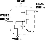
The first commercially successful DRAM device, the 1103, was introduced by Intel in 1971. Due to its relatively low cost, the 1103 gained wide acceptance and rapidly replaced magnetic core memory in many different applications. Figure 12.3 shows the package pin configuration of the 1103, and it shows that this device was packaged in a low-cost, 18-pin, plastic dual in-line package. The 1103 had a row cycle time of 580 ns and a random access time of 300 ns. The 1103 also had a data retention time that was guaranteed to be longer than 2 ms; as long as each cell was refreshed at least once every 2 ms, data integrity was guaranteed. Differing from DRAM devices that followed it in subsequent years, the 1103 also had some interesting features such as unidirectional data input and output. The unidirectional input and output gave the early DRAM devices such as the 1103 (up to FPM devices) an interesting capability—an atomic read-modify-write cycle. That is, as the DRAM device drives data out of the output, the memory controller can hold the address on the address bus. Then, the controller can read, process, and immediately write data back through the input to the same address—something not practical in later DRAM devices with bidirectional data busses. Also, the 1103 used dedicated pins for row and column addresses, while later devices typically multiplexed row and column addresses over a single set of address pins. Moreover, the 1103 was a rudimentary device in terms of power supply requirements. Unlike the more modern DRAM devices, the 1103 required separate power supplies to properly bias the transistors. Finally, one feature that differentiated the 1103 from later DRAM devices was that it utilized the 3 transistor, 1 capacitor (3T1C) structure as the basic storage cell. Due to the 3T1C cell structure in the 1103 illustrated in Figure 12.2, data read-out from the 1103 is nondestructive. Consequently, data does not need to be restored into the DRAM cell immediately after it is read out.

In comparison to the myriad of DRAM devices that followed it, Intel’s 1103 DRAM device was a rudimentary device that contained little more than address decoders and an array of 1024 DRAM cells. Common structures that were found in later devices, such as integrated address latches and sense amplifiers, were not present in the 1103. Consequently, a memory system that utilized the 1103 required more external circuitry than later devices. Figure 12.4 illustrates the structural block diagram of a memory system that utilizes the 1103.1 The figure shows that several important external circuits are needed to create a memory system based on the 1103. First, external voltage level shifters were needed to interface TTL devices to the MOS signal levels of the 1103. Second, the 1103 memory system required a significant amount of external logic to perform a simple read or write. Finally, the memory system used external sense amplifiers to resolve the stored data value from an 1103 DRAM device.

12.2.2 Asynchronous DRAM Devices
In the 1970s, subsequent to the introduction of Intel’s 1103 DRAM device, many other DRAM devices were produced by Intel and other DRAM manufacturers. These DRAM devices were not standardized, and each DRAM device was unique in some way, containing subtle improvements from the previous generation of DRAM devices. For example, subsequent to the 1103, Intel introduced the 2104 DRAM device that multiplexed the row address and the column address over the same address bus, the 2116 DRAM device that was Intel’s first 16-kbit DRAM device, and the 2118 DRAM device that was the first DRAM device to use a single 5-V power supply.
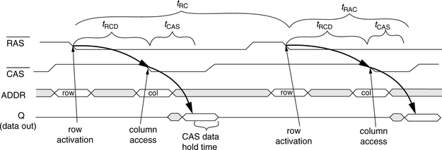
Other early DRAMs were sometimes clocked, where the DRAM commands were driven by a periodic clock signal. However, by the mid-1970s, DRAM device interfaces moved away from the clock-driven interface and moved to an Asynchronous command–data timing interface. These Asynchronous DRAM devices, like the clocked versions before them, require that every single access go through separate row activation and column access steps. Even if the microprocessor wants to request data contained in the same row that it previously requested, the entire row activation and column access process must be repeated. Figure 12.5 illustrates the timing for an asynchronous DRAM device. The figure shows that in the early asynchronous DRAM device, a row-activation command and a column-access command are needed to read data from the DRAM device, and two entire row cycles are needed to move data to or from any two addresses.
12.2.3 Page Mode and Fast Page Mode DRAM (FPM DRAM)
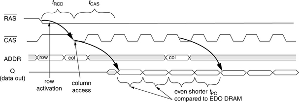
Since the introduction of Intel’s 1103 DRAM device, each successive DRAM device has introduced new features to improve upon previous DRAM devices. One important feature that greatly improved DRAM device performance and was found in all later DRAM devices is page mode operation. In page mode operation, an entire row (page) of data is held by an array of sense amplifiers integrated into the DRAM device, and multiple column accesses to data in the same row can occur without having to suffer the latency of another row access. Page mode operation in DRAM devices improves system performance by taking advantage of the spatial locality present in the memory-access patterns of typical application programs. Page mode operation was not possible in the earliest DRAM devices due to the fact that the sense amplifiers were located off-chip. However, this mode of operation was enabled by the integration of sense amplifiers into the DRAM device, and data for an entire row could be sensed and buffered by the array of integrated sense amplifiers in parallel. Page mode permitted fast column accesses, and FPM improved the timing of the column access by allowing the column address buffers to remain open and active for as long as the row address strobe signal was held low. In this manner, the column addresses could be sent through the column address buffer and decoded before the column address strobe signal was asserted by the memory controller. Consequently, FPM was introduced into many 64-kbit DRAM devices in the early 1980s. FPM DRAM remained as the mainstream commodity memory well into the 1990s until it was replaced, in part, by EDO DRAM and finally entirely by Synchronous DRAM (SDRAM) in the late 1990s.
Figure 12.6 illustrates the organization and structure of a 64-Mbit FPM DRAM device with a 16-bit-wide bidirectional data bus. The FPM DRAM device illustrated in Figure 12.6 is a relatively modern DRAM device with a bidirectional data bus, while early generations of FPM DRAM devices typically had separate and unidirectional data input and output pins. Internally, the DRAM storage cells in the FPM DRAM device in Figure 12.6 are organized as 4096 rows, 1024 columns per row, and 16 bits of data per column. In this device, each time a row access occurs, the row address is placed on the address bus, and the row address strobe (RAS) is asserted by an external memory controller. Inside the DRAM device, the address on the address bus is buffered by the row address buffer and then sent to the row decoder. The row address decoder then accepts the row address and selects 1 of 4096 rows of storage cells. The data values contained in the selected row of storage cells are then sensed and kept active by the array of sense amplifiers. Each row of DRAM cells in the illustrated FPM DRAM device consists of 1024 columns, and each column is 16 bits wide. That is, a 16-bit-wide column is the basic addressable unit of memory in this device, and each column access that follows the row access would read or write 16 bits of data from the same row of DRAM. The FPM DRAM device illustrated in Figure 12.6 does allow each 8-bit half of the 16-bit column to be accessed independently through the use of separate column access strobe high (CASH) and column access strobe low (CASL) signals. In FPM DRAM devices, column access commands are handled in a similar manner as the row access commands. For a column access command, the memory controller places the column address on the address bus and then asserts the appropriate CAS signals. Internally, the DRAM chip takes the column address, decodes it, and selects 1 column out of 1024 columns. The data for that column is then placed onto the data bus by the DRAM device in the case of an ordinary column read command or overwritten with data from the memory controller depending on the write enable (WE) signal.

Figure 12.7 illustrates the timing for page mode read commands in an FPM device. The figure shows that once a row is activated by holding the ![]() signal low, multiple column accesses can be used to retrieve spatially adjacent data from the same DRAM row with the timing of tPC, the page mode cycle time. Figure 12.7 also shows that the output data valid time period is implicitly controlled by the timing of the
signal low, multiple column accesses can be used to retrieve spatially adjacent data from the same DRAM row with the timing of tPC, the page mode cycle time. Figure 12.7 also shows that the output data valid time period is implicitly controlled by the timing of the ![]() signal. That is, the DRAM device will hold the value of the read data out for some period of time after
signal. That is, the DRAM device will hold the value of the read data out for some period of time after ![]() goes high. The DRAM device then prepares for a subsequent column-access command without an intervening precharge command or row-access command.
goes high. The DRAM device then prepares for a subsequent column-access command without an intervening precharge command or row-access command.
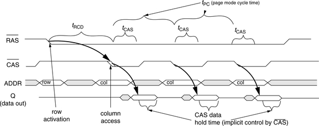
In FPM DRAM devices, the page mode cycle time can be as short as one-third of the row cycle time. Consequently, (fast) page mode operation increased DRAM device bandwidth for spatially adjacent data by as much as three times that of a comparable generation asynchronous DRAM device without page mode operation.
12.2.4 Extended Data-Out (EDO) and Burst Extended Data-Out (BEDO) Devices
FPM DRAM devices were highly popular and proliferated into many different applications in the 1980s and the first half of the 1990s. Then, in the mid-1990s, EDO, a new type of DRAM device, was introduced into the market and achieved some degree of success in replacing FPM DRAM devices in mainstream personal computers. The EDO DRAM device added a new output enable (![]() ) signal and allowed the DRAM device to hand over control of the output buffer from the
) signal and allowed the DRAM device to hand over control of the output buffer from the ![]() signal to the
signal to the ![]() signal. Consequently, read data on the output of the DRAM device can remain valid for a longer time after the
signal. Consequently, read data on the output of the DRAM device can remain valid for a longer time after the ![]() signal is driven high, thus the name “extended data-out.”
signal is driven high, thus the name “extended data-out.”
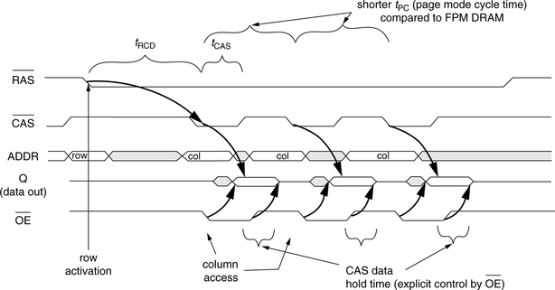
Figure 12.8 gives the timing for three column read commands in an EDO DRAM device. The figure shows that the explicit control of the output data means that the ![]() signal can be cycled around faster in an EDO DRAM device as compared to a FPM DRAM device, without impacting CAS data hold time. Consequently, EDO devices can achieve better (shorter) page mode cycle time, leading to higher device bandwidth when compared to FPM DRAM devices of the same process generation.
signal can be cycled around faster in an EDO DRAM device as compared to a FPM DRAM device, without impacting CAS data hold time. Consequently, EDO devices can achieve better (shorter) page mode cycle time, leading to higher device bandwidth when compared to FPM DRAM devices of the same process generation.
The EDO DRAM device achieved some success in replacing FPM DRAM devices in some markets, particularly the personal computer market. The higher bandwidth offered by the EDO DRAM device was welcomed by system design engineers and architects, as faster processors drove the need for higher memory bandwidth. However, the EDO DRAM device was unable to fully satisfy the demand for higher memory bandwidth, and DRAM engineers began to seek an evolutionary path beyond the EDO DRAM device.
The BEDO DRAM device builds on EDO DRAM by adding the concept of “bursting” contiguous blocks of data from an activated row each time a new column address is sent to the DRAM device. Figure 12.9 illustrates the timing of several column access commands for a BEDO DRAM device. The figure shows that the row activation command is given to the BEDO device by driving the ![]() signal low. The column access command in the BEDO device is then initiated by driving the
signal low. The column access command in the BEDO device is then initiated by driving the ![]() signal low, and the address of the column access command is latched in at that time. Figure 12.9 shows that unlike the DRAM devices that preceded it, the BEDO DRAM device then internally generates four consecutive column addresses and places the data for those columns onto the data bus with each falling edge on the
signal low, and the address of the column access command is latched in at that time. Figure 12.9 shows that unlike the DRAM devices that preceded it, the BEDO DRAM device then internally generates four consecutive column addresses and places the data for those columns onto the data bus with each falling edge on the ![]() signal. By eliminating the need to send successive column addresses over the bus to drive a burst of data in response to each microprocessor request, the BEDO device eliminates a significant amount of timing uncertainty between successive addresses, thereby further decreasing the page mode cycle time that correlates to increasing DRAM device bandwidth.
signal. By eliminating the need to send successive column addresses over the bus to drive a burst of data in response to each microprocessor request, the BEDO device eliminates a significant amount of timing uncertainty between successive addresses, thereby further decreasing the page mode cycle time that correlates to increasing DRAM device bandwidth.
12.3 Modern-Commodity DRAM Devices
The nature of the commodity DRAM business means that any proposed change to the DRAM device must incur relatively low circuit overhead for the change to be acceptable to DRAM device manufacturers. Consequently, changes to DRAM devices are often evolutionary (low die cost) rather than revolutionary (high die cost). For example, the circuit overhead for an EDO DRAM device over that of an FPM DRAM device was minimal, and the evolutionary step required only a subtle change in protocol. However, owing to the convergence of factors such as the push to attain higher device bandwidth and more functionality from the DRAM device, DRAM manufacturers and systems manufacturers gathered through the Joint Electron Device Engineering Council (JEDEC) and collectively defined a new DRAM device, the SDRAM device. Compared to the EDO DRAM device that preceded it, the SDRAM device contained many new features that separated it distinctly from DRAM devices that preceded it. In this manner, the SDRAM device represents a break in the commodity path of the DRAM family tree and separates the Modern-Commodity DRAM devices from the Historical-Commodity DRAM devices.
The SDRAM device proved to be a highly successful DRAM device that proliferated into many different applications. The SDRAM device also became the basis for many different DRAM devices that followed it. The device architecture of commodity DRAM devices such as the Dual Data Rate (DDR) SDRAM, the Dual Data Rate II (DDR2) SDRAM, and Dual Data Rate III (DDR3) SDRAM is the direct descendant of the SDRAM device architecture. The venerable SDRAM device can also claim as its descendant, directly or indirectly, DRAM devices such as the Graphics DDR (GDDR) SDRAM, Graphics DDR2 (GDDR2) SDRAM, Graphics DDR3 (GDDR3) SDRAM, Enhanced SDRAM (ESDRAM), and Virtual Channel SDRAM (VCDRAM), as well as Mobile SDRAM and Mobile DDR SDRAM. In this section, the evolutionary development for modern-commodity DRAM devices from SDRAM to DDR3 SDRAM devices are described and examined in detail.
12.3.1 Synchronous DRAM (SDRAM)
The SDRAM device is the first device in a line of modern-commodity DRAM devices. The SDRAM device represented a significant departure from the DRAM devices that preceded it. In particular, SDRAM devices differ from previous generations of FPM and EDO DRAM devices in three significant ways: the SDRAM device has a synchronous device interface, all SDRAM devices contain multiple internal banks, and the SDRAM device is programmable.
DRAM devices are controlled by memory controllers optimized for specific systems. In the case of FPM and EDO DRAM devices used in modern computer systems, the memory controller typically operated at specific, fixed frequencies to interface with other components of the system. The asynchronous nature of FPM and EDO devices—that can, in theory, enable different controller and system designs to aggressively extract performance from different DRAM devices with different timing parameters—was more of a hindrance than an asset in the design of high volume and relatively high-performance memory systems. Consequently, computer manufacturers pushed to place a synchronous interface on the DRAM device that also operated at frequencies commonly found in the computer systems of that era, resulting in the SDRAM device.
In FPM and EDO DRAM devices, the ![]() and
and ![]() signals from the memory controller directly control latches internal to the DRAM device, and these signals can arrive at the DRAM device’s pins at any time. The DRAM devices then respond to the
signals from the memory controller directly control latches internal to the DRAM device, and these signals can arrive at the DRAM device’s pins at any time. The DRAM devices then respond to the ![]() and
and ![]() signals at the best possible speed that they are inherently capable of. In SDRAM devices, the
signals at the best possible speed that they are inherently capable of. In SDRAM devices, the ![]() and
and ![]() signal names were retained for signals on the command bus that transmits commands, but these specific signals no longer control latches that are internal to the DRAM device. Rather, the signals deliver commands on the command bus of the SDRAM device, and the commands are only acted upon by the control logic of the SDRAM device at the falling edge of the clock signal. In this manner, the operation of the state machine in the DRAM device moved from the memory controller into the DRAM device, enabling features such as programmability and multi-bank operation.
signal names were retained for signals on the command bus that transmits commands, but these specific signals no longer control latches that are internal to the DRAM device. Rather, the signals deliver commands on the command bus of the SDRAM device, and the commands are only acted upon by the control logic of the SDRAM device at the falling edge of the clock signal. In this manner, the operation of the state machine in the DRAM device moved from the memory controller into the DRAM device, enabling features such as programmability and multi-bank operation.
The second feature that significantly differentiated the SDRAM device from FPM and EDO devices that preceded it was that the SDRAM device contained multiple banks internally. The presence of multiple, independent banks in each SDRAM device means that while one bank is busy with a row activation command or a precharge command, the memory controller can send a row access command to initiate row activation in a different bank or can send a column access command to a different open bank. The multi-bank architecture of the SDRAM device means that multiple memory requests can be pipelined to different banks of a single SDRAM device. The first-generation 16-Mbit SDRAM device contained only 2 banks of independent DRAM arrays, but higher capacity SDRAM devices contained 4 independent banks in each device.
The SDRAM device also contains additional functionalities such as a column-access-and-precharge command. These functionalities along with the programmable state machine and multiple banks of sense amplifiers mean that the SDRAM device contains significant circuit overhead compared to FPM and EDO DRAM devices of the same capacity and process generation. However, since the circuit overhead was relatively constant and independent of device capacity, the die size overhead of the additional circuitry became less of an issue with larger device capacities. Consequently, the relatively low delta in manufacturing costs in combination with demonstrable performance benefits enabled 100-MHz, 64-Mbit SDRAM devices to take over from FPM and EDO devices as the mainstream commodity DRAM device.
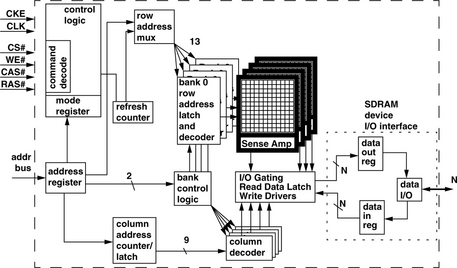
Figure 12.10 shows a block diagram of an SDRAM device. The figure shows that the SDRAM device, unlike the FPM DRAM device in Figure 12.6, has 4 banks of DRAM arrays internally, each with its own array of sense amplifiers. Similar to the FPM device, the SDRAM device contains separate address registers that are used to control dataflow on the SDRAM device. In case of a row access command, the address from the address register is forwarded to the row address latch and decoder, and that address is used to activate the selected wordline. Data is then discharged onto the bitlines, and the sense amplifiers array senses, amplifies, and holds the data for subsequent column accesses. In the case of a column read command, the data is sent through multiple levels of multiplexors, then through the I/O gating structure out to the data bus, and eventually driven into the memory controller. In the case of a column write command, the memory controller places data on the data bus, and the SDRAM device then latches the data in the data in register, drives the data through the I/O gating structure, and overwrites data in the sense amplifier arrays; the sense amplifiers, in turn, drive the new data values into the DRAM cells through the open access transistors.
In an SDRAM device, commands are decoded on the rising edge of the clock signal (CLK) if the chip-select line (CS#) is active. The command is asserted by the DRAM controller on the command bus, which consists of the write enable (WE#), column access (CAS#), and row access (RAS#) signal lines. Although the signal lines have function-specific names, they essentially form a command bus, allowing the SDRAM device to recognize more commands without the use of additional signal lines. Table 12.1 shows the command set of the SDRAM device and the signal combinations on the command bus. The table shows that as long as CS# is not selected, the SDRAM device ignores the signals on the command bus. In the case where CS# is active on the rising edge of the clock, the SDRAM device then decodes the combination of control signals on the command bus. For example, the SDRAM device recognizes that the combination of an active low voltage value on RAS#, an interactive high voltage value on CAS#, and an inactive high voltage value on WE# as a row activation command and begins the row activation process on the selected bank, using the row address as provided on the address bus.
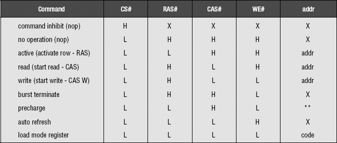
A different combination of signal values on the command bus allows the SDRAM device to load in new values for the mode register. That is, in the case where CS#, RAS#, CAS#, and WE# are all active on the rising edge of the clock signal, the SDRAM device decodes the load mode register command and loads the mode register from values presented on the address bus.
The third feature in an SDRAM device that differentiates it from previous DRAM devices is that the SDRAM device contains a programmable mode register, and the behavior of the DRAM device depends on the values contained in the various fields of the mode register. The presence of the mode register means that the SDRAM device can exhibit different behaviors in response to a given command. Specifically, the mode register in an SDRAM device allows it to have programmable CAS latency, programmable burst length, and programmable burst order.
Figure 12.11 shows that in an SDRAM device, the mode register contains three fields: CAS latency, burst type, and burst length. Depending on the value of the CAS latency field in the mode register, the DRAM device returns data two or three cycles after the assertion of the column read command. The value of the burst type determines the ordering of how the SDRAM device returns data, and the burst length field determines the number of columns that an SDRAM device will return to the memory controller with a single column read command. SDRAM devices can be programmed to return 1, 2, 4, or 8 columns or an entire row. Direct RDRAM devices and DDRx SDRAM devices contain more mode registers that control an ever-larger set of programmable operations, including, but not limited to, different operating modes for power conservation, electrical termination calibration modes, self-test modes, and write recovery duration.
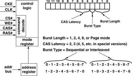
To execute a given command, the control logic block on the SDRAM device accepts commands sent on the command bus from the memory controller. Then, depending on the type of command and values contained in the respective fields of the mode register, the SDRAM device performs specific sequences of operations on successive clock cycles without requiring clock-by-clock control from the memory controller. For example, in the case of the column-read-and-precharge command, the SDRAM device accepts the command, and then, depending on the value programmed into the mode register, the SDRAM device begins to return data two or three clock cycles after the command was asserted on the command bus. The burst length and burst order of the single column access command also depends on the value programmed in the mode register. Then, the SDRAM device automatically precharges the DRAM bank after the column read command completes.
SDRAM-Access Protocol
Figure 12.12 illustrates some basic concepts of data access to an SDRAM memory system. The figure shows a total of three commands: a row activation command to bank i of rank n, followed by a column read access command to the same bank, followed by another column read access command to an open bank in a different rank. Figure 12.12 shows that the interface of the SDRAM memory system presents the memory system as a synchronous state machine that responds to commands issued from the memory controller. Specifically, Figure 12.12 shows that a row activation is started in an SDRAM device by the device latching the command and addresses on the rising edge of the clock signal. The SDRAM device then decodes the command and transitions the state machine on the DRAM device that is appropriate to the specific command received. In Figure 12.12, two cycles after the row activation command, the row-column delay time is satisfied, and the row is then assumed by the memory controller to be open. The memory controller then places the column read access command on the command bus, and tCAS time later, the SDRAM device begins to return data from the just-opened row to the memory controller. In Figure 12.12, the SDRAM devices are programmed to return four consecutive columns of data for each column access command, so four consecutive columns of data are placed onto the data bus by the DRAM device without further interaction from the memory controller. Finally, Figure 12.12 subtly illustrates that the synchronous interface of the SDRAM memory system is only a convenient illusion. For the case of two column read commands to different ranks, the change in the bus master of the data bus on back-to-back clock cycles leads to some minor uncertainty on the timing.

Die Photo and a TSOP Package
Figure 12.13 shows the die photograph of a 256-Mbit SDRAM device from Micron. In the figure, much of the surface area of the silicon die is dominated by the regular structures of the DRAM arrays.

In this case, roughly 70% of the silicon surface is used by the DRAM arrays, and the rest of the area is taken up by I/O pads, sense amplifiers, decoders, and the minimal control logic. The SDRAM device shown in Figure 12.13 is manufactured on a DRAM-optimized, 0.11-mm process with three layers of metal interconnects and six layers of polysilicon. The die size of the SDRAM device is approximately 45 mm2.
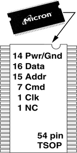
SDRAM devices are packaged in a low-cost Thin, Small Outline Package (TSOP). Figure 12.14 shows a 54-pin TSOP for an SDRAM device with a 16-bit-wide data bus. In a x16 SDRAM device, 14 pins on the 54-pin TSOP are used for power and ground, 16 pins are used for the data bus, 15 pins are used for the address bus, 7 pins are used for the command bus, and 1 pin is used for the clock signal.
DRAM Standardization and Qualification Processes
In April 1998, Intel Corp. introduced a new system controller that was the first controller to operate the SDRAM memory system at 100 MHz. Prior to the rollout of the 440BX AGPset, engineers at Intel discovered that memory modules manufactured by different module manufacturers, possibly utilizing different DRAM devices from different manufacturers, may not inter-operate in a seamless manner when placed into the same SDRAM memory system despite the fact that each module individually meets technical requirements for 100-MHz operation according to JEDEC standards specification. To ensure the success of the 440BX system controller chipset and the associated Pentium II processor platform, Intel Corp., in conjunction with DRAM device, DRAM module, and system manufacturers, adopted a more stringent set of standards for 100-MHz SDRAM memory. This set of stringent requirements for SDRAM memory to operate at 100 MHz was referred to as the PC100 standard.
The PC100 SDRAM standard ensured module inter-operability by further decreasing the allowable timing margins on the chip and module interface. The decreased timing margins placed more stringent requirements on SDRAM device and SDRAM memory module manufacturers. In an effort to alleviate the demand placed on these manufacturers, Intel began to provide reference designs of SDRAM memory modules complete with bills of materials that specified prequalified SDRAM parts, schematics that illustrated connection points on a memory module, and Gerber files that specified the connections within the PCB layers of a memory module, as well as the values and placement of resistors and capacitors on a memory module. The reference design approach reduced the burden placed on memory module manufacturers and allowed the PC100 standard to proliferate. Consequently, PC100 SDRAM memory modules quickly gained popularity as end-users were assured of high performance and trouble-free memory system configuration, regardless of configuration and manufacturer of the DRAM device or modules.
Subsequent to the PC100 standardization effort, Intel attempted to shift industry memory system architecture to Direct RDRAM. Consequently, Intel did not drive the 133-MHz PC133 standardization effort. Nevertheless, the qualification path set down by Intel to ensure compatibility between different manufacturers was used to drive subsequent standard qualification efforts for faster SDRAM and DDRx memory systems. Currently, the module standardization effort to ensure trouble-free inter-oper-ability resides in a subcomittee within JEDEC.
12.3.2 Double Data Rate SDRAM (DDR SDRAM)
The Double Data Rate (DDR) Synchronous DRAM device evolved from, and subsequently replaced, the SDRAM device as the mainstream commodity DRAM device. Consequently, DDR SDRAM device architecture closely resembles SDRAM device architecture. The primary difference between DDR SDRAM device architecture and the SDRAM device architecture is that the SDRAM device operates the data bus at the same data rate as the address and command busses, while the DDR SDRAM device operates the data bus at twice the data rate of the address and command busses. The reason that the data bus of the DDR SDRAM device operates at twice the data rate of the address and command busses is that signal lines on the data bus of the traditional SDRAM memory system topology are more lightly loaded than signal lines on the address and command busses. Figure 12.15 shows the general topology of the SDRAM memory system where there are N ranks of DRAM devices in the memory system with M ranks of DRAM devices per rank. In the topology shown in Figure 12.15, each pin on the address and command bus may drive as many as N * M loads, whereas the pins on the data bus are limited to the maximum of N loads. Consequently, the data bus can switch states at a much higher rate as compared to the address and command busses. DDR SDRAM devices are architected to take advantage of the imbalance in loading characteristics and operate the data bus at twice the data rate as the command and address busses.

FIGURE 12.15 SDRAM memory system topology shows uneven loading on the different busses. Electrical loading on the address bus is much heavier than on the data bus.
DDR SDRAM-Access Protocol
Figure 12.16 illustrates basic concepts of data access to a DDR SDRAM memory system. A total of three commands are shown: a row activation command to bank i of rank n, followed by a column read access command to the same bank, followed by another column read access command to an open bank in a different rank. Figure 12.16 shows that data transfer occurs at twice the rate on the data bus as compared to the address and command bus. Figure 12.16 also shows that the DDR SDRAM memory system uses the data strobe signal (DQS), a signal not found in previous-generation SDRAM devices, to provide a source-synchronous timing reference signal between the source and the destination. In DDR SDRAM devices, the DQS signal is controlled by the device that sends the data on the data bus. In the case of a read command, the DQS signal is used by the DRAM device to indicate the timing of read data delivery to the memory controller. In the case of a write command, the DQS signal is used by the memory controller to indicate the timing of write data delivery from the memory controller to the DRAM device.
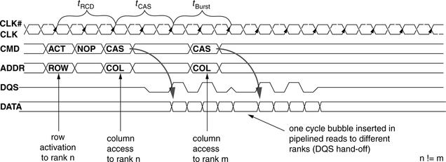
The timing diagram in Figure 12.16 shows a one-cycle bubble between data bursts from different ranks of DRAM devices. The one-cycle bubble exists because the DQS signal is a shared signal used by all data sources in the memory system. Consequently, one idle cycle is needed for one bus master to hand off control of the DQS signal line to another bus master, and the one-cycle bubble appears on the data bus as a natural result.
DDR SDRAM I/O Interface
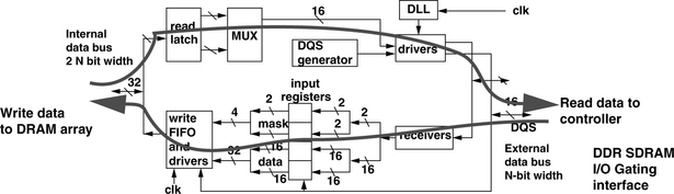
Figure 12.17 presents a block diagram view of the DDR SDRAM device I/O interface. As Figure 12.16 illustrates, DDR SDRAM memory systems transfer data on both edges of the DQS strobe signal. However, despite the increase in the rate of data transfer on the device interface, the rate of internal data transfer in the DDR SDRAM device is not similarly increased. Instead, in DDR SDRAM devices, the rate of data transfer is internally halved so that data movement occurs internally at twice the width, but half the rate of the device interface. DRAM device manufacturers have adopted the terminology of M-bit prefetch to describe the data rate multiplication architecture, where M represents the multiplication factor between the DRAM device’s internal width of data movement and the width of the data bus on the device interface. In this nomenclature, DDR SDRAM devices are said to have a 2-bit prefetch architecture where 2 * N bits are moved internally at rate Y, but the DDR SDRAM device provides an N-bit-wide interface to the memory system that moves data at rate 2 * Y.

Aside from the difference in the I/O interface of the DRAM device, DDR SDRAM device architecture is otherwise identical to SDRAM device architecture. Consequently, some DRAM manufacturers created unified designs that can be bonded out as a DDR SDRAM device of data width X or an SDRAM device of data width 2 * X. These unified designs allowed these manufacturers to quickly shift wafer allocations to meet shifting market demands. However, these unified designs typically cost several percentage points of die overhead, so their use was limited to the transitional period between SDRAM and DDR SDRAM devices.
Series Stub Terminated Signaling Protocol
Aside from the changes to the I/O architecture of the DRAM device, the signaling protocol used by the DDR SDRAM device also differed from the signaling protocol used by the SDRAM device. The signaling protocol used in DDR SDRAM devices had to meet two conditions: better signal integrity to achieve the higher data rate and a signaling protocol that would still permit the DRAM device core and the DRAM device interface to share a common, yet lower voltage level. The 2.5-V Series Stub Terminated Logic (SSTL-2) signaling protocol met the requirement for DRAM manufacturers to simultaneously achieve the higher signaling rates found in DDR SDRAM memory systems and to lower the device voltage from the 3.3 V used by SDRAM devices to 2.5 V. Consequently, SSTL-2 is used in all DDR SDRAM devices.
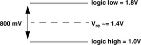
Figure 12.18 illustrates the idealized signal input and output characteristics for an SSTL-2 inverter. The figure shows that SSTL-2 differs from Low-Voltage Transistor-Transistor Logic (LVTTL) in that SSTL-2 uses a common reference voltage Vref to differentiate between a logically high voltage state and a logically low voltage state. The use of the common voltage reference enables SSTL-2 devices to enjoy better voltage margins than LVTTL, despite the decrease in the overall voltage range from 3.3 to 2.5 V.

12.3.3 DDR2 SDRAM
In the search for an evolutionary replacement to the DDR SDRAM device as the commodity DRAM device of choice, DRAM device manufacturers sought to achieve higher device data rates and lower power dissipation characteristics without substantially increasing the complexity, which translates to higher manufacturing cost, of the DRAM device. The DDR2 SDRAM device architecture was developed by a consortium of DRAM device and system manufacturers at JEDEC to meet these stringent requirements. The DDR2 SDRAM device was able to meet the requirement of a higher data transfer rate without substantially increasing the manufacturing cost of the DRAM device by further increasing the prefetch length, from 2 bits in DDR SDRAM device architecture to 4 bits. In the M-bit prefetch nomenclature, DDR2 SDRAM devices move 4 * N bits internally at rate Y, but provide an N-bit-wide interface to the memory system that moves data at a rate of 4 * Y. Figure 12.19 presents a block diagram view of the DDR2 SDRAM device I/O interface. The figure shows that DDR2 SDRAM devices further double the internal datapath of the DRAM device compared to that of a comparable DDR SDRAM device.
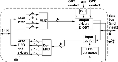
Figure 12.19 also shows another subtle difference between DDR and DDR2 SDRAM devices. The I/O interface of the DDR2 SDRAM device has an additional signal to control the termination characteristic of the input pin. The On-Die Termination (ODT) signal can be controlled by a DDR2 SDRAM memory controller to dynamically adjust the electrical characteristics of the memory system, depending on the configuration of the specific memory system.
12.3.4 Protocol and Architectural Differences
The evolutionary relationship between DDR SDRAM and DDR2 SDRAM device architectures means that the two devices architectures are substantially similar to each other. However, there are subtle architectural and protocol differences that separate the DDR2 SDRAM device from the DDR SDRAM device. For example, DDR2 SDRAM devices can support posted CAS commands, and DDR2 devices now mandate a delay between the column write command and data from the memory controller.
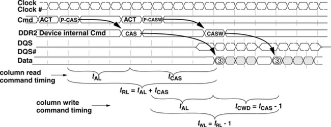
Figure 12.20 illustrates two pipelined transactions to different banks in a DDR2 SDRAM device. The figure shows that the DDR2 SDRAM device is programmable to the extent that it can hold a column access command for a certain number of cycles before it executes the command. The posted CAS command feature allows a DDR2 SDRAM memory controller to treat a row activation command and a column access command as a unitary command pair to be issued in consecutive cycles rather than two separate commands that must be controlled and timed separately. In Figure 12.20, the additional hold time for the CAS command is three cycles, and it is labelled as tAL, for Additional Latency. Figure 12.20 also shows that the DDR2 SDRAM device now requires a write delay that is equivalent to tCAS − 1 number of cycles. With the addition of tAL, column read command timing can be simply referred to as Read Latency, or tRL, and column write command timing can be simply referred to as Write Latency, or tWL.
Differential Strobes and FBGA Packages
In addition to dynamic termination control, DDR2 SDRAM device architecture also contains other features that differentiate it from DDR SDRAM device architecture. For example, DDR2 SDRAM devices can optionally support a differential DQS signal, while DDR SDRAM devices only support a single ended DQS signal. The differential DQS signal enables the DDR2 SDRAM device to bolster the signal integrity of the reference strobe, thus enabling it to operate at higher data rates. In addition to illustrating the progression of the posted column read and posted column write commands, Figure 12.20 also shows that data for column read commands, sent by the DRAM devices, is edge-aligned to the data strobe signal, while data for column write commands, sent by the DRAM controller, is center-aligned to the DQS and DQS# data strobe signals.2
Finally, Figure 12.21 shows a DDR SDRAM device in a TSOP and a DDR2 SDRAM device in a Fine Ball Grid Array (FGBA) package. FBGA packaging is more expensive than TSOP, but the ball grid contacts present less electrical parasitics for the signal transmission line. Consequently, FBGA packaging is required for the higher data rate DDR2 devices, while it remains optional for DDR SDRAM devices.
12.3.5 DDR3 SDRAM
Having learned many lessons in the evolutionary development of DDR and DDR2 SDRAM devices, DRAM device and systems manufacturers have continued on the path of further increasing DRAM device prefetch lengths to enable higher device data rates in the next-generation commodity DRAM device—DDR3 SDRAM. The DDR3 SDRAM device continues the technique of increasing prefetch lengths and employs a prefetch length of 8. Consequently, DDR3 SDRAM devices are expected to attain data rates that range between 800 Mbps per pin to 1.6 Gbps per pin, doubling the range of 400 to 800 Mbps per pin for DDR2 SDRAM devices.3
DDR3 SDRAM devices also contain additional enhancements not found in DDR2 SDRAM devices. For example, DDR3 SDRAM devices of all capacities have at least 8 banks of independent DRAM arrays, while the 8-bank architecture is limited to DDR2 devices with capacities of 1 Gbit or larger. DDR3 SDRAM devices will also have two features that may enable them to reduce refresh power consumption. One optional feature that will enable DDR3 SDRAM devices to reduce refresh power consumption is a temperature-dependent self-refresh mode. In this self-refresh mode, the rate of refresh and current of the self-refresh circuitry will be adjusted automatically by the DDR3 device, depending on the temperature of the device. The second feature that will enable DDR3 devices to reduce refresh power is that a DDR3 device can be programmed to refresh only a subset of the rows that contain data, rather than all of the rows once per fresh loop.4 These features, in combination with the lower 1.5 V supply voltage, enable DDR3 devices to consume less power per unit of storage or unit of bandwidth.
Unfortunately, the high data transfer rate of DDR3 SDRAM devices requires significant trade-off in memory system configuration flexibility, a trade-off that will limit the utility of the device in unbuffered memory systems. To reach the high data rate of DDR3 SDRAM devices, DRAM device and system manufacturers have imposed the limit of two ranks of DRAM devices in a memory system, and the two ranks of DRAM devices are assumed to be located close to each other. Consequently, computer system manufacturers will not be able to design and market computers with traditional, unbuffered memory systems that still allow end-users to flexibly configure the capacity of the memory system as could be done with DDR and DDR2 SDRAM memory systems.
12.3.6 Scaling Trends of Modern-Commodity DRAM Devices
In the decade since the definition of the SDRAM standard, SDRAM devices and their descendants have continued on a general scaling trend of exponentially higher data rates and slowly decreasing timing parameter values for each generation of DRAM devices. Table 12.2 contains a summary of timing parameter values for selected SDRAM, DDR SDRAM, and DDR2 SDRAM devices. Table 12.2 shows that fundamental device operation latencies in terms of wall clock time have gradually decreased with successive generations of DRAM devices, while DRAM device data rates have increased at a much higher rate. Consequently, DRAM device operation latencies have, in general, increased in terms of cycles, despite the fact that the latency values in nanoseconds have decreased in general.
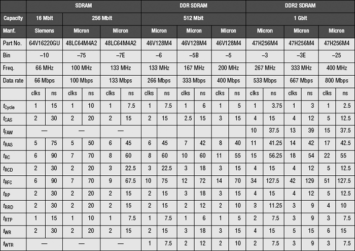
Figure 12.22 shows the scaling trends of commodity DRAM devices from 1998 to 2006. In the time period illustrated in Figure 12.22, random row cycle times in commodity DRAM devices decreased on the order of 7% per year. In contrast, the data rate of commodity DRAM devices doubled every three years. Consequently, the relatively constant row cycle times and rapidly increasing data rates mean that longer requests or a larger number of requests must be kept in flight by the DRAM memory controller to sustain high bandwidth utilization.

Figure 12.22 also shows an anomaly in that the refresh cycle time tRFC has increased rather than decreased in successive generations of DRAM devices, unlike the scaling trends for other timing parameters. Although the tRFC values reported in Table 12.2 are technically correct, the illustrated trend is somewhat misleading. That is, tRFC increased for the DDR2 devices examined over that for the DDR SDRAM devices due to the fact that the DDR SDRAM devices examined in Table 12.2 are 512-Mbit devices, whereas the DDR2 SDRAM devices examined in Table 12.2 are 1-Gbit devices. In this case, the larger capacity means that a larger number of cells must be refreshed, and the 1-Gbit DDR2 DRAM device must take longer to perform a refresh command or draw more current to refresh twice the number of DRAM storage bits in the same amount of time as the 512-Mbit DDR SDRAM device. Table 12.2 shows that DRAM manufacturers have, in general, chosen to increase the refresh cycle time tRFC, rather than significantly increase the current draw needed to perform a refresh command. Consequently, the refresh cycle time tRFC has not decreased in successive generations of DRAM devices when the general trend of increasing capacity in each generation is taken into account.
Table 12.3 contains a summary of modern-commodity SDRAM devices, showing the general trends of lower supply voltages to the devices and higher operating data rates. Table 12.3 also summarizes the effect of the increasing prefetch length in SDRAM, DDR SDRAM, DDR2 SDRAM, and DDR3 SDRAM devices. Table 12.3 shows the worrying trend that the increasing data rate of commodity DRAM devices has been achieved at the expense of increasing granularity of data movement. That is, in a ×4 SDRAM device, the smallest unit of data movement is a single column of 4 bits. With increasing prefetch length, the smallest unit of data movement has also increased proportionally. The increasing granularity of data movement means that the commodity DRAM system is losing randomness of data access, and the higher device bandwidth is achieved only by streaming data from spatially adjacent address locations. The situation is being compounded with the fact that ×8 DRAM devices are far outselling ×4 DRAM devices, and ×4 DRAM devices are only being used in memory systems that require maximum capacity. Consequently, ×4 DRAM devices are now selling at a price premium over ×8 and ×16 DRAM devices.
TABLE 12.3
Quick summary of SDRAM and DDRx SDRAM devices

a400-Mbps DDR SDRAM standard voltage set at 2.6 V.
b16-Mbit density SDRAM devices only have 2 banks in each device.
c256- and 512-Mbit devices have 4 banks; 1-, 2-, and 4-Gbit DDR2 SDRAM devices have 8 banks in each device.
The larger granularity of data movement has serious implications in terms of random access performance as well as memory system reliability. For example, in a DDR2 SDRAM memory system, the loss of a single device will take out 16 bits of data in a ×4 device and 32 bits of data in a x 8 device. Consequently, a minimum data bus width of 144 bits is needed, in combination with sophisticated error correction hardware circuitry to cover for the loss of 16 bits of data in a ×4 device and 32 bits of data in a ×8 device.
12.4 High Bandwidth Path
In 1990, the 80386 processor was the dominant desktop processor, and memory bandwidth was not a limiting issue as it is in more modern memory systems. However, in that same year, Rambus Corp. was founded with a focus to design high-speed chip interfaces, specifically memory system interfaces. Rambus Corp.’s focus on high-speed signaling technology led it to design high bandwidth memory interfaces and systems that differ radically from commodity DRAM memory systems in terms of signaling protocol, system topology, device architecture, and access protocol. As a result of its singular focus on high device and system bandwidth, the high bandwidth path of DRAM device architecture evolution is dominated by memory systems developed by Rambus Corp.
In the years since its founding, Rambus Corp. has had various levels of contribution and involvement in different memory systems. However, two high bandwidth memory systems are often cited when Rambus technology is brought up for discussion: the Direct Rambus Dynamic Random-Access Memory (Direct RDRAM) memory system and the Extreme Data Rate (XDR) memory system. In this section, the unique features of these two memory systems are singled out for examination.
12.4.1 Direct RDRAM
The Direct RDRAM device and system architectures are radically different from the conventional, commodity DRAM device and system architectures. In this section, we begin with the fundamental difference between the Direct RDRAM memory system and the commodity, cost-focused DRAM memory systems by starting with an examination of the high-speed signaling technology developed by Rambus, the Rambus Signaling Level (RSL) signaling protocol. RSL enabled Rambus Corp. to design high-speed DRAM device interfaces. However, the relatively slow DRAM circuits designed for use in low-cost commodity DRAM devices mean that the high-speed RSL signaling protocol must be coupled with suitable device and system architectures to attain high values of practical, sustainable bandwidth. In the following sections, the signaling technology, system architecture, device architecture, and access protocol of the Direct RDRAM memory system are systematically examined. The systematic examination of the Direct RDRAM memory system architecture begins with an examination of RSL.
The Rambus Signaling Level (RSL)
The RSL was Rambus’ first signaling technology. RSL was designed as a high-speed, singled-ended, multidrop, bidirectional bus signaling technology. RSL is designed as a signaling technology that can support a variable number of loads on the same bus—between 1 and 32 DRAM devices can be connected to the same bus. RSL debuted with data rates of 500 Mbps and reached over 1.2 Gbps in various configurations.
Figure 12.23 shows that the RSL is defined to swing between 1.0 and 1.8 V. RSL is designed to operate as a high-speed signaling system that makes use of current mode output drivers with carefully controlled slew rates to deliver low-voltage signals across transmissions lines with carefully controlled impedance characteristics.
Memory System Architecture
The system architecture of the Direct RDRAM memory system differs dramatically from system architectures of SDRAM and DDRx SDRAM memory systems. The key elements of the Direct RDRAM memory system architecture that differentiate it from SDRAM and DDRx SDRAM memory system architectures are path-matched address, command and data bus topology, separate row and column address channels with encoded command packets, separate data channel, multiple cycle, packet-based command and address assertion from memory controller to memory device, and the absence of a critical word forwarding data burst.
The system architecture of the Direct RDRAM memory system was designed to sustain high pin-bandwidth regardless of the number of DRAM devices in the memory system. The motivation for this design decision is that it allows for a high degree of performance scalability with multiple channels of memory, regardless of the number of DRAM devices per channel. In theory, an embedded system with a single channel memory system with a single DRAM device in the memory system can enjoy as much pin-bandwidth as a server system with multiple channels of memory and fully populated with 32 devices per channel. Unlike high data rate DDR2 and DDR3 memory systems that rely on multiple ranks of DRAM devices to collectively provide sufficient bandwidth to saturate the channel, a single-rank Direct RDRAM memory system can provide as much bandwidth as a multi-rank Direct RDRAM memory system.
Device Architecture
Figure 12.24 illustrates the device organization of a 288-Mbit Direct RDRAM device with 32 interleaved and dependent (32d) banks internally. The Direct RDRAM device can be architected to contain different numbers of banks. The organization illustrated in Figure 12.24 contains 32 dependent banks.5 In the 32d Direct RDRAM device architecture, each bank is split into two halves, an upper half bank and a lower half bank, and adjacent banks share common sets of sense amplifiers. That is, the lower half of bank i shares the same set of sense amplifiers with the upper half of bank i + 1. Consequently, adjacent banks i and i + 1 cannot both be open at the same time.
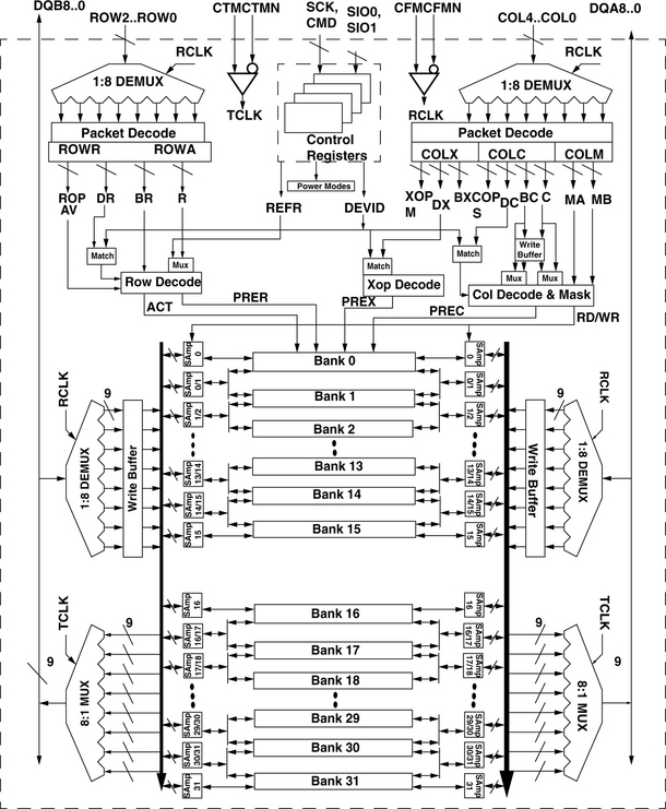
One difference between Direct RDRAM memory systems versus SDRAM and DDRx SDRAM memory systems is that SDRAM and DDRx SDRAM memory systems rely on wide data busses with a non-power-of-two number of devices in parallel to provide the requisite number of data and check bits for error detection and correction. In contrast, a single Direct RDRAM device may form the entire data bus width of a Direct RDRAM memory system. Consequently, different versions of Direct RDRAM devices are used in different Direct RDRAM memory systems. Direct RDRAM memory systems that do not require error correction use Direct RDRAM devices with a 16-bit-wide data bus, and Direct RDRAM memory systems that require error correction use Direct RDRAM devices with an 18-bit-wide data bus. Figure 12.24 illustrates a Direct RDRAM device with an 18-bit-wide data bus. The figure shows that the 18-bit-wide data bus is organized as two separate 9-bit-wide data busses.
Unlike SDRAM and DDRx SDRAM devices where a given command and the associated address are sent in a single clock cycle, Direct RDRAM devices encode the command and address into a multi-cycle packet that must be buffered, de-multiplexed, and decoded by the Direct RDRAM device. In the case of a column read command, a read command packet (40 bits in size) is sent over the 5-bit-wide COL[4:0] column command bus on both the rising edge and the falling edge of the clock-from-master (CFM) clock signal. The 40-bit-wide packet is received and decoded by the Direct RDRAM device into COLX, COLC, and COLM command and address fields. The Direct RDRAM device then moves the requested data from the array of sense amplifiers through the 8:1 multiplexor onto the data bus. In this manner, the data prefetch architecture of Direct RDRAM devices is very similar to the internal device architecture of DDR3 SDRAM devices. However, unlike DDR3 SDRAM devices, Direct RDRAM devices do not support burst reordering to send the critical word first.
Topology
To take advantage of the high-speed signaling system, Rambus designed a new system topology for Direct RDRAM. Figure 12.25 shows that each Direct RDRAM device appears on a Direct DRAM channel as a single load. Figure 12.25 presents a topological view of the Direct RDRAM memory system with the memory controller connected to two memory modules, and each module contains four memory devices. The memory module for the Direct RDRAM memory system is referred to as a Rambus In-line Memory Module (RIMM) by Rambus. Each memory device illustrated in the Direct RDRAM memory system in Figure 12.25 presents a 16-bit-wide data interface to the data bus. In Figure 12.25, all of the Direct RDRAM devices are connected on the same channel with a 16-bit-wide data bus. In essence, each Direct RDRAM device is a single rank of memory in a Direct RDRAM memory system.
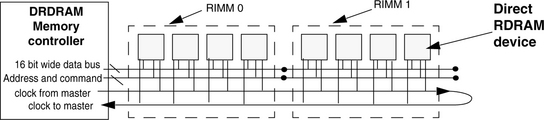
In a Direct RDRAM memory system, the clock-from-master signal, the clock-to-master signal, the column address and command bus, the row address and command bus, and the two 8-bit-wide data busses are routed in parallel. Unlike the mesh topology of the SDRAM and the DDRx SDRAM memory systems, the topology of the Direct RDRAM memory system allows all of the signal interfaces of the DRAM device to operate with minimal skew relative to the system clock signals. The Direct RDRAM memory system uses a scheme where the clock signals propagate alongside data signals to minimize timing skew between clock and data. The minimal clock-data timing skew means that the Direct RDRAM memory system can avoid the insertion of idles in the protocol to account for timing uncertainties and achieve high bandwidth efficiency. The arrangement of the memory device in the Direct RDRAM memory system also means that with more devices, the bus turnaround time increases and results in longer memory latency.
Access Protocol
The memory-access protocol of the Direct RDRAM memory system is quite different from access protocols of traditional memory systems such as SDRAM, DDR SDRAM, and DDR2 SDRAM memory systems. As a consequence of the matched topology of the clock, data, and command and address busses, the Direct RDRAM memory controller encodes all commands and addresses into packets6 and transmits them in 8 half cycles,7 a period of time called an octcycle, from the controller to the DRAM device. In the case of row commands, the Direct RDRAM controller encodes the row address and access commands into row access command packets that are 24 bits in length and transports the 24-bit-long packets from the controller to a Direct RDRAM device over 3 signal wires in 8 half cycles. In the case of column access commands, the Direct RDRAM controller encodes the column addresses and column access commands into packets that are 40 bits in length for transport to a Direct RDRAM device over 5 signal wires in 8 half cycles.
The Direct RDRAM memory system transports data in a manner that is similar to the command transport mechanism. In the case of a column read command, 128 bits of data are transported from a single Direct RDRAM device over 16 signal wires in 8 half cycles to the memory controller. The timing of a memory read command in a Direct RDRAM memory system is illustrated in three separate steps in Figure 12.26. The figure shows that the Direct RDRAM memory controller first packs and encodes a row activation command and then transmits the packed row activation command over the span of four clock cycles in step 1. The packed column access command is then transmitted to the Direct RDRAM device in step 2. Finally, in step 3, data is returned to the controller by a given Direct RDRAM device (device 0 in Figure 12.26) in over 8 half cycles. The 128 bits, or 16 bytes, of data are also referred to as a dualoct by Rambus.
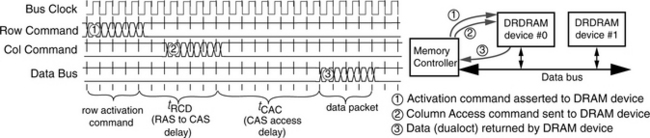
One interesting detail about the Direct RDRAM memory-access protocol illustrated in Figure 12.26 is that the Direct RDRAM controller began to transmit the column read command almost immediately after the row access command, before tRCD timing had been satisfied. The reason that the transmission of the column read command can begin almost immediately after the transmission of the row access command is that each command packet must be buffered, decoded, and then executed by the addressed Direct RDRAM device. Consequently, the column access command shown as step 2 in Figure 12.26 is not decoded until the transmission of the command has been completed and the entire packet has been received by the Direct RDRAM device. The optimal timing to minimize delay is then to coincide the row-activation-to-column-access delay with the end of the column access packet as shown in Figure 12.26.
The Direct RDRAM memory system is designed to sustain high bandwidth throughput, and the Direct RDRAM memory-access protocol allows a large combination of different memory-access commands to be issued by the memory controller consecutively without the need for idle cycles. Figure 12.27 illustrates the full utilization of the data bus by showing three consecutive column read commands that return data to the memory controller without the presence of any idle cycles between data packets on the data bus. Figure 12.27 shows two consecutive column read commands to device #0, followed by a third command sent to device #1. The figure then shows the return of data by the memory devices after the appropriate CAS delay. In theory, no idle cycles are needed in between column read commands, since the data transmission on the data bus is synchronized by the common clock-to-master signal, even in the case where the column read commands are sent to different Direct RDRAM devices in the Direct RDRAM channel.8

The Write-to-Read Turnaround Issue
Figure 12.28 illustrates the problematic case of a column read command that follows a column write command in commodity DRAM devices such as a DDR SDRAM device. The figure illustrates that despite the existence of separate read and write FIF buffers and drivers, both read data and write data must share the use of internal and external data busses through the I/O gating structure. The sharing of the data busses means that write data must be driven into and through the internal data busses to the selected bank of sense amplifiers before data for a subsequent read command to the same device can be placed onto the internal data bus. The bottleneck of the internal data bus leads directly to long write-to-read turnaround times in high data rate DRAM devices.
Write Buffer in Direct RDRAM Devices
To reduce the long write-read turnaround time in high data rate DRAM devices, Rambus designed Direct RDRAM devices and XDR DRAM devices with specialized structures to alleviate the write-to-read turnaround problem. The solution to the write-to-read turnaround problem implemented in the Direct RDRAM device is through the use of a write buffer. The existence of the write buffer in the Direct RDRAM device means that as soon as data is written into the write buffers, the I/O gating resource can be used by a subsequent column read command. Figure 12.29 illustrates the sequence of three column access commands to a Direct RDRAM device: a column write command followed by a column read command that is, in turn, followed by a retire command. Figure 12.29 illustrates that the write-to-read turnaround time is significantly reduced through the use of the write buffer. Essentially, actions typically performed by column write commands are separated into a write-into-write-buffer command and a retire-from-write-buffer-into-sense-amplifier command. The separation of the column write command enables a subsequent read command to be issued immediately after a column write command since the column write command does not have to immediately drive the data through the internal datapath and into the sense amplifiers.
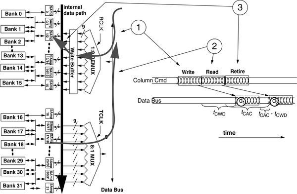
The use of the write buffer by the Direct RDRAM device has several implications from the perspective of the memory-access protocol. First, a column write command places write data temporarily in the write buffer, but addresses of subsequent column read commands are not checked against addresses of pending data in the write buffer by the Direct RDRAM device. The interesting result is that a column read command that immediately follows a column write command to the exact same location in a Direct RDRAM device will read stale data from the sense amplifiers while the most recent data is held in the write buffers. The use of the write buffer by the Direct RDRAM device thus requires the memory controller to keep track of the addresses of column write commands that have not yet been retired from the write buffer to enforce memory consistency.
The use of write buffers to alleviate the write-to-read turnaround time directly increases the complexity of the DRAM device as well as the complexity of the DRAM memory controller. In the case of the DRAM device, die area devoted to the write buffer increases the die cost of the DRAM device. From the perspective of the memory-access protocol, the memory controller has to manage a new retire-write-data command, further increasing its complexity.
12.4.2 Technical and Pseudo-Technical Issues of Direct RDRAM
In the late 1990s, the Direct RDRAM memory system was chosen by Intel Corp. as the next-generation memory system that would replace the 100-MHz SDRAM memory system. However, due to a number of issues, Direct RDRAM memory systems failed to gain market acceptance and did not replace SDRAM as the mainstream memory system. Instead, a more moderate evolutionary path of DDRx SDRAM memory systems replaced the SDRAM memory system. The issues that prevented Direct RDRAM memory systems from gaining market acceptance consisted of a number of technical issues that were primarily engineering trade-offs and a number of non-technical issues that were related to the licensing of the Direct RDRAM memory system by Rambus Corp. to DRAM device manufacturers and system design houses. In this chapter, the focus is placed on the technical issues rather than the business decisions that impacted the failure of the Direct RDRAM memory system to achieve commodity status. Moreover, the challenges faced by Direct RDRAM memory systems in attempting a revolutionary break from the commodity SDRAM memory system are quite interesting from the perspective that future memory systems that attempt similar revolutionary breaks will have to overcome similar challenges faced by the Direct RDRAM memory system. Consequently, the engineering trade-offs that increased the cost of implementation or reduced the performance advantage of the Direct RDRAM memory systems are examined in detail.
Die Size Overhead
In practical terms, the Direct RDRAM memory system increased memory device complexity to obtain higher pin-bandwidth and increased data transport efficiency. For example, the baseline Direct RDRAM device contained 16 or 32 dependent banks, requiring separate bank control circuitry and arrays of sense amplifiers. Each Direct DRAM device also contained circuitry to carefully manage the electrical characteristics of the Direct RDRAM device. The high-speed RSL signaling interface further required separate I/O voltage rings for the Direct RDRAM device. Collectively, the sophisticated architectural features and electrical control circuitry added significantly to the die cost. Consequently, Direct RDRAM devices were approximately 20∼30% larger than SDRAM devices at the 64-Mbit node. This die size overhead resulted from a combination of the required circuit overhead and the fact that these first-generation devices were designed for speed rather than die size. Fortunately, the circuit overhead of Direct RDRAM devices was relatively constant in terms of the number of transistors. Consequently, the die size overhead of Direct RDRAM devices, as a percentage of die area, decreases with increasing DRAM device capacity. At the 128-Mbit density node, Toshiba produced an SDRAM device with a die size of 91.7 mm2, while its Direct RDRAM device on the same process had a die size of 103 mm2, making the die size overhead 12% for Toshiba at the 128-Mbit node. The die size overhead for Direct RDRAM devices was expected to drop below 10% for the 256-Mbit density node and decrease further at higher density nodes.
Sophisticated System Engineering Requirement
The high system-level signaling rates of the Direct RDRAM memory system required careful control and understanding of the electrical characteristics of the memory controller I/O interface, the system board, the memory modules, and the DRAM device package and I/O interface. Analogously, the issues in implementing Direct RDRAM memory systems were similar to the issues that necessitated the PC100 standard, and the solutions were similar: significant amounts of engineering resources had to be devoted to design a high data rate memory system. Consequently, system manufacturers were reluctant to devote the engineering resources required to implement Direct RDRAM memory systems. In particular, some low-cost-focused system manufacturers lacked the engineering resources required to design low-cost Direct RDRAM memory systems.
One issue that illustrated the importance of engineering resources in the deployment of cost-effective Direct RDRAM memory systems is the issue of multilayer system boards. The Direct RDRAM memory system architecture required matching signal flight times for parallel signals on various command and data busses. To minimize crosstalk and ensure signal integrity, first-generation proof-of-concept system boards that implemented Direct RDRAM memory systems were designed on 8-layer PCBs, and many second-generation system boards that shipped commercially with Direct RDRAM memory systems were designed on 6-layer PCBs. Compared to commodity systems that used 4-layer PCBs, the 6-layer system board further increased cost to the early implementation of Direct RDRAM memory systems. Finally, with the passage of time and the devotion of engineering resources by Rambus and various system manufacturers, the system-level cost issue of Direct RDRAM memory systems was eventually brought to parity with commodity systems as Direct RDRAM memory systems on 4-layer PCBs were proven to be practical.
Advanced Packaging and Testing Equipment Requirement
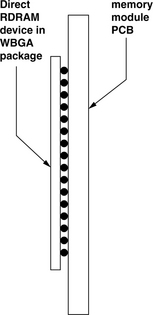
The high signaling rate Direct RDRAM device required careful control of the electrical characteristics of the DRAM device package and I/O interface. Consequently, Direct RDRAM devices could not use similar low-cost TSOPs and SOJ packages that were used for SDRAM devices. Instead, Direct RDRAM devices were shipped with BGA packages that minimized the impedance contributions of the pin interface of the package. Figure 12.30 illustrates one type of BGA packaging used for Direct RDRAM devices. Unfortunately, the use of the BGA package further added cost to DRAM device and memory module manufacturers that were not accustomed to the new packaging. For example, memory module manufacturers could not visually inspect the solder connections between the BGA package and the memory module as they could with SOJ and TSOPs. Consequently, new equipment had to be purchased to handle the new packaging, further increasing the cost delta between Direct RDRAM memory systems and the then-commodity SDRAM and DDR SDRAM memory systems.
Heat Density—Heat Spreader—Enforced Idle Cycles
In the classical mesh topology of SDRAM and DDRx SDRAM memory systems, multiple DRAM devices are connected in parallel to form a given rank of memory. Moreover, high data rate DDR2 and DDR3 SDRAM devices do not contain enough banks in parallel in a single rank configuration to fully saturate the memory channel. Consequently, the on-chip and in-system data movements associated with any given command issued by the memory controller are always distributed across multiple DRAM devices in a single rank and also typically across different ranks in standard 64- or 72-bit-wide SDRAM and DDRx SDRAM memory systems. In contrast, the Direct RDRAM memory system is architected for high bandwidth throughput, and a single Direct RDRAM device provides full bandwidth for a given channel of Direct RDRAM devices. However, the ability of the single Direct RDAM device to provide full bandwidth to the memory channel means that the on-chip and in-system data movements associated with a given command issued by the memory controller are always limited to a single DRAM device. Moreover, Figure 12.31 illustrates that in the worst-case memory-access pattern, a sustainable stream of row activation and column access commands can be pipelined to a single device in a given channel of the Direct RDRAM memory system. Consequently, localized hot spots associated with high access rates to a given device can appear and disappear on different sections of the Direct RDRAM channel. The localized hot spots can, in turn, change the electrical characteristics of the transmission lines that Direct RDRAM memory systems rely on to deliver command and data packets, thus threatening the functional correctness of the memory system itself. To counter the problem of localized hot spots in Direct RDRAM memory systems, Rambus Corp. deployed two solutions: heat spreaders and new command issue rules designed to limit access rates to a given Direct RDRAM device. Unfortunately, the use of heat spreaders on the RIMMs further increased the cost of the Direct RDRAM memory system, and the new command issue rules further increased controller complexity and decreased available memory bandwidth in the Direct RDRAM memory system.
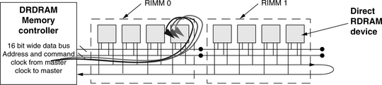
Low Request Rate Systems
The Direct RDRAM memory system provided a revolutionary approach to memory system architecture that required significant cost adders in many different components of the memory system. Consequently, first-generation Direct RDRAM memory systems were significantly more expensive than SDRAM memory systems. However, these first-generation Direct RDRAM memory systems were used in Pentium III-based computer systems, and these Direct RDRAM memory systems did not illustrate significant performance benefits over SDRAM-based memory systems to justify their cost premium.
Figure 12.32 shows that in the memory-access sequence of a Direct RDRAM memory system, the controller first sends a packet command to the Direct RDRAM device, and then the DRAM device buffers the command, decodes it, moves the data to the I/O interface, and then bursts that data over 8 half cycles back to the controller. Memory access in the Direct RDRAM memory system thus suffers from the additional latency components of command transmission to the DRAM device and data burst time back to the controller. Consequently, the SDRAM memory system has lower idle system latency as compared to the Direct RDRAM memory system. Figure 12.32 illustrates that the advantage of the Direct RDRAM memory system is that its higher bandwidth and higher efficiency allows it to return data with lower average latency when it is coupled with a processor that has a high rate of memory access. Unfortunately, first-generation Direct RDRAM memory systems were primarily coupled to uniprocessor Pentium III-based systems that did not and could not sustain a high rate of memory access. Potentially, Direct RDRAM memory systems coupled to advanced high-frequency, multi-threaded, and multi-core processors would have provided the tangible performance benefit that could justify the cost premium. Unfortunately, the average consumer could not envision the advanced processors that were yet to come, but could readily observe that the Direct RDRAM memory system did not present significant performance advantage over SDRAM memory systems when attached to Pentium III-based systems.
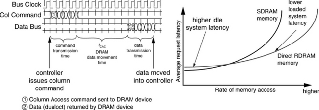
Different Devices for Different Systems
In a Direct RDRAM memory system, a single Direct RDRAM device returns a dualoct for a given column access command. However, memory systems designed for reliability require additional data storage locations to store check bits. In traditional commodity memory systems, the check bits are stored in additional DRAM devices as the width of the data bus is increased from 64 to 72 bits. Consequently, the same DRAM devices can be used in desktop computers that do not require error correction and in high-end servers that do. In contrast, the 16-bit data bus width of the Direct RDRAM memory system means that it was not practical to create an analogous memory system where a single logical channel of memory consists of 9 physical channels of Direct RDRAM devices in parallel. Aside from the extraordinary cost of 9 physical channels of Direct RDRAM memory, a single column access command to such a memory system would move 144 bytes of data, a granularity that is too large for the cacheline sizes of all mainstream processors.9 Consequently, different versions of Direct RDRAM devices had to be designed for error correcting memory systems and systems that did not require error correction. At the 64-Mbit density node, 64-Mbit Direct RDRAM devices with 16-bit-wide data busses were available alongside 72-Mbit Direct RDRAM devices with 18-bit-wide data busses. Similarly, 144-, 288-, and 576-Mbit Direct RDRAM devices were available alongside 128-, 256-, and 512-Mbit devices in each density node, respectively. The different versions of Direct RDRAM devices split the volume demand for Direct RDRAM devices, providing yet another obstacle that hindered cost-reduction efforts in Direct RDRAM memory systems.
Lessons for Future Memory Systems
The Direct RDRAM memory system introduced a high level of complexity and new cost adders into the memory system, but the fact that it was coupled to a relatively low-frequency Pentium III-based system meant that it did not demonstrate its best-case performance advantage over lower cost SDRAM and DDR SDRAM memory systems. Consequently, it met a great deal of resistance and encountered numerous obstacles in its way of reaching high volume production status, approaching price parity with SDRAM memory systems and demonstrating a tangible performance advantage in production systems. Ultimately, the Direct RDRAM memory system failed to reach commodity status. However, the technical challenges faced by Direct RDRAM memory systems were important lessons that Rambus Corp. heeded in the design of its next-generation high bandwidth memory system, the XDR memory system.
12.4.3 XDR Memory System
Rambus Corp., having learned valuable lessons from the drawbacks of the Direct RDRAM memory system, proceeded to design its next-generation high bandwidth memory system that avoided many of the technical pitfalls that hindered acceptance of the Direct RDRAM memory system. The Extreme Data Rate (XDR) memory system has been designed to further increase DRAM device and memory system signaling rate, yet at the same time to reduce system design complexity and DRAM device overhead.
Topology
Figure 12.33 illustrates the basic system topology of the XDR memory system. The figure shows that in the XDR memory system, as in DDRx SDRAM systems, the command-and-address busses operates at a relatively lower data rate as compared to the data bus. In the XDR memory system, the command and address datapath is a path-length-matched, unidirectional datapath that the XDR memory controller uses to broadcast command and address information to DRAM devices. Figure 12.33 also shows that the XDR controller uses FlexPhase to do skew compensation on the datapath—removes skew on read data coming into the controller and adds skew to ensure that write data reaches DRAM device interface in sync.
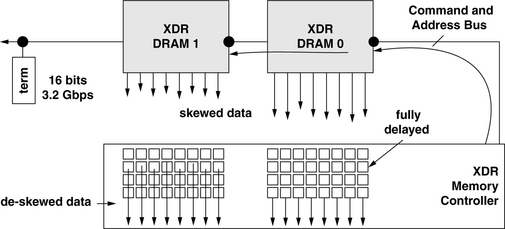
Device Architecture
Figure 12.34 illustrates the device organization of an XDR device. The XDR DRAM device is characterized by numerous features that distinguish it from the Direct RDRAM device. For example, the XDR DRAM device has a prefetch length of 16, so the minimum burst length is 16. However, the XDR device architecture has been designed with variable device data bus width control so that a device may be configured with a data bus width as low as 1 bit. Consequently, the minimum granularity of data movement in such a device may be as small as 16 bits. Figure 12.34 also shows that the XDR device is internally organized into two different, odd and even, bank sets.
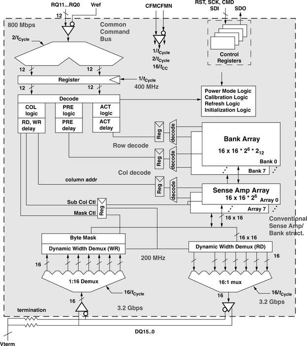
Finally, Figure 12.34 shows that the XDR device differs from the Direct RDRAM device in that unlike the Direct RDRAM device, the XDR DRAM device has a common command bus that is used by row access commands as well as column access commands. Moreover, unlike the Direct RDRAM device, the XDR DRAM device does not have a write buffer. Instead, it relies on the differing bank sets and an intelligent controller to alleviate the write-to-read data bus turnaround issue.
Signaling
Figure 12.35 shows the octal data rate signaling system that Rambus Corp. introduced with the XDR memory system. In this signaling system, a relatively slow master clock signal (400∼800 MHz) is shared by both the memory controller and the DRAM device. The DRAM device and the memory controller use current mirrors to transmit differential signals that are locked in-phase with the system clock signal, but operate at four times the frequency of the system clock signal. Data is transmitted on both edges of the signal, so 8 1-bit symbols per pin pair are transmitted in every clock cycle. The low voltage swing, point-to-point, differential signaling enables high bandwidth in commodity ASIC and DRAM processor technologies at the cost of higher power consumption.

FlexPhase
In the XDR memory system, Rambus Corp. uses a system of bit-adjustable DLL circuitry to remove bit-to-bit signal skew from the high-speed parallel data bus. This system of bit-adjustable DLL circuitry is referred to as FlexPhase. Figure 12.35 shows how Rambus uses the FlexPhase circuit to account for differences in signal flight time. FlexPhase takes care of data-to-data skew, and it can be recalibrated to lock in new phase differentials to account for thermal drifts between cold and warm systems. Figure 12.35 shows that the FlexPhase circuitry is placed in the controller interface. In this manner, the FlexPhase technology removes the path-length matching requirement from the XDR memory system without increasing the cost of the DRAM device. In this case, the additional cost is paid for in terms of increased controller sophistication.
XDR Early Read After Write
To counter the various drawbacks of a write buffer in Direct RDRAM devices, Rambus did not include write buffers in the design of its next-generation, high-performance XDR DRAM device. Instead, XDR DRAM devices are architected to support a feature that Rambus refers to as the Early Read After Write (ERAW) feature. Essentially, XDR devices avoid the large write-to-read command overhead by using separate internal paths for banks separated into odd and even sets. In this organization, a read command can proceed in parallel with a write command, as long as the read and write commands are directed to banks in different bank sets. Figure 12.36 shows that although the write-to-read turnaround overhead still occupies several cycles, the overhead is much smaller than if the write and read commands are issued to the same set of banks.
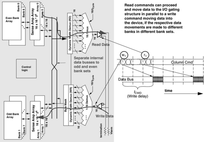
12.5 Low Latency
The proliferation of low-cost commodity DRAM devices means that high-speed, low-latency SRAM devices have been pushed into increasingly small niches as design engineers seek to use DRAM devices wherever they can to reduce system cost. However, even as DRAM devices replace SRAM in more and more applications, the desire for lower-than-commodity-DRAM latency characteristics remains. Consequently, DRAM device manufacturers have been developing specialty low-latency DRAM devices as semi-commodity, moderately low-latency replacements for SRAM replacement application. Two families of DRAM devices, the Reduced Latency DRAM (RLDRAM) and Fast Cycle DRAM (FCRAM), have been designed specifically to target the low-latency SRAM replacement market.
12.5.1 Reduced Latency DRAM (RLDRAM)
RLDRAM is a low-latency DRAM device with random access latency as low as 10–12 ns and row cycle times as low as 20 ns. The first-generation RLDRAM device was designed by Infineon to meet the demands of the market for networking equipment. Subsequently, Micron was brought in as a partner to co-develop RLDRAM and provide a second source. However, Infineon has since abandoned RLDRAM development, and Micron proceeded ahead to develop the second-generation RLDRAM II. RLDRAM and RLDRAM II were designed for use in embedded applications. Primarily, RLDRAM is designed for the network market. However, it may also be used for other applications where cost is less of a concern, low latency is a highly desirable feature, and smaller-than-commodity-DRAM capacity is not an issue. For example, RLDRAM may be used as a large lookup table or a large off-chip cache. RLDRAM has been designed with an SRAM-like mentality in that it is designed for SRAM-like random access to any part of the DRAM device; row address and column addresses are combined together and sent as a single access command.
12.5.2 Fast Cycle DRAM (FCRAM)
In contrast to RLDRAM, Fujitsu and Toshiba’s FCRAM achieves low-latency data access by segmenting the data array into multiple subarrays, only one of which is driven during a row-activation command. The sub-row activation process effectively decreases the size of an array and improves access time. Unlike RLDRAM, FCRAM was designed with a DDRx SDRAM-like mentality, where row access commands and column access commands are sent separately, and the FCRAM command set was designed specifically to mimic the DDRx SDRAM command set. The purpose of the commonality is to enable controller designs that can use either FCRAM or commodity DDRx SDRAM devices. Finally, differing from RLDRAM devices, FCRAM was designed with a DIMM specification.
12.6 Interesting Alternatives
12.6.1 Virtual Channel Memory (VCDRAM)
Virtual channel adds a substantial SRAM cache to the DRAM that is used to buffer large blocks of data (called segments) that might be needed in the future. The SRAM segment cache is managed explicitly by the memory controller. The design adds a new step in the DRAM-access protocol: a row activate operation moves a page of data into the sense amplifiers; “prefetch” and “restore” operations (data-read and data-write, respectively) move data between the sense amps and the SRAM segment cache one segment at a time; and column read or write operations move a column of data between the segment cache and the output buffers. The extra step adds latency to read and write operations, unless all of the data required by the application fits in the SRAM segment cache.
12.6.2 Enhanced SDRAM (ESDRAM)
Like EDO DRAM, ESDRAM adds an SRAM latch to the DRAM core, but whereas EDO added the latch after the column multiplexor, ESDRAM adds it before the column multiplexor. Therefore, the latch is as wide as a DRAM page. Though expensive, the scheme allows for better overlap of activity. For instance, it allows row precharge to begin immediately without having to close out the row (it is still active in the SRAM latch). In addition, the scheme allows a write-around mechanism whereby an incoming write can proceed without the need to close out the currently active row. Such a feature is useful for write-back caches, where the data being written at any given time is not likely to be in the same row as data that is currently being read from the DRAM. Therefore, handling such a write delays future reads to the same row. In ESDRAM, future reads to the same row are not delayed.
1Memory system block diagram taken from 1103 data sheet.
2Read data in SDRAM devices is edge-aligned to the clock signal, while write data is center-aligned to the clock signal. The data timing described herein for DDR2 is similar for DDR, DDR2, and DDR3 SDRAM devices.
3At the time of the writing of this text, discussions are underway to extend the range of DDR3 data rate past 2 Gbps.
4Partial array refresh is also present in DDR2 SDRAM devices.
5A 4 independent (4i) banks per device architecture was promoted as a cost reduction initiative for desktop systems that are typically configured with multiple DRAM systems on a given RIMM. However the initiative did not gain traction, and the 32d device architecture was the primary device architecture at the 256-/288-Mbit device node.
6The command and address packets are not network packets with a header and payload. Rather, these packets are simply multi-cycle, fixed-duration, predefined format, command and address data sent by the controller to the DRAM device.
7The Direct RDRAM memory system sends and receives data, commands, and addresses on each edge of a clock signal. Consequently, in the Direct RDRAM memory system, the time period of 8 half cycles is equal to 4 full clock cycles.
8In theory, although no idle cycles are needed in between any two column read commands to open pages in a Direct RDRAM memory system, idle cycles are sometimes inserted into Direct RDRAM memory systems between column access commands to reduce the activity rate of the Direct RDRAM device and to reduce the peak power dissipation of Direct RDRAM memory systems and Direct RDRAM devices.
9Intel’s Itanium and IBM’s server-oriented POWER processors do have 128-byte cachelines, but neither system seriously contemplated such a memory system.