
Cache Case Studies
This chapter presents details of cache organizations from three different contemporary microprocessors, mainly the Motorola MPC7450 (PowerPC ISA), the AMD Opteron (x86-64 ISA), and the Intel Itanium-2 (EPIC ISA) designs.
The logical organization of each cache architecture, including every level of the cache hierarchy, is first presented in brief detail (since these concepts have been explained thoroughly in the preceeding chapters), while notable features that are interesting in specific implementations are given more detailed explanations. This is followed by a presentation of the microprocessor block diagram, where each cache resides, to show how each cache interfaces to their respective processor pipeline. In addition, some in-depth circuit details will be shown to communicate important concepts (mainly from the Intel Itanium-2 with the help of published details regarding the internal circuitry). Finally, techniques used by each cache to maintain cache coherency are presented.
6.1 Logical Organization
The Motorola MPC7450 microprocessor supports three level of caches. The first two levels of the cache are implemented on-chip, while the data array for the third-level cache is designed to be implemented off-chip (the tags and status bits are implemented on-chip to enable fast miss detection to partly hide the slow off-chip access to the main data array).
The logical organization of the three cache levels showing their size, associativity, and other relevant information is shown in Table 6.1.
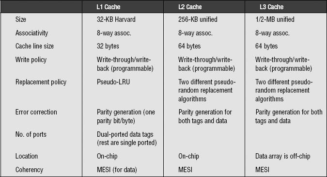
Some of the interesting features of the MPC7450 caches:
• The caches can either be disabled (i.e., no caches at all) or locked using software control. In this way, access times to data can be made predictable, which gives the system a better chance of performing well in a real-time environment.
• Each individual level of the cache can be configured to utilize either write-through or write-back write policies. The granularity of this configuration is chosen to be either a single page or a single cache block (with a cache block being, in PowerPC terminology, the smallest size defined by its own coherency status bits). In this way, programmers are given the flexibility to fine-tune the write policy depending on the application.
• The caches are well designed to provide 128-bit data to and from the load/store unit, which interfaces directly with the processor’s vector units and register files. This allows it to efficiently support the strong SIMD capability of the PowerPC and its Altivec vector instructions.
6.1.2 AMD Opteron
The single-core, 64-bit AMD Opteron processor supports two levels of caches, both of which are implemented completely on-chip. The logical organization of the two caches is listed in Table 6.2.
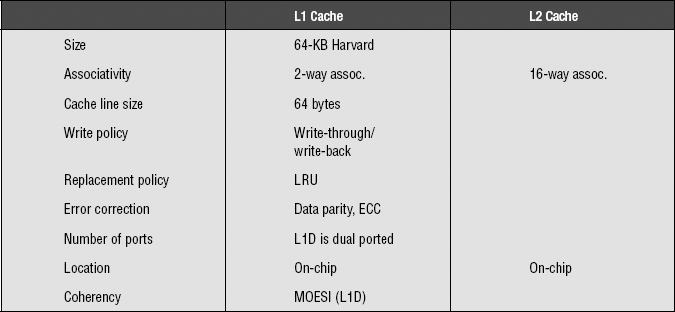
An interesting feature of the Opteron cache:
• The Opteron L2 cache is an exclusive cache; it only contains victim or copy-back cache blocks (that are to be written back to the memory subsystem) as a result of conflict misses. By using this exclusive cache architecture, the effective size of the entire cache system is increased compared to an inclusive cache approach.
6.1.3 Intel Itanium-2
The Intel Itanium-2 microprocessor, like the MPC7450, has three levels of cache. Unlike the MPC7450, though, all three levels of this cache are implemented completely on-chip. The logical organization and other relevant information for the three cache levels are shown in Table 6.3.
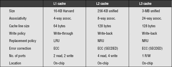
The Intel Itanium-2 cache hierarchy has a number of important features and optimizations:
• All three cache levels employ single-ended sensing as opposed to double-ended or differential sensing during bitline reads. Although differential sensing has been traditionally considered to be more tractable and easier to work with whenever working with low-swing voltage nodes is necessary, the designers believed that single-ended sensing scales well with technology and that it is much easier to treat the bitlines as full-swing logic instead of low swing.
• The L1 cache is optimized for latency and to keep up with the fast core clock. The L2 cache is optimized for bandwidth, as can be seen by the large number of read and write ports that are available to the L1 cache for fills so that access reordering can easily be accomplished. The L3 cache is optimized for area efficiency, as is evident by its huge size and the presence of only a single port. By ensuring a large L3 cache size, the amount of off-chip accesses caused by cache misses should be significantly reduced.
6.2 Pipeline Interface
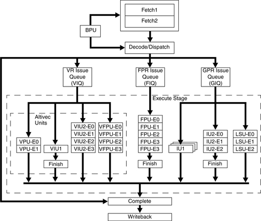
The entire block diagram of the Motorola MPC7450 microprocessor is shown in Figure 6.1. The figure shows the connection of the L1 caches (in the upper right corner of the diagram) to the fetch unit, the load/store unit, and the lower levels of the memory hierarchy (bottom part of the diagram).
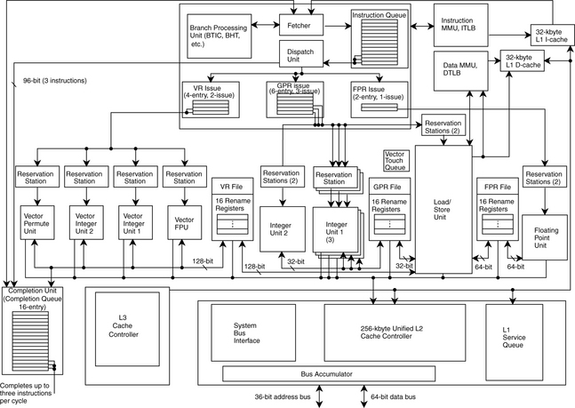
Figure 6.2 shows how these logical blocks fit within the actual framework of the processor pipeline. The L1 instruction cache is accessed sometime during the fetch stages, while the L1 data cache is accessed in the load/store unit stages.
6.2.2 AMD Opteron
The block diagram of the AMD64 microprocessor is shown in Figure 6.3. Within the processor itself, the L1 instruction cache interfaces to the instruction-fetch (IF) unit, and the L1 data cache interfaces to the processor load/store unit. The load/store unit and data cache interface are shown in Figure 6.4.


6.2.3 Intel Itanium-2
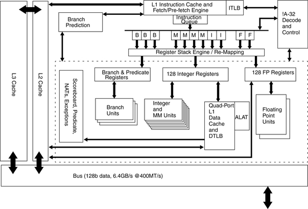
A block diagram of the entire Intel Itanium-2 microprocessor is shown in Figure 6.5, showing the locations of the caches relative to the other units in the core. One of the most interesting things that can be seen in the diagram is the connection of the floating point unit directly to the L2 cache instead of the L1 cache.
6.3 Case Studies of Detailed Itanium-2 Circuits
In this section, we explore some of the interesting circuit techniques and topologies that were used in the design of the Itanium-2 caches.
6.3.1 L1 Cache RAM Cell Array
The L1 memory array of the Itanium is shown in Figure 6.6. This figure shows a dual-ported memory cell, with each side of the bitline pair being used for a different read port. During a read access, the proper single-ended bitline is then selected by one of four column selects and combined with another set of bitlines through the dynamic NAND in the center. This value is then latched and used to discharge the data output node.
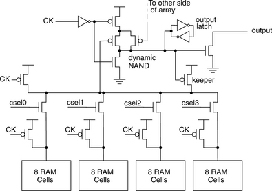
It is important to note that by having only eight RAM cells connected to each bitline, the activated memory cell can easily and quickly discharge this bitline properly, allowing the use of single-ended sensing without any penalty in access latency.
6.3.2 L2 Array Bitline Structure
The bitline structure of the L2 cache is shown in Figure 6.7. This figure shows the single-ended read implementation of the L2 cache. One out of 32 memory cells is activated by its corresponding wordline. This activated memory cell discharges the precharged bitline, forcing the static NAND to go high. In combination with an 8:1 column-select signal, the output of the NAND then discharges a set of global bitlines. Finally, an activated bank-select signal gates these values on to the output latch.
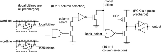
For this cache, the high degree of banking used allows the creation of multiple read and write ports that can all potentially be active as long as different banks are accessed by each. This significantly increases the bandwidth between the L1 and L2 caches, allowing effective L1 fillups to proceed faster because of the added parallelism.
6.3.3 L3 Subarray Implementation
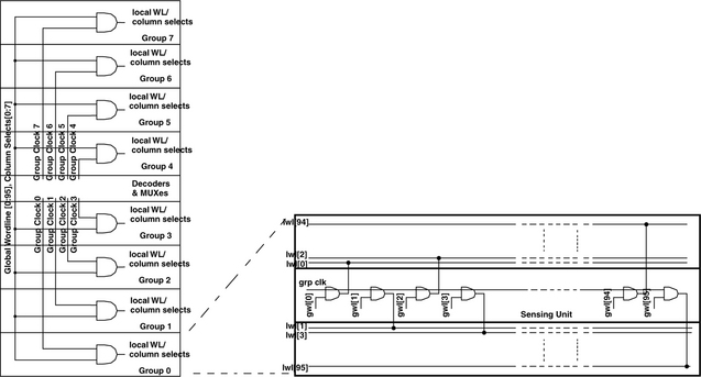
One of the techniques used in the implementation of the Itanium-2 L3 cache is the subarray technique. This method allows the cache to be built up of independent subarrays whose relative placements and operation are largely independent of one another. In this way, no exact and fixed floor plan for the L3 cache is necessary, and the subarrays can be arranged to maximize the usage of die area by optimizing the fit between core blocks, as shown in the sample floor plans in Figure 6.8 explored during the design of the cache. This is especially important for the L3 cache since it takes up the most space in the processor, and efficient use of this space is critical.

FIGURE 6.8 The Itanium-2 L3 cache subarray floor plan. (a) and (b) are candidate floor plans, and (c) shows the final die photo that implements (b). It is important to emphasize that when using this method, this kind of change can happen even during the later stages of the design cycle, something that would not be possible in most cache designs. (Pictures and diagrams used with permission from Weiss 2004).
The internals of a subarray are shown in Figure 6.9. The figure shows each subarray divided into eight groups and how decoding and sensing is accomplished within a single subarray and within individual groups.
Finally, although the subarray outputs can simply be used immediately, a faulty subarray would render the whole microprocessor inoperational. Instead, a level of redundancy and error corrections is added (5 ECC + 2 redundancy arrays for every 128 data subarrays) to maximize the yield, as shown in Figure 6.10.

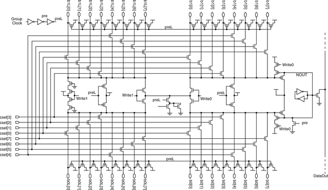
Finally, the sensing unit of a single subarray is shown in Figure 6.11. The figure shows 16 different bitline pairs. The L3 cache also uses single-ended sensing, so in a read access, only the right parts of the bitline are actually utilized (the complementary bitlines to the left are used for writes, which are still accomplished differentially). On a read access, a falling bitline chosen by one of the eight column selects pulls down the lines DATA0 and DATA1 which are connected to a PMOS-based dynamic NAND gate whose value is then latched and serves to discharge the precharged output node.
6.3.4 Itanium-2 TLB and CAM Implementation
In this section, we present a method employed by the Intel Itanium-2 in optimizing the access of its virtual-memory-enabled L1 caches. Before proceeding, we provide a background on how this L1 cache access is conventionally performed before going into details of the Itanium-2 implementation.
The use of virtual memory has become an indispensable part of modern computing. In a typical microprocessor, the caches are physically indexed and either physically or virtually tagged such that access to the cache tags and data can be started at the same time as the translation (instead of having to wait for the full translation to be done before starting the actual cache access). This translation is conventionally performed by a structure called a translation lookaside buffer (TLB), which caches the most recent virtual-to-physical address translations that have been used by the microprocessor. TLBs, in turn, are best implemented as small, fully associated memories to maximize the hit rate to compensate for their small size. This full associativity is best implemented as a special content-addressable memory (CAM). Typically, the very basic CAM is capable only of indicating the presence of the desired data and which line it is stored in. The multiple “match” signals (one per line) that are generated by this operation are then typically used as the wordline signals supplied to a conventional SRAM array that contains the actual data to be accessed. These concepts are shown and demonstrated in Figure 6.12, which shows the block diagram of the TLB access and the typical circuitry used to implement it.

FIGURE 6.12 A conventional TLB and cache read access. (a) Shows a block diagram of the cache access, including the TLB access (both the CAM and RAM parts). (b) Shows internals of a CAM cell showing the inputs being compared to the internal state of the CAM cell and discharging a “match line” during a match. (c) Shows internals of the TLB CAM and RAM access. The left part shows the N-bit address input being matched to an M-entry CAM producing M-bit one-hot match signals which are then used as the wordlines of a conventional RAM array, which produces the actual data and a match signal signifying a TLB hit.
The path described above typically lies on the critical path of most microprocessors. Speeding up a microprocessor requires that this path (among others that are also critical) be shortened. One way that this can be done on a microarchitectural level is by using a prevalidated tag microarchitecture, as implemented by the Intel Itanium-2.
The main concept behind the prevalidated-tag architecture is that instead of storing a physical address in the cache tag array and comparing this with the physical address output of the TLB, the cache tag array only contains a one-hot pointer to the TLB entry that contains the actual physical address. The main benefit behind this scheme is that the tag compare can be performed on the aggregate TLB match signals and the tag array output, removing the TLB RAM access from the critical path. Figure 6.13 shows an example demonstrating this prevalidated-tag microarchitecture.

FIGURE 6.13 An Intel Itanium-2 prevalidated-tag microarchitecture (way-O match). The cache tag arrays store a one-hot pointer to the TLB entry instead of the entire physical tag (here, Way 0 points to TLB entry 2, while Way 1 points to TLB entry 7). The tag comparison can be performed right after the access to the TLB CAM cells when the match lines are produced, instead of waiting for the actual address output from the TLB RAm. This example shows the prevalidated-tag microarchitecture for two ways, but the concept is readily applicable to caches with higher associativity.
It is important to note that although the prevalidated-tag microarchitecture speeds up the TLB cache critical path, it does introduce complexities into the system, with the main issue being the need to ensure that every pointer stored inside the tag array is properly defined as valid or not, even after changes are made to the TLB. Cache entries that point to a stale TLB entry (i.e., those that were pointing to a TLB entry that has been overwritten by a new one) must be invalidated to ensure that no false matches occur. Although this may sound like a significant problem, the fact that TLB misses occur infrequently and TLB fills themselves are expensive means that the additional cost of updating the cache to properly reflect the new TLB state can be easily absorbed during this operation—introducing additional delay to the infrequent case of TLB fills, while speeding up the common case of an access that hits the TLB.