
Sensor data acquisition systems and architectures
M.D. Todd, University of California San Diego, USA
Abstract:
This chapter describes key topics in the design and operation of conventional data acquisition systems used for structural health monitoring. These systems are discussed by four sub-system modules: (1) the sensor module, which consists of the physical element(s) that interact with the system-under-test to sense the physical process(es) and convert that information into a detectable signal form (e.g., an electrical voltage); (2) the signal conditioning module, which may have any number of functions, which could be further subdivided into analog functions (voltage amplification, some types of filtering, and possibly telemetry) and digital functions (timekeeping, digitization, triggering, master control); (3) the output module, which provides an actual indication, in an appropriate form, of the measurement(s) desired; and (4) the control module, which contains some form of an active controller that interprets the output and feeds back that information to an actuator that can manipulate the physical process (only present in active sensing systems). In the discussion of each module, the relevant hardware and signal processing components that comprise its operation and function are described, and the chapter concludes with a short summary of key concepts and observation of trends in data acquisition for structural health monitoring.
Key words
sampling; signals; analog-to-digital conversion; sensor metrics
2.1 Introduction
This book considers sensing technologies for civil infrastructure monitoring and health management, the scope of which was addressed in Chapter 1. Any such monitoring activity inevitably requires getting a measurement (more likely, many measurements) of some physically-observable behavior of the structural system e.g., the system’s vibration, strain, temperature, etc. This chapter will present an overview of important concepts related to the process of getting such measurements (‘data acquisition’), the primary issues associated with this process, and the most common architectures used to execute this process. A fairly comprehensive list of important topics in this chapter includes time/frequency domain signal analysis, probability, uncertainty analysis, analog-to-digital conversion (and digital-to-analog conversion (DAC)), sampling theory, transducer design, multiplexing/demultiplexing, filtering, and many aspects of hardware design. A number of excellent books on these subjects are available for example Kay (1993); Figliola and Beasley (2000); Doeblin (2003); Ayyub and Klir (2006); Beckwith et al. (2006); Bendat and Piersol (2010). Each of these topics warrants an entire literature collection by itself, so the primary objective of this chapter will be to present relevant information about the most important of these topics, defined to be the ones of salient interest to the engineer interested in civil infrastructure monitoring applications. As such, this chapter begins with an overview of what measurement systems generally ‘look like,’ then considers a number of background concepts in signal processing, and subsequently discusses the specific realizations of the components and their properties that comprise typical voltage-based measurement systems. The chapter then concludes with some of the differences found in digital input/ output and in optical-based measurement systems.
2.1.1 General measurement system
A very general schematic of a measurement system is shown in Fig. 2.1. The schematic shows the bridge between the physical process being detected (e.g., acceleration vibration of a structure) and the analyzer (the engineer who reads and interprets output from the measurement system) as several modules. The first module is the sensor module, which consists of the physical element(s) that somehow interact with the system to sense the physical process and convert that information into a detectable signal form (e.g., an electrical voltage). For example, in a structural vibration application, the sensing module might consist of an accelerometer mounted to the structure; the accelerometer contains an inertial mass that moves in response to the host structure motion, and this inertial mass motion induces stress in some piezoelectric material, which causes an electric potential (voltage difference) to develop.

Information from the sensing module proceeds to a signal conditioning module, which may have any of a number of functions that could be subdivided into analog functions (voltage amplification, some types of filtering, and possibly telemetry) and digital functions (timekeeping, digitization, triggering, master control). The signal conditioning module in this conception may be thought of as the ‘brain’ of the measurement system, as it is primarily responsible for taking raw information from the sensing module and converting it to a form suitable for display and analysis by the engineer (analyzer). In the accelerometer example, the signal conditioning module would contain a charge amplifier (the voltage differences produced by the piezoelectric effect are very small), a noise filter (to get rid of very high-frequency random processes), a Nyquist filter (tuned to the desired sampling frequency of the system), a multiplexing unit (for appropriately managing multiple accelerometer channels in simultaneous signal detection), some form of analog-to-digital converter, and a controller with analog or digital trigger input/output, a buffer, and a master clock. Digital data are then sent to the output module, which provides an actual indication, in an appropriate form, of the measurement. The simplest module might be a digital word read-out of the measurement value on a display, although more commonly the digitized words are stored (either in RAM or on a digital storage medium) for interface with a personal computer. The most sophisticated output modules integrate post-digitization data analysis (see Part I ‘Sensor data interrogation and decision making’ in Volume 2), usually with external software.
Finally, data from the signal processing module may also interact with a control module, which contains some form of an active controller that interprets the output and feeds back that information to an actuator that can manipulate the physical process. This module is only present in active sensing applications; in the context of the accelerometer measurement, if part of the civil infrastructure application was to mitigate excessive levels of vibration, then some sort of control module would be present whereby acceleration signals are used as feedback to, say, hydraulic dampers, to actively reduce the acceleration. This control module is not meant to be confused with a number of activities that the signal conditioning module performs in controlling the data acquisition process such as timekeeping, filter setting, and so forth; all applications will have some sort of signal conditioning module that controls the data acquisition process, but only active sensing applications will have the additional separate control module that directs actions that explicitly affect the physical process being measured.
2.1.2 Sensing module
While this chapter will focus primarily on the signal conditioning module and system-level architectures, a few words must be included on sensing. The sensing module itself depends primarily upon what physical process must be detected and/or controlled, and many of the chapters after this one treat major sensing categories in detail. One element common to all sensors is that they convert kinematic, kinetic, or thermal information to a measurable and controllable quantity, such as a voltage or current, which is then processed, either in hardware or software, to obtain information that supports decision-making e.g., structural health management. The main point here is that all sensors are themselves dynamic systems, and it is generally very useful to model their output, y(t), as such, e.g.:
![]() [2.1]
[2.1]
where F(t) is the physical process being monitored (assumed time-dependent), and the ci are coefficients that characterize the sensor. The order of the highest derivative required to accurately describe the sensor’s response to the physical input is the sensor order; as an example, consider a piezoelectric accelerometer and its equivalent dynamic system model (Fig. 2.2). If the absolute displacement of the inertial mass inside the housing is defined as y and the input to the accelerometer is defined as x, the system may be readily described by its equivalent dynamic model as:
[2.2]

and by noting that the relative motion of the inertial mass, z = y – x, is what will affect the piezoelectric element, the input/output model may be written as:
[2.3]
which directly relates the kinematic output (z) to the input (x). Clearly, in this case, the accelerometer is a second-order sensor. If the second-order case of Equation [2.1] is divided through by c0, the resulting coefficient ratios c2 / c0 ≡ 1 / ω2, which will always have units of time squared (e.g., s2), and c1 / c0 ≡ τ which will always have units of time (e.g., s), completely define the dynamic behavior of the sensor to the physical process input. Similarly, the ratio F(t) / c0, which always has units of output field units divided by input field units, defines the sensitivity of the sensor. In particular, the reciprocal 1/ c0 ≡ K is known as the static sensitivity of the sensor, and that value, along with the two previous ratios defined, determine the complete behavior of the second-order sensor.
The static sensitivity simply relates static input change to static output change, and zero-order sensors are completely characterized by this value since the higher-order constants are zero. For a zero-order sensor, such as a simple piston-style tire pressure gage, if the static pressure were F(t) = ΔP where ΔP was the pressure difference inside the gage and outside, then the sensor would read K Δ P, where by simple physical modeling one could find that K = A / k, where k is the piston spring stiffness and A is the cross-sectional area of the gage chamber.
The static sensitivity, however, does not completely characterize the input/output relationship for a dynamic signal input. Dynamic signals cause a first-order response in a sensor due to a capacitive (‘storage’) element; thus the constant τ now governs the sensor’s response to inputs. This constant is known as the time constant of the sensor, and the general solution to first-order linear sensor systems is an exponential decay. The response to any input F(t) for a first-order sensor is given by:
[2.4]
 [2.4]
[2.4]
where the sensor now has a transient response (whose duration is governed by τ) and a steady-state response that depends on the input itself (as well as τ) A bulb thermometer is an excellent example of a first-order sensor. First-order sensor responses to dynamic input are noted for a time lag before reaching steady-state (due to the time constant τ) and both phase and magnitude change between input and output (depending also upon τ).
Finally, second-order sensors, such as the accelerometer first introduced, are characterized not only by a static sensitivity and time constant but also by a characteristic natural frequency, ω, related to the second-order constant above. The general response of a second-order sensor is given by:
[2.5]
 [2.5]
[2.5]
where ξ = ωτ / 2 is the sensor’s damping value. Depending on the relative values of the parameters K, τ, and ω, a second-order sensor will either oscillate or exponentially decay to the steady-state input, with a magnitude and phase offset from the input dependent upon all these parameters. If the input occurs at time scales commensurate with ω, the phenomenon of sensor resonance occurs, where very large outputs (i.e., significantly different from the static sensitivity K) are achieved per unit input. As ω → 0 , a second-order sensor responds with static sensitivity K, as expected, but the resonant effect changes the dynamic sensitivity of the sensor significantly, effectively reducing the frequency band over which it is a useful sensor.
As a consequence of sensor module dynamics, several performance metrics are usually defined that are important to consider when selecting a sensor type for a given application. These performance metrics are summarized here:
1. Sensitivity. This is the fundamental scaling relationship that the sensor obeys in transferring input (what is desired to be measured) to output (what is actually measured). This metric is usually given by the static sensitivity K, or in the case of dynamic sensors, augmented by the time constant τ and (in the case of second-order sensors), the operable frequency band that avoids sensor resonance.
2. Cross-axis sensitivity. This metric describes how much the sensor responds to inputs not aligned with the primary sensing direction, given in the same units as the sensitivity above or possibly a fraction or percentage of the main sensitivity. Single-axis accelerometers typically have a non-zero cross-axis sensitivity, and this value can be verified by mounting the accelerometer on its side to a shaker and measuring its output per unit input.
3. Resolution. This metric quantifies the minimal detectable value of input and is usually given in terms of an amplitude or power spectral density e.g., volts2/Hz. A common way to estimate resolution is to isolate the sensor from any inputs, measure a long time history of its response to this nominally quiescent state, and compute the average amplitude or power spectral density of the time history. Bendat and Piersol (2010) describe the concept of spectral density estimation in great detail.
4. Dynamic range. This metric describes the full operating range over which the sensor behaves as intended (linearly with static sensitivity K, distortion-free, etc.) and is usually defined as a logarithmic ratio between maximum measurable value and minimum measurable value (thus expressed in decibels (dB)). Sometimes, sensor manufacturers report also a percent linearity metric, which shows how much departure from expected linear response could be expected. As a side note, while less common, dynamic range can occasionally refer to operating frequency bandwidth, some care must be taken to understand context of the value.
5. Sensitivity to extraneous measurands. This metric quantifies how the sensor responds to unintended inputs and is usually expressed as a static or dynamic sensitivity. The classic example is the thermal sensitivity of a strain gage sensor, as it is well-known that strain gages respond to thermal strain as well as mechanical strain. Accelerometers also may have thermal sensitivity that must be quantified in order either to use the accelerometer only in an appropriate temperature range or otherwise to correct the output.
These fundamental performance metrics are useful in the selection, calibration, and operation of any sensor. Fundamentally, the output from the sensor module is an analog voltage that will be sent to the signal conditioning module for suitable transformation into digital information. In the following section, some fundamental concepts in signals and sampling are presented to facilitate understanding of this module’s functionality and operation.
2.2 Concepts in signals and digital sampling
This section provides a general context for fundamental concepts in the nature of analog signals and their digital sampling. It will establish a general signal model and then review relevant sampling requirements and the representation of digitally-sampled signals.
2.2.1 Sampling criteria
The sensor module outputs y(t) are inevitably analog voltages, and while analog waveforms are continuous in time and amplitude, they do not lend themselves to easy storage and subsequent processing. Inevitably, digitized representation of the measured outputs is required, which involves appropriate sampling of the waveform. The most important sampling parameter is the sampling frequency, fs, which determines the rate at which the analog voltage is recorded; the time between each sample Δt is the inverse of the sampling frequency, or Δt = 1 / fs. Figure 2.3 shows a 1 s-long 5 Hz sinusoidal waveform sampled at four different sampling frequencies, 95 Hz, 45 Hz, 15 Hz, and 7 Hz. Each point represents the value recorded at that instant in time; clearly, the larger the sampling rate, the more closely-spaced the samples are, and the analog waveform is more accurately approximated. Clearly the sinusoid is not very accurately portrayed in either amplitude or frequency as the sampling frequency gets too low (connect the dots with straight lines in Fig. 2.3 to visualize what the engineer would observe). In the case of sampling at 7 Hz, it appears that the engineer is not even observing a 5 Hz waveform anymore, but rather something distorted at a lower frequency.

One way to better visualize what is happening is to transform the time series y to the frequency domain Y via a discrete Fourier transform (DFT),
[2.6]
where the discretized voltage y(t) is now a sequence of points yn n = 1,…, N, and the corresponding DFT is discretized at each frequency, k = 1,…, N. The time between samples Δt corresponds to a frequency width of Δf = 1/NΔt = fs/N. Figure 2.4 shows the magnitude of the DFT for each corresponding time series of Fig. 2.3. As expected, a peak is observed at 5 Hz for each sample rate that is at least twice that of the waveform; however, when the 5 Hz waveform was sampled at 7 Hz, spurious frequencies known as aliasing frequencies appear due to the fact that the sample rate is not fast enough to capture the oscillation. The Nyquist sampling criterion thus states a condition for minimum sampling to avoid aliasing: one must choose fs > 2fmax, where fmax is the highest expected frequency contained in the measured waveform. The Nyquist frequency is then defined to be half the sampling used, fN = fs / 2, and this represents the frequency above which any frequencies in the analog waveform will be aliased. If the Nyquist sampling criterion is followed, the frequencies estimated by the DFT procedure will be accurate. Otherwise, false alias frequencies will be folded back into the spectrum and interfere with actual frequencies such that they cannot be distinguished, creating false information or masking true information. The alias frequencies fa corresponding to any given frequency f are fa = |f –nfs|, where n > 0. In the case of sampling at 7 Hz, the first alias frequency for the 5 Hz waveform is |5–7| = 2 Hz, and a 2 Hz peak is observed in the spectrum. Thus, this 5 Hz waveform sampled at 7 Hz is not different from a 2 Hz waveform sampled at 7 Hz. The peak near 6 Hz is just a consequence of the symmetry of DFTs about fN. In the general (and typical) case of sampling a signal of unknown frequency content, the only way to avoid aliasing is to low-pass filter the signal with an analog filter (prior to discretization) at fN.

The waveforms of Fig. 2.3 were all sampled in such a way that the total number of samples was an integer number of the fundamental period (0.2 s), and the amplitudes predicted by the DFT were correct (the sinusoid had an amplitude of unity, and the DFT gave an amplitude of 0.5, as a full double-sided DFT will always give amplitudes at half the value, except at DC and Nyquist frequencies, due to the symmetry of the spectrum). Consider the same 5 Hz waveform sampled at 95 Hz again (well above the Nyquist criterion minimum sampling frequency) at different record lengths. Figure 2.5 shows this waveform and its corresponding DFT for different record lengths. One can see in the time series that an exact number of cycles is not being sampled, and in the DFT, distortion is appearing near the peak at 5 Hz; this is known as leakage, and it occurs as a result of the discontinuity in the waveform that the DFT effectively sees, since DFT estimation assumes periodicity of the measured waveform. Leakage may be minimized prior to digitization only by varying the desired frequency resolution, Δf, and observing statistics on the estimated waveform. The smaller the frequency resolution, the more that any leakage will be minimized. Post-discretization leakage suppression may also be performed via windowing prior to DFT estimation, whereby the discretized waveform yn is multiplied by a discrete window wn that tapers the finite data record to be zero (or at least periodically equivalent) at the boundaries. A number of windows exist e.g., a Hanning or half-cosine window wn = (l/2)(1–cos2πn / N), and an excellent detailed discussion of the trade-offs among windows may be found in Oppenheim et al. (1999). In summary, by adherence to the Nyquist sampling criterion and by varying Δf appropriately, one will obtain the best sampling frequency and record length to establish discretization of the analog waveform in terms of optimal accurate frequency and amplitude information.

2.2.2 Digitization and encoding
The process of discretization of the analog voltage waveform involves encoding the voltage in some finite, digital representation. Nearly all measurement systems employing digitization of analog data employ some variation on binary encoding, which is just a number system using base-2 (instead of the usual decimal, or base-10, system most engineers work with). Binary encoding uses the binary digit, or bit, as the fundamental unit of information, and a bit may only be a ‘0’ or a ‘1’ (only two possibilities since it is a binary-encoded system). By combining bits, numbers larger than 0 or 1 may be represented, and these bit collections are called words. Eight-bit words have a special name historically, known as bytes.
The word length – the number of bits used to comprise the word – defines the maximum number that the word can represent. The N individual bits that comprise an N-bit word can be arranged to produce 2N different integer values; for example, a two-bit word would be expected to have 22 = 4 combinations, and those four combinations are 00, 01, 10, and 11. The decimal numerical value of these words is computed by moving from the right-most bit to the left-most bit, so the decimal equivalents to these 2-bit words are 0, 1, 2, and 3, respectively. Thus, an N-bit word can represent all decimal integers from 0 to 2N–1 (e.g., a 16-bit word can represent any integer 0–65,535). The left-most bit (bit N–1) is known as the most significant bit (MSB), since it contributes the most to the overall value of the word, and the right-most bit (bit 0) is the least-significant bit (LSB). This is known as straight binary code.
Because all of the numerical values are of the same sign in straight binary code, it is a unipolar encoding. Offset binary code is a variant on this where the MSB is used as a sign, effectively converting an N-bit word’s evaluation range from –2N–1–1 to + 2N–1–1, resulting in a bipolar encoding. Thus a 4-bit word in straight binary code has an evaluation between 0 and 15, while the offset binary code for the same 4-bit word has an evaluation between − 7 and + 7. There are also ones- and twos-complement binary codes, which simply move bits around in the word to change the positioning of the zero; twos-complement encoding is very popular in personal computers. As a comparative example, the 4-bit word 1010 has a straight binary evaluation of 10, an offset binary evaluation of 2, a twos-complement evaluation of − 6, and a ones-complement evaluation of − 5. Other such encodings exist; one important variant that is often used for digital device communications is binary coded decimal (BCD). In this code, each digit individually is encoded in straight binary. For example, the number 149 encoded in BCD would be 0001 0100 1001 (a binary 1, a binary 4, a binary 9). The advantage of BCD is that each binary number has to be only 4 bits in order to span the range 0–9. As the full value of the number being encoded goes beyond 9 (say, to 10), it just engages the next higher-order word.
2.3 Analog-to-digital conversion
Given the signal model considerations in the previous section, this section considers issues associated with the digitization of these signals. The section first considers issues (such as quantization error) associated with the digitization process, and then presents fundamental analog-to-digital converter architectures in common practice.
2.3.1 Quantization and quantization error
The bits that comprise digital words may be thought of as electrical switches, where the 0 and 1 may indicate the ‘off’ and ‘on’ position, respectively. By forming words from the bits, a switch register is created that conveys the numerical of value through the various individual bit switch settings. This switch register is connected to a voltage source such that the ‘on’ position (bit value of 1) corresponds to some reference, nominally labeled ‘HIGH’ voltage (for example, + 5 V) and the ‘off’ position (bit value of 0) corresponds to a ‘LOW’ voltage (for example, 0 V). This is standard transistor-transistor logic (TTL) design, where the switch is expressed by a flip-flop circuit (Fortney, 1987). Figure 2.6 shows such a simple switch realization on the left side of the schematic. Control logic dictates whether the switch is open or closed, which consequently results in either a HIGH or LOW reading at the switch output. The middle part of the schematic shows a 4-bit switch register specifically showing the binary value 1001 (the MSB and LSB are HIGH, and the two interior bits are LOW). The right side of the figure shows the actual output voltage series, where each output is sampled at the sampling time Δt specified. This is the fundamental architecture by which electrical devices indicate binary code.

The analog voltage outputs from the sensor module must be encoded into the binary form for further processing, as just described. The basic process is called analog-to-digital (A/D) conversion. and this conversion is generally some form of quantization. A/D converters are designed to operate over some voltage range, VR. Typical designs include unipolar converters between 0 and 10 V or bipolar converters between − 10 to + 10 V or even − 25 to + 25 V. An N-bit A/D converter, as described in the encoding discussion of Section 2.2.2, produces N-bit words that can convey 2N total binary values between 0 and 2N–1. Thus, the resolution Vres of the A/D converter is just the ratio of total available voltage range divided by total available digital range, or
[2.7]
Consider a 0–4 V unipolar, 3-bit A/D converter. This device will have a resolution Vres = 0.5 V, which means that errors may occur between the actual input voltage and the binary encoding of that voltage by the A/D converter. For example, an input voltage of 0 V would result in the same binary encoding as 0.45 V (namely 000), yet an input of 0.51 V (much closer to 0.45 than 0 V) would result in a higher binary encoding, 001. This is called quantization error, and thus the resolution of the converter represents the value of its LSB. Figure 2.7 shows the A/D conversion process for this A/D converter. The resolution is 0.5 V, so the binary output is constant for 0.5 V increments in the input voltage. A common design tool is to spread quantization error symmetrically about the input voltage, as opposed to the biased way Fig. 2.7 indicates. As such, a bias voltage equivalent to ½ LSB is usually added to the input voltage internally within the A/D converter so that the error (in this example) would be ± 0.25 V. The dashed line shows ideal conversion for comparison; clearly, as Vres gets smaller, ideal conversion is asymptotically achieved.

Wagdy and Ng (1989) derived a formula for the variance of the quantization noise, which depends on the magnitude of the signal (assumed harmonic), here expressed somewhat differently as a fraction α of the A/D resolution Vres
[2.8]
 [2.8]
[2.8]
where J0 is a zero-order Bessel function of the first kind. For signals that are large compared to the resolution (the most common scenario), i.e., α ![]() 1, the summation term drops out, and the variance approaches the usual variance associated with a uniform probability distribution over the resolution range, Vres2 / 12. The quantization-limited signal-to-noise (SNR) ratio in dB for a harmonic signal that fills the entire available range is given by:
1, the summation term drops out, and the variance approaches the usual variance associated with a uniform probability distribution over the resolution range, Vres2 / 12. The quantization-limited signal-to-noise (SNR) ratio in dB for a harmonic signal that fills the entire available range is given by:
[2.9]
 [2.9]
[2.9]
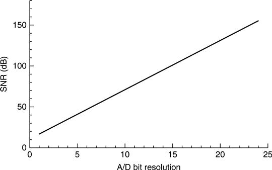
Equation [2.9], for sufficiently large signals, is plotted in Fig. 2.8; each bit adds about 6.02 dB of SNR capability. Most converters in today’s A/D markets are at least 16-bit, resulting in a quantization error nearly 100 dB below a unit signal. Increasingly, 24-bit converters are becoming more and more common.
At small signal levels (α small), distortion can happen due to the nonlinear dependence upon the signal (Equation [2.8]), and this distortion comes after any anti-aliasing, so the detected signal may have significant degradation. One common remedy for minimizing distortion is by dithering. Dithering is a process where random noise at least twice the amplitude of Vres is deliberately added, and the effect is to ‘noise shape’ the quantization error in such a way that the distortion is eliminated at the expense of slight SNR decrease. Most A/D systems automatically dither input voltage signals.
Errors can also occur at the extremes of the voltage range of the A/D. If the input voltage drops below 0 V, the A/D converter is low-saturated and will continue to encode the voltage as 000 regardless of the actual input voltage. Similarly, if the input voltage goes above 4 V, the A/D converter is high-saturated and will continue to encode the voltage as 111 regardless of the actual input voltage. These saturation errors result in the familiar phenomenon of clipping in the observed digital time history; a clipped zero-mean sinusoid would have flattened peaks for the portions of the trace that exceed the A/D voltage range.
2.3.2 Analog-to-digital converter architectures
A number of different designs for implementing the general A/D conversion (ADC) process described above exist (Kester, 2005). Four are in most common practice: Flash ADC, Successive approximation ADC, Ramp converter ADC, and Sigma-delta ADC. Flash ADCs are known as direct ADCs, as they have a series of comparators that sample the input signals in parallel in the switch register, resulting in very fast direct voltage encoding (on the order of GHz sampling rates), but typically are low-resolution (e.g., 8 bits or less), because the number of comparators needed doubles with each required bit, resulting in very large circuits.
Successive approximation ADCs, one of the most common methods, estimate the input voltage essentially on a trial-and-error basis, as the name suggests. A comparator is used to reject voltage ranges, finally settling on the proper voltage range through a feedback circuit from a digital-to-analog converter (DAC) (discussed later) that provides the guess from a shift register. The sign of the comparator essentially chooses which bit value to converge to per clock cycle. Unlike Flash ADC, each bit desired requires one clock cycle, so an 8-bit successive approximation ADC would require eight times longer to obtain an 8-bit word than the Flash ADC. However, the quantization noise is better controlled, and successive approximation ADCs are much less costly to build. As such, the cost/speed trade-off has favored their deployment for many commercial systems.
Ramp converter ADCs generate a sawtooth (piece-wise linear ramp) voltage signal and use a comparator, integrator, and capacitor (sample/hold) network to discern the input voltage level. A clock governs the voltage ramp changes, and the time is noted when equality occurs. Ramp converters have, typically, the least number of logic gates, and the approach results in some of the highest accuracy, particularly for low signal levels (sub-millivolt). However, the local oscillator used to generate the ramp is often sensitive to the ambient thermal environment, and its linearity (and thus accuracy) can be compromised. Ramp converters are relatively slow due to the oscillator as well, although some nonlinear ramp converters have been implemented that reduce the sample/hold latencies (Figliola and Beasley, 2000).
Finally, sigma-delta ADCs simply oversample the input voltage significantly, filter the desired measurement band, and convert at a much lower bit count via Flash ADC. This signal, along with any quantization error from the flash, is fed back into the filter, and this has the effect of suppressing the noise of the flash. Then, a digital filter is applied to downsample the flash conversion, remove unwanted noise, and increase resolution. Sigma-delta ADCs are primarily digital devices and are very cost-effective and energy-efficient, and this type of ADC is particularly common in audio digital media (CD, DVD).
2.4 Digital-to-analog conversion
In many measurement applications, particularly if there is a control module, and even in the design of some A/D systems (see previous section), there is a need to convert digital information back to analog information (D/A conversion), e.g., most commonly a voltage. The simplest way to envision most DAC is shown in Fig. 2.9, where a 4-bit DAC is drawn. The network consists of four resistors having a common summing junction, with each resistor doubling in size starting at the MSB. At the operational amplifier output, the voltage Vout is easily computed to be
[2.10]
 [2.10]

where the bn is either 0 or 1 depending on the n-th bit value that controls that switch. A clock controls when each bit value is latched until the next clock cycle, and the effect is that the current Vout is held during that cycle; this results in a piece-wise constant output, similar to the A/D quantization in Fig. 2.7. This ‘stairstepping’ results in some potentially unintended high harmonic content being generated, which must be analog filtered before the waveform is sent to whatever device requires it. This is very important to understand if the DAC is being used to generate precise control inputs for feedback purposes.
2.5 Data acquisition systems
A data acquisition system (DAQ) is the intégration of several components within the signal conditioning module, the sensing module, the output/display module, and sometimes the control module that leads to stored, manipulable digital data representations of the sensor measurements. This integration is accomplished in a compact DAQ board that easily interfaces with a personal computer. A very general schematic for DAQ systems used for centralized wired-sensor configurations is shown in Fig. 2.10, where a single central controller is assumed.

2.5.1 Analog signal considerations
Analog sensor voltages are sent first into a conditioning unit that could serve several purposes. One of the first subcomponents in this unit is a bank of shunt circuits; the actual raw output from many sensors (e.g., piezoceramic accelerometers) is a current rather than a voltage, and a shunt circuit uses Ohm’s law to convert this current to a voltage suitable for use with the DAQ system. DAQ systems either have separate current/voltage inputs or switches that engage shunt circuits in analog input channels when needed. Not all voltages from the sensors, however, are suitable for the voltage limitations (VR) of the DAQ components (such as the ADC). Thus, many analog voltage signals need either amplification or attenuation to avoid the saturation effects shown in Fig. 2.7. Amplifier gains in most modern DAQ systems are controllable individually on each channel via switch logic that engages variable resistor banks (for amplification) or engage variable resistor voltage divider networks (for attenuation).
The specific form of the wired connections to the DAQ unit typically are either single-ended or differential. Single-ended connections use one line from the sensor as the active input to the amplifier and reference the other to ground, which must be common for all of the analog sensor channels. The common ground point is external, usually provided by the DAQ board. If all the sensors cannot be wired to common ground, or if a separate ground source exists at some source point (power supply for the sensors, for example) that cannot be common-grounded, the possibility for a common-mode voltage exists, which will combine unpredictably with the true input signals to cause interference. Conversely, differential-ended connections allow voltage differences to be measured among variably-grounded sensors and/or other voltage sources. Here, the second sensor line is attached to the amplifier without any ground junction, and the voltage measured is the difference across the amplifier; hence it is often called a ‘floating’ measurement because it is not measured relative to a fixed ground. Differential connections are usually required for systems taking in many diverse voltage/current sources, and they have the ability to measure very small voltage signals more accurately, provided a large resistor is dropped between the amplifier’s second input and ground. Most modern DAQ boards allow software-programmable switching between single-ended and differential conditions as the specific measurement situation warrants.
After voltage conditioning, analog filtering is another very common action. Although not present on all DAQ boards, anti-aliasing filters with cut-off frequencies set to the Nyquist frequency, as described in Section 2.2.1, remove irrelevant high-frequency information that could wrap into the measurement band. In customized systems, special analog filters that serve to either high-, low-, or band-pass the voltages, may be present in the design prior to sampling and digitization. For conventional strain gage or other resistance-based sensors, special resistor bridges (e.g., a Wheatstone bridge) may be present for noise rejection, and for thermocouple temperature measurements, cold-junction compensation units may exist for measurement stabilization to as low as 0.25 °C.
After signal conditioning, each sensor output has to be multiplexed. Multiplexers are basically integrated circuits that use parallel flip-flops to rapidly select individual lines and pass along the information, allowing a multi-channel system to share common telemetry and ADC. This drastically reduces cost in DAQ systems. The trade-off for some applications is that inevitably there is an interchannel delay induced by the multiplexer as it individually selects each channel, leading to lags in the absolute synchrony of data recorded across several channels. True simultaneous sampling may be achieved without a multiplexer, but as long as the inter-channel delay is negligible compared to the overall sampling frequency, the phase errors that result will also be negligible. Finally, the analog data are sent to the ADC for digitization, as already described in detail in Section 2.3.
A central controller, or central processing unit (CPU), governs the entire DAQ process, as shown in Fig. 2.10, and its primary functions are timing control and information buffering, including often interfacing with some form of external personal computer, although these controllers can operate independent of a personal computer. The CPU’s processing speed depends on its internal clock speed and the design of the various buses in the DAQ system. Buses are just electrical pathways through which information and commands are sent among the CPU, memory, the ADC, any other peripherals including digital input/outputs, and the personal computer. Most DAQ systems have a central bus through which many other devices/components interact through other buses. Figure 2.11 shows such a schematic. Essentially, the central bus contains three information pathways: an address lane, a data lane, and a control lane. As data are to be moved around the DAQ system, the address lane contains a digital description of the locations of the two components between which the data are to be exchanged (‘Where are we going to and coming from?’), the data lane contains the data information itself (‘What data are going or coming?’), and the control lane contains the status information regarding logistics and control of data movement (‘How and when do we send the data?’). When data, or information, are being sent over the central bus, the control lane sends a ‘busy’ flag so that other information flows do not interfere, and a ‘ready’ flag when the process is finished; in this way, the same lanes may be used for many different types of operations that execute at different speeds. This is called ‘handshaking.’

Memory is a mechanism for data and information storage and retrieval, and, regardless of specific type, basically consists of registers for storing digital information. Most memory types are classified as either non-volatile (does not require power to retain/store information) or volatile (does require power to retain/store information). Common types of non-volatile memory include basic read-only memory (ROM), flash memory, and older personal computer peripheral magnetic storage devices (e.g., floppy disk or zip disk). ROM is physically unchangeable information (microcode) typically used in firmware or hardware for dedicated processes. Flash memory is a very common storage mechanism today because it may be easily erased and reprogrammed via dense NAND or NOR gate architectures (both functionally complete logic gates, meaning any binary operation may be performed by combining NAND and/or NOR gates). Flash is found in common universal serial bus (USB) flash drives, solid state external hard disks, smart phones, and audio/video systems. Some DAQ systems employ flash memory in assisting the transport of data across different devices with different speeds, known as buffers. Buffers consist of some pre-allocated memory storage space where data may reside without interruption to other system processes until the receiving device sends a ‘ready’ flag over the control lane. Data stored in most buffers follows a first-in, first-out (FIFO) protocol, where data that were the first to enter the buffer are also the first data to leave, preserving the original ordering of the data.
One important class of non-volatile memory is the electrically-erasable programmable read-only memory (EEPROM). Unlike flash memory, which cannot effectively be overwritten in small (byte-level) amounts, EEPROMs are large arrays of floating-gate transistors that may be modified (written to) by increasing the voltage levels as determined by the user. Modern EEPROMs have a life cycle measured near 106 reprogramming cycles, and this often is the design limit for systems that use them. EEPROMs are used in DAQ operations for functions such as device configuration and complex, varying computation on post-digitized data.
Volatile memory is typically classified as either static random access memory (SRAM) or dynamic random access memory (DRAM). The terms ‘static’ and ‘dynamic’ fundamentally differentiate between whether the semiconductor needs to be periodically refreshed (dynamic) or not (static). Each bit in SRAM requires four cross-coupled inverting transistors for storage and two more transistors for control; conversely, DRAM stores each bit on a capacitor with a single transistor for control, but the capacitor needs periodic recharging (hence, the term ‘dynamic’). Thus, DRAM footprints are much smaller and allow much denser circuit design, resulting in significant cost savings; DRAM is subsequently the most common memory type found in personal computers. However, SRAM uses less power, does not suffer some of the bandwidth limitations that DRAM does, and is much easier to interface over buses; so many DAQ systems employ SRAM architectures for some memory requirements.
2.5.2 Digital communications
Much of the multifunctionality that is required for modern DAQ systems has been integrated into compact ‘plug-and-play’ boards. Figure 2.12 shows a generic schematic of such a multifunctional plug-and-play board. These boards contain several analog and digital communications, processing, and control functions. As already seen in Section 2.5.1, digital signals play a critical role in a number of CPU, control, triggering, signal processing, and A/D operations in a DAQ system. Generally speaking, digital (TTL-compatible) signals communicate with devices in serial (bit by bit) or in parallel (in words).

Standards have been established by which these digital communications are achieved. One of the fundamental serial communications standards was RS-232C, originally used for telephone/modem communications. This protocol allows for either 9-pin or 25-pin connections for two-way communications via two single-ended lines (transmit, or T/X, and receive, or R/X) and a ground line. The remaining wires are related to handshaking. The data are sent in successive streams, one bit at a time, where each bit is represented by an analog voltage pulse, with 0 and 1 being represented by a voltage of opposite polarity (usually in the 3.2–25 V range). Transmission streams generally are composed of a start bit, 7–8 information bits, a parity bit (sometimes), and a stop bit; the start and stop bits work together to execute proper handshaking. Parity just involves counting the number of 1’s in a word, and the addition of a ‘1’ as a parity bit makes the number of 1’s predetermined either even or odd. Some devices can effectively do simple error checking by checking for the parity bit. A newer serial standard suite, RS-422A (with further standard modifications), allows for 37 differentially-connected pins for noise reduction and uses 0 V and + 5 V signals for 0 and 1, respectively. Up to 255 devices on a single RS-485 (one of the later modifications of RS-422A) could be accommodated, with 2 million bit/s (2 Mbit/S) transfer rates over 50 m cable lengths.
A more modern (and now, far more common) serial protocol is the USB, which has become the standard in personal computers. The USB architecture is a tiered-star topology (hubs and branches), allowing up to 128 devices to interconnect between 1.5–12 Mbit/s over 5 m cable lengths (version 1.0, 1995). A host computer might connect to a root hub on which up to four other devices may be connected, including other hubs that them-selves can have daughter device connections (hence, the ‘tiered-star’ terminology). Each individual cable configuration consists of two data wires: a power wire and a ground wire. The USB standard allows in situ enumeration and initialization when a USB device is connected to a host or hub, allowing instant digital communications without powering anything down. The host directs all traffic routing through the tiered-star network. In USB 2.0 (2000), speeds were significantly increased to 480 Mbit/s and improved sleep/wake performance for connected devices (better power management). USB 3.0 (2008) brought speeds up to 4 Gbit/s and has been appearing since 2010 in some host personal computers and peripherals. Beginning with USB 2.0 and increasing with USB 3.0, DAQ architectures have increasingly used this protocol for communications, particularly with personal computers serving as hosts.
In addition, parallel communication protocols have been in use for dedicated instrument buses. By far the most common and widely-accepted standard was IEEE-488, the General Purpose Interface Bus (GPIB). GPIB is an 8-bit parallel bus. The bus uses eight ground lines and 16 signal lines, eight for bi-directional data transfer, three for hand-shake, and five for bus management. GPIB, however, was not really intended for direct connection to personal computers for the multifunctional DAQ capability implied by the schematic in Fig. 2.12, and other bus designs were developed. One of the most common is the Peripheral Component Interconnect (PCI) bus, first introduced in 1992, with 58 or 60 pin connections, depending on specific architecture. General specifications included 33 MHz clock with synchronous (parallel execution) transfers, a 32-bit bus width, and either 32-bit or 64-bit memory address space. PCI-X was developed as a newer parallel bus in 1998 with up to 533 MHz clocks.
PCI-E (also known as PCI-Express) was developed as a serial bus in 2004 that substantially improved throughput (16 GB/s in a 16-lane bus) and reduced the number of pin connections, since it is based on point-to-point topology; a 4-lane PCI-E bus has the same peak transfer rate as a 64-bit PCI-X device (both about 1 GB/s), but the PCI-E will ultimately perform better when multiple devices are transferring data, due to the serial architecture. Parallel bus architectures, particularly when loaded fully, suffer from timing skew, which is the phenomenon whereby parallel signals transmitted simultaneously arrive at their destination at slightly different times due to the unique length of each signal’s path.
2.6 Optical sensing DAQ system
Sections 2.1–2.5 have presented overviews of the relevant signal processing and hardware architectures used in most conventional, wired DAQ systems that interrogate sensors inherently producing voltage or current analog waveforms that are proportional to the physical field being measured. Optical sensing inherently takes advantage of modulated properties of light – intensity (power), wavelength, polarization state, or phase – to deduce changes to the measured field. In fiber optic sensing architectures (the kinds used most commonly for structural health monitoring applications), the light is completely contained, until detection by a photo-detector; in an optical fiber, a cylindrical waveguide that uses refractive mismatches to exploit total internal reflection and coherently propagate the light over very long distances (km in the case of infrared-wavelength light). In this way, fiber optic sensing strategies are self-telemetered; the ‘power source’ and the sensing mechanism are contained within the fiber, which makes for far less cabling and electronics equipment required near the sensing field itself. Additionally, since all information is optical at the sensor sites, the susceptibility to extraneous measurands is often reduced, particularly in the case of electromagnetic interference. Three fiber sensing references with specific application to practical sensing considerations include the comprehensive Lopez-Higuera (2002), Yeh (1990), and Todd (2005).
Chapter 5 considers specific optical sensing architectures in greater detail, but fundamentally almost every fiber optic sensing approach requires (1) a source of light generation, (2) exploitation of some optical property modulated in a fiber, and (3) photodetection. Thus, fiber optic DAQ requires both optical components and non-optical components, and Fig. 2.13 depicts a general fiber optic sensing schematic. Depending on the sensing principle, light is generated by a laser (narrowband) or diode (broadband), transmitted to the sensing regions of the fiber where sensing is accomplished via intensity, phase, or wavelength modulation, and the modulated light is detected by a photodetector. A piezoelectric element may be present for some sensing architectures in order to control a tunable optical filter on the optical side. Photodiodes, photodetectors, and tunable filters will be discussed in turn.

2.6.1 Photodiodes
Semiconductor-based optical sources are a very common and practical choice for most sensing applications, mainly due to their compactness, long service life, and relatively low cost. This section will be limited to light-emitting diodes (LEDs), although laser diodes are very commonly used as well. Light emission in LEDs is based on electron transition from an occupied state in the conduction band to an unoccupied state (hole) in the valence band, which is called spontaneous emission: the electron–hole recombination process is a radiative process that emits a photon. This process is only possible if occupied states in the conduction band have the same wavenumbers as holes in the valence band. This is not an equilibrium state, and pumping of electrons from the valence band to the conduction band is required from some external source. Because semiconductors are also susceptible to absorption processes (where a photon transfers its energy from a valence band electron to promote it to the conduction band), the electron-pumping rate must over-come this to achieve a positive gain. The non-equilibrium state required to achieve emission is stimulated by voltage-biasing a p-n junction diode. The electrical field produced by the bias voltage induces electron drift from the n-side to the p-side and hole drift in the opposite direction. At the junction region, where concentrations of electrons and holes are very high, recombinations promote spontaneous optical emission in all directions, and even stimulated emission once an optical field is produced. A variety of materials and substrates have been employed to produce light at wavelengths from as low as 400 nm up to 25 000 nm; typical materials include In, Al, Zn, GaASP, or InGaAs with GaAs, GaP, or InP substrates. The optical bandwidth of the emissions depends on wavelength and temperature and typically ranges between 30–150 nm. Since each spontaneous emission event is uncorrelated, so are the emitted photons with respect to phase, direction, and polarization. With surface-emitting diodes, photon emission is through the substrate, perpendicular to the junction (see Fig. 2.14a). The substrate is etched, and a circular ring acts as the contact with the fiber placed as closely as possible to the active emission region. With edge-emitting LEDs (ELEDs), light is emitted from the side (parallel to the junction), which results in higher extraction efficiency (Fig. 2.14b). ELEDs are better for long-distance, higher bit-rate transmission, but they are more sensitive to temperature fluctuations than surface-emitting diodes. Typical maximum optical power outputs, depending on wavelength region, vary from about 0.015–8 mW.

2.6.2 Photodetectors
In 2.6.1, the concept of spontaneous emission was mentioned in conjunction with the operating principle of LEDs. The reverse, but very similar, process is absorption, where incoming photons transmit their energy to valence band electrons that subsequently are promoted to the conduction band. This is the process behind the operation of photodetectors, which may be defined as devices in which photons are converted to electric charge carriers. The effect of the electric charge carriers is measured by applying voltage with a load resistor to generate a current. The amount of current generated by the electric charge carriers is often called the photocurrent, but even when no light is incident upon the device, a current is still produced by the polarization circuit (called the dark current). This feature should be kept as low as possible for SNR optimization. The primary performance metric of photodetectors is the responsivity, defined to be the ratio of the output photocurrent (in amperes) to the power of the incident light (in watts). Responsivity is a function of both the incident optical wavelength and the device’s efficiency at converting the light to current. Different materials respond with different efficiencies across the optical wavelength spectrum, and in some cases, they do not respond at all. The materials typically used in photodetectors are Si, GaAs, Ge, and InP, similar to LEDs.
One common type of photodetector is a p-i-n photodiode, as shown in Fig. 2.15a. This device is very similar to the LED structures presented previously, except that an intrinsic semiconductor is inserted between the p and n layers. In addition, these layers have been highly doped (denoted by ‘+’ signs in the figure), which increases the electric field in the transition zone and reduces the concentration of minority carriers. A reverse bias voltage is applied (on the order of a few volts) to establish the polarization current. Reverse bias photodetectors are inherently very linear devices with regard to responsivity over wide dynamic ranges (up to 60 dB) up to saturation, which typically occurs at about 1 mW of input power. Typical fiber sensing systems as well as communications applications do not require nearly this high a power level, so saturation is rarely an issue. The performance of the photodiode is most affected by the thickness of the detector active area and the detector time constant.

A second type of photodiode is the avalanche photodiode (APD), shown in Fig. 2.15b. The overall structure is similar to a p-i-n photodiode, but a large reverse bias (on the order of hundreds of volts) is applied that causes the electrons generated by the photon incidence to accelerate as they move through the active region. These carriers tend to collide with other electrons, inducing some of them to join the photocurrent, initiating an avalanche process that continues until the electrons are outside the active region. This process results in a large gain factor that multiplies the responsivity; this gain factor may be increased by increasing the reverse bias voltage, but this is done at the expense of increased dark current (and thus noise). Furthermore, since not every electron undergoes the same avalanche multiplication, this becomes a source of noise, so a limit is placed on the usable gain factor. The same factors that affect the design of the p-i-n photodiode affect the APD, with the additional time required to execute the avalanche multiplication process. Trade-offs between using p-i-n photodiodes or APDs depend on the relative importance of responsivity, resolution, stabilization requirements, and cost. APDs have internal gain due to the avalanche effect, so they are more responsive, but have higher noise properties. Since this gain factor also depends on temperature, thermal compensation is almost always required for proper use of APDs. In addition, APDs cost more and have much larger voltage and stabilized source requirements than p-i-n photodiodes.
2.6.3 Tunable optical filters
Wavelength-specific acceptance or rejection (filtering) of light propagating in a fiber has many sensing applications, particularly if wavelength is used as a multiplexing strategy in a sensor network. Tunable, in-line filtering is realized mostly with resonator cavities such as a fiber Fabry–Pérot (FFP) tunable filter. The most commonly used form employs a fiber-coupled Fabry–Pérot tunable filter as a bandpass filter. Tunable FFPs make use of a Fabry–Pérot etalon, shown schematically in Fig. 2.16. Two fiber ends with partially reflecting dielectric mirrors implanted inside are brought some distance d together with an air gap between them. When light is incident upon this gap, multiple reflections will be established, and the reflections will constructively or destructively interfere dependent upon the spacing d (and the wavelength λ) For an incident optical wave, the phase delay it undergoes after each round trip is given by ϕ = 4πnd / λ, where n is the refractive index in the gap. If the mirrors have the same transmission T and reflection R properties, the transfer function H of the ratio of the power transmitted out of the etalon to the incident power is given by:
[2.11]

where a 360° shift, not explicitly shown, is assumed accrued at each reflection boundary (dielectric reflection boundary condition), and scattering losses have been ignored. This function is plotted as a function of phase angle for various values of R in Fig. 2.16. The transfer function has pi-periodic windows of maximum transmission with a transition sharpness dependent upon the reflectivity. The larger that R is, the sharper the transmission peaks will be.
Two performance metrics for FFPs are important: the free spectral range (FSR), or the distance between transmission peaks, and the finesse, defined to be the ratio of the FSR to the full width of the transmission peak at half of maximum value (FWHM). These metrics are typically expressed in terms of the wavelength, so conversion from phase to wavelength is employed through Equation [2.11]. They may be summarized by:
[2.12]
 [2.12]
The finesse is only dependent upon the reflectivity of the mirrors. For filtering applications, a wide FSR may be desirable, but this also implies a wider bandwidth for a given finesse, which is undesirable for sensing applications. Commercial FFPs typically have FSRs between 40 and 80 nm (at 1550 nm), passband bandwidths of about 0.2–0.5 nm, and a finesse of 100–200. The tunability of the passband center wavelength is controlled by varying d, which is typically done by incorporating a piezoelectric element with voltage control at the micron-level of displacement (Fig. 2.16). Such filters are used in a variety of fiber Bragg grating-based and interferometric-based sensor architectures, both of which are discussed in greater detail in Chapter 5.
2.7 Conclusion and future trends
This chapter presented an overview of important concepts related to the process of obtaining and processing measurements of relevant kinematic or kinetic behavior of structures, the primary issues associated with this process, and the most common architectures used to execute this process. Specific focus was placed upon conventional, wired data acquisition processes for making voltage measurements. A fairly comprehensive list of important topics in this chapter included time/frequency domain signal analysis, filtering, probability and uncertainty analysis, analog-to-digital conversion, DAC, sampling theory, transducer design, multiplexing/demultiplexing, and important sensor-level and system-level aspects to selecting DAQs for a given application. This chapter also presented an overview of digital data acquisition (including common protocols such as USB) and presented common architectural components for fiber optic-based data acquisition (with far more detail on this topic presented in Chapter 5 of this book). The references provided at the end of this chapter were carefully selected to provide more information in each of these topical areas. The objective of this chapter was to give an engineer tasked with a structural health monitoring application the most relevant information required for obtaining voltage-based measurements (and fiber optic measurements, to some degree), understanding how they get processed in preparation for conversion into useful information, and the issues and challenges associated with such data acquisition.
While the conventional wired data acquisition architectures and fiber optic sensing architectures discussed here certainly still dominate most structural health monitoring applications, primarily due to their proven reliability, robustness, and regulation certification acceptance where required (such as the aerospace industry), there are a number of trends in data acquisition that are substantially advancing the field. First and foremost, beginning in the 1990s, was the wireless revolution. Key data acquisition components described in this chapter (D/A, A/D, signal processing) were integrated with microcontrollers, software/firmware ‘micro’ operating systems, and wireless antennas into much smaller platforms called nodes. Chapter 15 describes the general architectures of wireless nodes, and gives some deployment examples, but the primary revolution in this advancement was taking data acquisition from a centralized construction (where each sensor’s raw data are streamed individually over wires to the central acquisition/processing unit, where A/D, demultiplexing, sampling control, and appropriate signal processing are governed) to a distributed construction, where each sensor node now may perform many of these operations locally and wirelessly broadcast reduced information sets rather than raw data (decreasing band-width requirements and providing potential redundancy in the information movement chain).
Somewhat concurrent with this wireless trend, fueled by the telecommunications industry’s development of smartphones in the mid to late 2000s, is a trend toward low-power components (powered at 0.5 V and operating in the mW range, compared to powered at 5–10 V and consuming several W). As data acquisition components achieve lower power usage requirements, energy harvesting strategies (Chapter 17) become much more feasible, and as such energy harvesting – defined to be any strategy that seeks to convert otherwise wasted or unused non-electrical energy sources into useful electrical energy – has become a big research and development topic. In particular, since wireless sensor nodes require a local power source such as a battery, energy harvesting could provide alternative means of powering such nodes to create an energy-neutral platform with increased autonomy. Not surprisingly, autonomy in general has been another important sensing/data acquisition trend, and Chapters 13 and 14 discuss some important developments in robotic and vision-based sensing that support this trend. In fact, it is becoming increasingly clear overall that sensing and data acquisition are moving toward increased autonomy, increased intelligence, and even sensor system self-awareness and adaptability. Figure 2.17 shows this taxonomy, evolving from where the field has been (centralized architectures) to the current state-of-the-art (hierarchical and decentralized) to the near future (self-assembled, self-aware, cooperative networks) and even beyond (mimicry of complete socio-ecological systems). These very advanced sensor networking and programming concepts are, at the time of writing, very much at the cutting edge of sensor network research and development.
