
Laser-based micro- and nano-fabrication of photonic structures
Abstract:
The development of photonic micro-systems requires advanced and robust lithographic methods, which enable the reliable fabrication of intricate, high-quality, three-dimensional (3D) structures at high spatial resolution. In this context, the laser is presented as a versatile tool for fabrication and rapid prototyping beyond the limitations of earlier methods. Supported by the growing availability of tailored and efficient photo-sensitive materials, laser lithography builds specially designed multidimensional photonic micro- and nano-structures for emerging M(O)EMS/N(O)EMS applications. Laser-based fabrication methods for two-dimensional (2D) and 3D photonic structures and application examples are presented, whereas a special focus is put on two-photon absorption-based laser lithography, related material and technological aspects.
6.1 Introduction and motivation
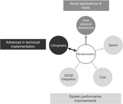
Photonics – the management of light – is a key technology today for the benefit of mankind (Photonics21, 2010). The utilization of light comprises the generation, detection, amplification, processing and control over propagation and polarization of light. In photonic applications the concerted use of light is based on the interaction of light and matter, which is generally accompanied by a change of the properties of light (direction, flux, polarization, wavelength, etc.). While a simple medium influences light mainly by intrinsic material properties, periodic geometric arrangement of media with different refractive indices enables new possibilities. However, such structures require wavelength-sized features for a strong light–matter interaction. Thus, miniaturization plays an important role on the one hand improving integration, speed, cost and performance of multidimensional photonic systems, and on the other hand facilitating new physical phenomena such as light confinement and redirection by photonic bandgap structures (commonly known as photonic crystals), enhanced transmission in metal films and artificial materials (with both negative electric permittivity and negative magnetic permeability, so called left-handed materials). With respect to the technical implementation of photonic systems, miniaturization motivates additionally novel and advanced lithographic methods (Fig. 6.1). Multidimensional photonic architectures and state-of-the-art fabrication methods are comprehensively reviewed in the literature (cf. Arpin et al., 2010; Busch et al., 2007; Jahns et al., 2008).
With respect to micro- and nano-optics and the integration of optics into micro- and nano-optical and electrical systems (MOEMS/NOEMS), patterning by means of photolithography (and associated etching processes) has greatly and adapted and led the way to improved lithographic processes as exemplified in Section 6.2. The technical implementation of more sophisticated lithographic methods, which enable the direct 3D integration of optical structures, opened novel applications and systems not only in microelectronics, but also in micro- and nano-photonics and extended to other fields such as medicine, MEMS fabrication, micro-fluidics and biology.
6.2 Fabrication of 2D and 3D photonic micro-structures
6.2.1 Photolithography
The progress of miniaturization and development of photonic structures is closely related to advances in various lithographic methods (Fig. 6.2). Photolithography was a pioneering task for microscale patterning. It was originally developed for mass fabrication in micro-electronics and is progressively being used for the fabrication of optical and mechanical devices. The earliest methods for fabricating micro-optics were based on adapting the well-known integrated circuit wafer processes, which were developed for large-scale fabrication of micro-electronics, to produce wafer form micro-optics such as diffractive optical elements and lenses (Borek et al., 2007). The use of alternative exposure tools with shorter wavelengths combined with technical resolution enhancements (e.g. immersion technique or phase shift masks) and improvements in the illumination system (e.g. micro-lens arrays based light homogenization) increased the achievable resolution of mask-based photolithography and hence the field of application towards further miniaturization (Voelkel et al., 2010). The limitations of photolithography to expose only planar substrates have recently been circumvented by efforts to extend photolithography to non-planar surfaces using computergenerated holographic masks (Maiden et al., 2005).
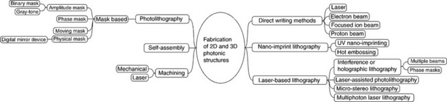
Conventional photolithography transfers a pattern from a mask in a single exposure step to a photosensitive material. The mask itself is either a binary or gray-tone mask used for the generation of either binary or locally variable exposure patterns in contact, proximity or projection mode. Other approaches are gray-tone or half-tone (mask) photolithography (Reimer et al., 1997), moving mask lithography (Hirai et al., 2007; Kim S.-K. et al., 2011), and mask-less photolithography based on digital mirror devices (Guo and Dong, 2010).
The use of dangerous or toxic agents during material processing in photolithography, special ambient conditions (e.g. yellow light, clean room, inert atmosphere conditions), pushed the adaptation of lithographic fabrication methods and triggered additionally the development of alternative structuring technologies and new materials.
A comparison of 3D micro-fabrication methods has been made (Jang et al., 2007) distinguishing between self-assembly approaches, construction-based approaches and the interference lithography approach. Self-assembly techniques are based either on block copolymer self-assembly or colloidal self-assembly. The laser as exposure tool is found in the construction-based approaches such as layer-by-layer manufacturing (such as micro-stereo-lithography), direct laser writing methods including single and multiphoton techniques as well as in the interference lithography approach, which requires the overlay of multiple coherent beams either provided by sophisticated optical arrangements in the experimental setup or by phase masks.
6.2.2 Mechanical machining
In addition to photolithography, mechanical machining is today another approach to fabricate photonic components because of the technical improvements in the achievable precision. Single point grinding and polishing as well as ultra precision diamond machining is used especially for high quality aspheric or freeform optical surfaces and prototypes. Dimensions and surface quality (roughness) depend on tool, material and machine parameters. Diamond machining can be used for machining parts with dimensions in the range of a few microns with a roughness typically in the range of a few nanometers and a form deviation in the sub-micrometer range. The positioning accuracy of the machine is usually better than the achievable structure resolution in the micrometer range due to the brittle fracture mechanism associated with the material removal process (Borek et al., 2007). The flexibility regarding complex 3D shapes of multi-axes machines is an advantage, though mechanical machining remains a time consuming and hence expensive technology. However, it is well suited for the fabrication of single parts or molds for replication. Examples of fabricated microoptics are multi lens arrays, micro-mirror arrays and fiber-coupling lenses (Gläbe and Riemer, 2010).
6.2.3 Replication methods
Less expensive but precise polymer replicas of expensive micro-optical structure can be done by injection molding or by hot embossing. In contrast to injection molding, hot embossing creates micro-structures with lower internal stress and is applied to the fabrication of micro-lenses, Fresnel lenses, optical waveguides, optical benches, optical gratins, micro-spectrometers, and distributed feedback structures for organic semiconductor lasers (Worgull et al., 2010).
Nano-imprint lithography (NIL) is a fast and cheap process for the replication of structures with features down to a few nanometers, which makes this method very attractive for mass production. A crucial factor in NIL is the quality of the stamp. High quality stamps are processed by other lithographic methods such as direct writing methods or laser-based lithography. A typical work flow of the combination of direct writing laser rapid prototyping for micro-optical elements and replication is shown in Figs 6.3 and 6.4. The replication of photonic structures in the visible spectral range requires stamps with nanometer scaled features. While direct writing methods are suitable for irregular and arbitrary patterned stamps, periodic patterns are processed defect-free over large areas by means of laser interference lithography. Subsequent replication via nano-imprint lithography yields photonic structures, for example LED applications (Kim et al., 2007).


6.4 Replicated sawtooth structure. The structure is made with a poly-dimethylsiloxane (PDMS) mold in Ormostamp according to the process in Fig. 6.3.
Two-photon-based laser lithography is used for the fast fabrication of 2D structures that are subsequently molded into PDMS in order to obtain a flexible inverse replica (Yang et al., 2004; Yi et al., 2004b). Beyond that, two-photon polymerized 3D structures can be replicated rapidly and with high quality by means of micro-transfer molding (LaFratta et al., 2004). This method facilitates the replication of structures with high aspect ratios and re-entrant features with large overhangs. This kind of soft lithographic replication of 3D structures can be extended to the fabrication of freely moving components by means of so-called membrane assisted micro-transfer molding (LaFratta et al., 2007).
6.2.4 Laser-based lithography
Laser-based lithography takes advantage of unique properties of laser radiation, such as high monochromaticity, coherence, directed emission of radiation and excellent beam quality along with high focusability. In a photolithographic approach, the laser may replace a conventional light source and provide high power radiation at a short wavelength or it can be tightly focused and used for patterning without masks. The large coherence length facilitates the generation of complex intensity patterns at sub-wavelength resolution, which can be transferred into a suitable material. Thus, there are manifold approaches for laser-based lithography for structuring a variety of materials. The laser power is used either for removal (e.g. ablation, milling, drilling and cutting), joining (welding), marking or addition (e.g. laser cladding, sintering) of material. These types of laser machining generally work on a macroscopic scale in combination with robots and may not be called lithography, but on a microscopic scale, the laser is used the same way, probably at lower power and different laser parameters, but still the laser deposits energy in a target material, which is then patterned. This microscopic and macroscopic direct patterning or writing process can be called laser lithography in the classical meaning of lithography.
Different laser sources (Table 6.1) have been widely used for laser precision macro-, micro- and nano-machining (Chong et al., 2010) and optical lithography for various transparent materials such as glasses or polymers. Although local melting of glass by means of CO2 laser heating results in the formation of glass lenses (Veiko et al., 1986), laser direct writing of microlenses in soda-lime glass is achieved with an Nd:YVO4 laser (Nieto et al., 2010) or intense UV laser exposure (355 nm) leads to glass swelling and the formation of superficial glass bumps (Logunov et al., 2011); femtosecond lasers are especially versatile instruments for processing. Thus, fs lasers are widely used in micro- and nanotechnology for the precise ablation of metallic and transparent materials (Gattass and Mazur, 2008; Kazansky et al., 2004; Kondo et al., 2004) and laser engineering of biomaterials (Stratakis et al., 2009). Intense ultrafast laser pulses can induce structural and/or optical changes, and nonlinear effects, such as multiphoton ablation or multiphoton absorption. Regarding microscale patterning, laser-based photolithography based on multiphoton polymerization is well suited for the fabrication of 3D polymeric photonic structures without the need of layer stacking as in other lithographic methods, which require time consuming sequential alignment and processing.
Table 6.1
Some important laser types, emission characteristics and field of application
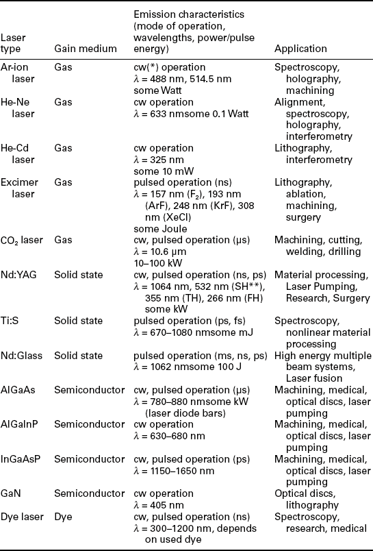
Notes. Cf. Bäuerle (2008).
(*)cw = continuous wave
(**)SH = second harmonic; TH = third harmonic; FH = fourth harmonic.
In micro-fabrication, the laser represents a powerful tool for patterning and is used as a flexible (in terms of wavelength, pulse width, etc.) light source in laser-assisted (photo-) lithography. In this context, excimer lasers have been widely used as described in Section 6.2.1 due to their high photon energy and high output power, which can be technically exploited by efficient laser-ablation processing of many different materials. But with the technical use of the intense light of a femtosecond laser, an alternative light source entered laser-based lithographic processes, which is capable of processing a large variety of materials, ranging from metals to transparent dielectrics for diverse applications (Fig. 6.5).

Femtosecond laser pulses are used for the ablation of metals and dielectrics (2D and 3D structures), structural changes of materials, optical changes or mechanical processing such as cutting, drilling or milling in order to replace mechanical machining tools. The power of ultrafast lasers is sufficient to efficiently process hard materials such as steel (e.g. NAK80), which is a common material for molding in the plastics industry. Setting the power close to the material-dependent ablation threshold, structures with sub-diffraction limited features can be generated, fine enough to show color effects (Noh et al., 2007). Moreover, the direct writing of 2D and 3D conducting structures can be realized by laser-based decal transfer of Ag silver nanopaste on a substrate, which can replace electrical bonding of electro-optical chips in micro-systems (Wang et al., 2010). Another way of generating a direct laser-written structure is the laser-assisted diffusion of interstitial ions in semiconductor heterostructures for the generation of sub-micrometer LEDs (Makarovsky et al., 2010).
Furthermore, intense ultrafast laser pulses can trigger nonlinear effects such as multiphoton ablation or multiphoton polymerization in a photosensitive resin via photo-initiation and photo-polymerization. There are many different approaches to how a laser can be used to build a physical structure: the focusing of an intense laser pulse may result in evaporation of material from a target (laser ablation), which uses the laser in a machining way to replace diamond tools for drilling, cutting or milling. High power lasers are used in rapid prototyping of 3D structures to melt powder-like materials selectively (selective laser sintering – SLS) or induce a photochemical reaction, which alters material properties used in laser-based photolithography. In most cases, the laser focus acts like a laser-pencil, which moves in a defined way (i.e. according to a template) across the target and writes a 2D or 3D structure in the material. Generally, the structure is built by the energy transfer from the laser to the material, which induces a material modification at the exposed locations. The efficiency of this process depends on the material chemistry, laser intensity, wavelength, pulse width, spectral width, beam profile, repetition rate, material absorption, focusing optics, etc.
Other related methods use the laser in a number of ways for the deposition of material from gaseous, liquid and solid precursors. The techniques involve either laser-induced chemical/electrochemical or physical reactions, which subsequently deposit a material on a substrate. Material transfer methods use a laser for removal of the transfer material from a substrate to another receiving substrate in close vicinity. These methods such as laser chemical vapor deposition (LCVD), laser-enhanced electroless plating (LEEP), laser-enhanced or activated electroplating, laser consolidation of thin solid films, laser-induced forward transfer (LIFT), matrix-assisted pulsed laser direct write (MAPLE), laser-induced backward transfer or laser contact-free trapping and transferring of particles in solution for 3D direct writing are surveyed in Hon et al. (2008). Each method can be treated extensively, which is clearly beyond the scope of this chapter, but not all of them are used in the field of photonics. The next section is dedicated to the most relevant methods related to the laser fabrication of photonic structures.
Direct writing methods take advantage of a patterned energy deposition from scanning an energetic beam over a sensitive material. Common scanning beam lithographic methods are electron beam lithography (Steingrüber et al., 2001), focused ion beam lithography (Callegari, 2009), proton beam lithography (Bettiol et al., 2004; Debaes et al., 2006; Sum et al., 2004; van Erps et al., 2010) and laser lithography (Rhee, 2010).
Two- or multiphoton or laser-based lithography has been applied as a versatile tool in micro-fabrication for optical, medical and biological applications (see below). Because of the high spatial resolution and the 3D structuring capability, the two-photon technology can be used for 3D data storage. Examples of photonic micro- and nanostructures are presented in below.
6.3 Laser lithography for the fabrication of photonic structures
Optical lithography benefits from the high throughput due to parallelism in fabrication and hence low device costs. It is the work-horse in modern semiconductor industries. But it suffers from the diffraction limit imposed by physical optics, which is proportional to the wavelength of the light source and the numerical aperture of the imaging optics. Decreasing the wavelength from ultraviolet to deep ultraviolet opened the path for excimer lasers to become useful light sources in lithographic work stations. A simultaneous increase of the numerical aperture based on immersion technology further pushed the achievable critical dimensions for patterning to lower values. State-of-the-art values for numerical aperture (1.35), wavelength (193 nm) and taking advantage of resolution enhancement technologies such as phase shift masks, off-axis illumination, optical proximity correction and improved resists decreased the value for the critical dimension from 500 to 45 nm. Multiple exposure techniques further decrease the wavelength and hybrid lithography, which combines, for example, 157 nm interference lithography and electron beam lithography, may ensure that optical lithography remains of crucial importance (Rothschild, 2010).
Some aspects related to the laser fabrication of photonic components are presented in the next section.
6.3.1 Ultraviolet, deep ultraviolet and laser photolithography
Laser light sources in the ultraviolet spectral range are either frequency multiplied solid-state lasers or gas lasers. Especially excimer lasers provide pulsed high power ultraviolet to deep ultraviolet emission at a typical repetition rate of a few hundred Hz up to some kHz. The main scientific and industrial applications of excimer lasers are material processing, lithography and medicine, involving methods such as laser ablation, engraving, marking, surface and sub-surface modifications and coatings made via pulsed laser deposition in either projection or direct exposure mode. In projection mode, the laser light is projected via a mask onto a target for UV exposure. In direct exposure mode, the focused laser light directly ablates the material by moving the focused laser across the target. In projection mode the effect of the laser results either in patterned material removal or in exposure of the material without removal, which depends mainly on the laser fluence and applied pulse number.
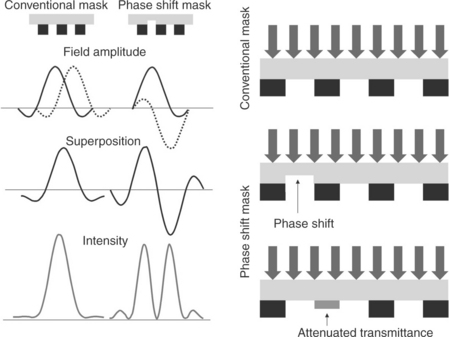
The active medium of an excimer laser is a gas of electrically excited dimers (‘excimer’, or more precisely excited complexes), where an excited noble gas atom and a halogen form a noble gas halide, which decays after a short time (typically some ns) into the dissociated state (e.g. Kr*F →Kr + F) under emission of UV light. The type of excimer determines the wavelength of the emission. The technically most relevant excimers are ArF, KrF, XeCl and XeF (Basting et al., 2002) and there are manifold applications for excimer laser processes such as excimer-based optical lithography (Elliott and Ferranti, 1989; Partel et al., 2010), excimer laser chemical vapor deposition (Wang et al., 1996), μ-fluidics (Shin et al., 2006), laser annealing of thin silicon oxide films (Richter et al., 2011), photochemical welding of silica micro-spheres (Okoshi et al., 2009), excimer laser micro-machining (Chiu and Lee, 2011; Ihlemann and Rubahn, 2000; Wu et al., 2006a) and eye surgery (Vossmerbaeumer, 2010). The high photon energy of the excimer radiation is capable of directly breaking intramolecular bonds of the target material, with only negligible thermal impact on the surrounding material. In 1989 KrF and ArF lasers demonstrated the fabrication of 0.4–0.5 μm feature sizes via direct photo-ablative decomposition and conventional latent image exposure with subsequent wet chemical development of deep UV resists (Elliott and Ferranti, 1989). In 1996, KrF lasers operating at 248 nm were available for lithography at stable conditions up to 1 kHz. At this wavelength such lasers were accepted tools for the manufacturing of structures with features down to 250 nm. At the time ArF lasers operating at 193 nm had not reached the same level of technical maturity, especially at kHz repetition rate, because they suffered from energy instabilities. But they were promising for lithography due to the shorter wavelength (Pätzel et al., 1996). Besides decreasing the illumination wavelength, further efforts reaching for enhanced resolution and high fidelity patterns are improvements on the illumination system, such as off-axis illumination, where the laser beam hits the mask at an angle with respect to the optical axis of the imaging system. The imaging system acts as a low pass spatial frequency filter, which introduces imaging errors such as corner rounding and line-end pullback. Different types of off-axis illumination are easily implemented by special apertures in the illumination path and often combined with optical proximity correction which improves the imaging of dense features (cf. Fig. 6.6 and 6.7). Recently, freeform lenses were developed for application in off-axis illumination (Wu et al., 2011). The use of phase shift masks for sub-wavelength lithography (Fritze et al., 2003) for contrast enhancement on the resist, and double exposure methods (Geisler et al., 2008; Mosher et al., 2009) combined with phase shift masks (Fay, 2002) or immersion technology (Yoshino et al., 2010) are other approaches for resolution enhancement. A micro-optical beam homogenizer for the mask illumination improves the achievable spatial resolution due to reduced diffraction and aberration effects (Partel et al., 2010).

6.6 Principle of off-axis illumination and optical proximity correction (Fritze et al., 2003).
KrF excimer lasers have been used for micro-structures in polymers for more than 20 years. The excimer laser machining directly from CAD files using ablation with mask projection was used for the rapid prototyping of micro-structures with optimized parameters for wall angle, ablation depth and stitching methods in polycarbonate samples (Mutapcic et al., 2005). Originally for binary micro-structures such as holes, trenches, pores or gratings, excimer laser etching and replication was applied to the field of micro-fabrication of 3D microtopologies with a contour mask technique. Non-binary topological structures with a smooth or continuous height profile can be processed by either line scans with a specially designed contour mask or gray-scale mask projection lithography (Zimmer et al., 1996). Both methods require a homogeneous beam profile, stable laser, and a good quality mask, because a controlled etch depth is achieved by the local transmittance of the mask and the number of applied pulses. Usually the homogeneous beam profile is achieved with micro-lens-based fly-eye integrators.
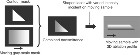
In the contour mask approach, the laser is projected via a stationary contour mask on a moving sample. Contour mask and sample motion are adapted to the desired topology and the specific ablation rate of the KrF laser pulses. Thus, point-like pulsed ablation with a specific ablation rate yields in intersecting scans the desired topology, which is shown for prismatic structures (Braun et al., 1998). The time consuming excimer ablation process is followed by a replication process using acrylates, which facilitates several tens of replications at high accuracy. Hence, a combination of both processes increases throughput of the fabrication process. It is claimed that an in situ built debris layer and its interaction with the formed ablation plume above the processed region during material ablation causes an elevated temperature of the material, which supports the smoothness of the surface. For even more complex topologies the contour mask method is combined with a moving gray-scale mask, whereas the scanning speed of the contour mask and the sample have to be adjusted in a certain ratio according to the magnification of the projection lens (Fig. 6.8). 3D topologies can also be achieved with a two-step machining approach with a diagonal scanning method and two contour masks and a third aperture mask (Zimmer et al., 2000).
For optical/photonic applications, a high surface quality after laser treatment is essential. The application of UV or deep UV laser for material ablation is an efficient method, but also highly disruptive to the target material. Thus, residual significant surface roughness is a major issue for optical applications of laser-ablated materials. Nevertheless, laser-ablation methods in combination with suitable processing schemes are used for precise etching of fused silica for refractive and diffractive micro-optics. The suggested laser-induced backside wet etching process yields direct machined surface of almost optical quality with a surface roughness of less than 10 nm rms, whereas the machined surface of the transparent sample is in direct contact with a laser light absorbing liquid. Smooth surfaces can be achieved by control of the ablation rate, which was in the range of several nm per laser pulse (Zimmer and Böhme, 2005). Other approaches yield aspheric lenses with a 248 nm KrF laser applying a planetary contour scanning method (or respective motion of the mask). This method facilitates precise surface profile control (Chiu and Lee, 2011).
Recent applications of excimer lasers in nano-fabrication cover also excimer laser-assisted nano-imprint lithography, where the laser is used as heating source to selectively melt a polymer material, which is immediately imprinted. The laser pulse heating requires a transparent stamp (fused silica), but reduces the duration of the imprint process to a few hundred ns because the imprint resist is directly heated from the laser pulse. Additionally, selective melting of resist material is proposed to remove fabrication defects and reduce the roughness, which leads to an enhancement of the structure profile. A single pulse exposure melts only a very thin layer of the surface, whereas the surface tension in the liquid phase will smooth out rough edges and reshape fabricated nanostructures depending on the experimental boundary conditions. Metal nanoparticle monolayers and periodic arrays of nanoparticles as well as sub-10 nm nano-fluidic channels were demonstrated (Xia et al., 2010). The laser-assisted imprint process is well suited for the fabrication of nm period gratings. The selective melting leads to a reshaping of fabricated squares to spherical structures, which could act as micro-lenses.
In addition to advanced optical lithography, excimer lasers are used in medical applications. The high UV power of these lasers is well suited for laser ablation of hard and soft tissue in dentistry and surgery (Murray and Dickinson, 2004). Especially ArF laser at 193 nm are used in ophthalmology for refractive corneal surgery. Due to the absorption maximum at 193 nm of the cornea, this wavelength is well suited for the removal of tissue from the cornea surface thus correcting the refractive power of the human eye. The photo-ablation leaves surrounding tissue unchanged and yields precise patterns, thus making the excimer laser a perfect tool for micro-surgery (Vossmerbaeumer, 2010).
Based upon laser ablation or surface modifications, excimer lasers are applied to fabrication of photonically relevant structures: spatially selective oxidation of silicon monoxide layers by ArF excimer laser annealing under oxygen atmosphere is reported in Richter et al. (2011). The conversion from SiOx (x ~ 1) to SiO2 is observed by increasing transmittance upon multipulse irradiation below the ablation threshold. Thus, patterned changes of transmittance and refractive index can be achieved, which is technically relevant for phase masks or patterned surface functionalization. Depending on the oxygen concentration, either smooth films for optical phase elements with a smooth surface and variations of the refractive index are obtained, or, in an oxygen-rich environment, submicron sized SiO2 nanoparticles are fabricated. In contrast to the non-ablative annealing process, excimer laser ablation lithography is used for the fabrication of gratings on various glasses (Dyer et al., 1996), binary reflective (Flury et al., 2003) or transmitting multilevel (Winfield et al., 2000) diffractive optical elements. The reflective binary diffractive optical elements are fabricated by laser-ablation lithography with excimer lasers and subsequent metal film coating. In a pixel by pixel scan across the target, a photoresist is ablated from the substrate by projecting the laser beam on the resist. In a following etching step, the pattern is transferred to a substrate and coated. This binary reflective kinoform can be used for high power laser beam shaping optics. The multilevel transmitting diffractive optics in glass were obtained by direct excimer laser ablation. In this process, a square aperture was imaged to a glass target and material was removed from the surface pixel by pixel until the desired depth was achieved.
It can be observed in glass targets that below the ablation threshold, the incident laser power leads to a local temperature increase (sub-threshold incubation), which can be measured by the deflection of a monitoring laser beam. The monitoring beam is guided parallel to the surface and focused above the laser irradiation zone. The duration of the deflection increases upon the start of ablation of material from the surface. This way, the material-dependent laser threshold for ablation can be measured. Depending on the material, the laser wavelength and a given laser fluence below the single pulse ablation threshold, incubation may occur and lead to ablation after a certain number of pulses, but incubation does not necessarily happen in all materials (Dyer et al., 1996). Incubation is considered to play a role in various polymer blends, which influences the ablation results upon excimer laser irradiation (Kunz et al., 1998). The interaction between the UV laser and the target depends on the spectral material absorption and thermal conductivity (along with pulse duration) and is thus governed by the predominance of either photochemical ablation or photo-thermal ablation, which then relates the laser-induced ablation to optical and mechanical parameters of the target material (Desbiens and Masson, 2007).
Both types of ablation play an important role in UV laser irradiation but differ depending on the polymer material. The irradiation induces a pressure jump in polymer materials and the creation of small molecules. UV lasers are used for the ablation of polymer materials, but are also useful for the transfer or deposition of polymer or other sensitive materials via pulsed laser deposition (Lippert, 2009).
6.3.2 Laser-assisted deposition methods
In addition to simply removing the material from a substrate via laser ablation, there are processes (laser chemical vapour deposition, laser-induced transfer methods, pulsed laser deposition, etc.) where the laser is used for the patterned deposition of materials on a substrate. Laser chemical vapour deposition (LCVD) was used for the in situ fabrication of micro-lenses with precise control of film properties (Wang et al., 1996). This process takes place in a reaction chamber, which contains precursor gases and the substrate. The laser is used to locally heat the substrate, which subsequently dissociates the gas precursor and a thin film deposits on the substrate. Using multiple beams or a layered approach to build the structure, it is possible to create 3D structures. The deposition rate of LCVD depends linearly on the precursor gas pressure and the laser power density and decreases with increasing scanning speed. The deposition rate can be adjusted by these parameters and is much higher than in conventional CVD (Hon et al., 2008). In a similar method (liquid-phase chemical laser-assisted deposition) an XeCl excimer laser irradiation was used for the local deposition of Pd layer from a precursor solution to form mirrors on fibre core end faces. The Pd deposition is followed by electroless copper plating in order to yield the final mirror. A subtractive method for the mirror fabrication was compared to the additive method: the laser was used for removal of the metal film around the fibre core after chemical plating of the fibre end faces, but it was found that the adhesion of the mirrors made by the subtractive method was poor compared to the additive method (Kordás et al., 2002).
Sensitive materials that are easily destroyed by the laser are often embedded in a matrix material that absorbs the laser energy. This method (matrix-assisted pulsed laser deposition, MAPLE) uses a frozen solvent, which is evaporated upon laser irradiation. The material for deposition is evaporated together with the matrix and deposits on a receiving substrate. Without masks, the material deposition is unpatterned, hence another method, laser-induced forward transfer method (LIFT) is often used for laser-assisted patterning (Fig. 6.9). Pulsed laser deposition methods, ablation mechanisms and applications are discussed in Schneider and Lippert (2010). In the LIFT process, the laser energy is absorbed in a thin film on a transparent substrate, which leads to evaporation of the transfer material. Subsequently, the evaporated material precipitates on a second receiving substrate, which faces the first substrate in close (micrometer) vicinity. For soft-matter materials such as polymers or biological compound materials, a direct contact between the substrates was found to yield the best transfer results regarding resolution and defined edges of transferred pixels (Palla-Papavlu et al., 2010a, 2010b).

LIFT can be achieved with various types of lasers (UV excimer lasers, Nd:YAG, Ar-ion lasers, fs lasers). The transfer materials are often sensitive to oxygen or humidity, thus requiring a vacuum or inert gas setup. Originally used for the patterned transfer of metal films, it can be applied for a variety of materials including oxides and biomaterials or even more complex multilayer systems such as a polymer light emitting diode pixel (Shaw Stewart et al., 2011) or organic thin film transistors (Rapp et al., 2011). Such sensitive materials or materials which are transparent to the incident laser or easily destroyed by the incident laser, can be transferred by using an energy absorbing sacrificial layer (dynamic release layer (Shaw Stewart et al., 2010) between the transfer material and the carrier, which promotes the release of the material. Additionally, the temporal shape of ultrafast laser pulses influences the LIFT process and the achievable resolution on the receiving substrate, which is attributed to fast electron and lattice interactions. It was shown that fs pulses with a short separation (less than 500 fs) show large impact of the deposited pixel size, while the covered area stays constant for longer pulse separations up to 10 ps (Papadopoulou et al., 2010).
Using microsphere arrays as micro-lenses, parallel material transfer (parallel LIFT) with an unfocused laser beam can be achieved (Othon et al., 2008). The polystyrene beads are on top of a transparent substrate (quartz glass) and focus the incident light onto the single or multilayered transfer material, which is on the other side of the substrate. Thus, micron to submicron holes can be written into the films and corresponding dot patterns on the receiving substrate.
6.3.3 Laser interference lithography
Instead of scanning a focused laser beam through a photosensitive material, laser interference lithography (LIL) is very well suited for the fabrication of various types of nanoscale structures (Xie et al., 2008). It has been used for the fabrication of nanostructures in various fields and with many different technical approaches and is comprehensively reviewed in the literature (Jang et al., 2007; Xia et al., 2010). Here, only some basic issues of this technology are summarized.
LIL is capable of structuring rather large areas in a single shot exposure or limited exposure time without defects and without scanning, but is limited to periodic patterns. The fabrication of a 4 × 4 cm2 photonic crystal using a holographic element in combination with a mask is reported in Zhang et al. (2006). The large holographic element comprises three separate gratings (each rotated by 120°) and generates four transmitted beams (first diffraction order from each grating plus transmitted centre beam). The incident laser beam is expanded to a diameter of 20 cm and the exposure of the positive type resist for the photonic crystal fabrication is 3 min.
The laser provides light of defined wavelength, polarization and coherence, thus enabling coherent superposition of multiple laser beams, whereas the experimental conditions such as laser fluence, film thickness, angle of incidence and polarization of the beams directly correlate to the fabricated patterns. The periodicity (or the lattice constant of the unit cell) of the pattern is determined by the difference between the wave vectors of the interfering beams and is thus proportional to the wavelength of the laser and the angle between the interfering beams, which are crucial and limiting parameters for the achievable spatial resolution. The shape of the image formed within a unit cell of the pattern is influenced by the polarization of the beams and its position within the unit cell depends on the initial phase difference of the beams. The laser intensity, exposure time and development procedure also have an impact on the final pattern shape. Depending on the number of beams (N), angle between the beams and polarization, 1D, 2D and 3D (maximum N – 1) periodic patterns can be fabricated over a fairly large area in a single exposure step. Multiple exposure steps with rotation and translation of a 1D phase mask facilitate complex 3D patterns such as woodpile structures with three beams (Xu et al., 2010). The coherence length limits path differences in the optical setup and determines also the maximal area that can be processed in a single exposure step. The coherence length of the used laser determines whether wave front splitting or amplitude splitting of the laser beam (Marconi and Wachulak, 2010) is used in the optical setup. The beam superposition leads to the generation of stable interference patterns, which can be used for patterning films of (usually) positive type photoresist (Ellman et al., 2009), negative type resist (Stankevicius et al., 2011), TiO2 gel films (Wang et al., 2011), hybrid organic–inorganic sol–gel materials (Della Giustina et al., 2011), biomimetic tissue (Daniel, 2006), as well as PEDOT-PSS (Lasagni et al., 2009), a conducting polymer, which is important for organic (opto)electronics (cf. Fig. 6.10).

6.10 Dual beam laser interference lithography – optical setup for balanced and unbalanced transverse beam coherence. A balanced setup requires the same number of reflections in the two interferometric paths in order to overlay same transverse beam parts.
Unwanted reflections from the substrate surface may degrade the interference patterns and lead to undercut phenomena, which can be reduced by anti-reflection coating of the substrate or thermal post-exposure treatment of the sample to induce thermal diffusion and redistribution of the photo active compound, which is applied in order to improve sidewall profiles and line edge quality and eliminate undercut features of fabricated structures. This is crucial if the fabricated structures are used as molds for subsequent nano-imprint lithography (Jang et al., 2010).
Various types of laser sources such as Nd:YAG lasers at 266 nm (fourth harmonic) or 355 nm (third harmonic) (Lasagni et al., 2011) are used for interference and holographic lithography, for which some use a laboratory setup with a more exotic wavelength in the EUV (46.9 nm) based on a capillary discharge-pumped excitation scheme that produces an intense amplification by the excitation of Ar+8 ions (Marconi and Wachulak, 2010). Regarding costs, large area LIL with semiconductor lasers seems more attractive. The AlInGaN laser has a rather low price and a long coherence length, which is a prerequisite for processing large sample areas (Byun and Kim, 2010). Recently, LIL was combined with multiphoton polymerization in a four-beam setup for the fabrication of micro-lenses. The four beams were generated using a diffractive optical element and a diaphragm to remove undesired laser light from the optical path. The negative type resist was exposed to multiple laser pulses, which facilitates much faster processing as compared to multiphoton-based direct laser writing, which is a sequential voxel-by-voxel buildup process. Appropriate hatching or stepping of the exposed area enables the processing over large areas and reduction of the structure degradation at the edge of the exposed area due to the spatial intensity profile of the laser beams (Stankevicius et al., 2011).
Since LIL requires multibeam arrangements and stable control of laser parameters for intricate intensity patterns of interfering laser beams, sophisticated and complex optical setups are required. The use of the phase mask (which actually can be fabricated by LIL) technology correlated to the desired structure is a more stable experimental approach rather than large optical setups that suffer from alignment inaccuracies or vibrations. The diffracted beams from such a mask are inherently phase-locked and provide a stable beam superposition (Xu et al., 2010). Nevertheless, multiple-beam LIL is compatible with automatic and cost-effective industrial processes beyond manual laboratory configurations and usage. An interference module facilitates the automatic setting of beam number, angles of incidence and polarization in order to obtain different interference patterns. The exposure area can be stepped over larger sample areas such as 3 inch Si wafers (Rodriguez et al., 2009). Originally used for regular 2D patterns, interference lithography is increasingly applied to 3D structures such as photonic bandgap structures with increasing structural complexity. Photonic applications taking advantage of the LIL capabilities and the combination of LIL with replication methods involve the patterned arrangement of quantum dots (Lu et al., 2009), where a three-beam configuration LIL is used for the fabrication of pore structures in SU-8, which are subsequently immersed in a solution containing CdSe/ZnSe quantum dots. The quantum dots are then dragged by capillary forces into the pores yielding a patterned luminescent architecture that could be useful for LED-based lighting applications. Further optical applications involve the fabrication of structures for enhanced light out-coupling from light emitting diodes (Kim K.-R. et al., 2011) as well as broadband anti-reflective coatings in the visible spectral range with sub-wavelength conical structures to reduce the reflection well below 1% (Ting et al., 2009) or with an extended wavelength range (250–1200 nm) and wide incidence angles up to 50° (Chen et al., 2010). Regarding such photonic fabrication processes, LIL is often used for the generation of regular master structures that are subsequently used as a mold for the fabrication of a photonic crystal-like structure diode by nano-imprint lithography on light emitting or on flexible substrates such as foils (e.g. PET films), which facilitates roller lamination, exposure through the substrate and the use of Ni shims (roller imprinting).
A simple optical setup such as Lloyd’s mirror setup for dual beam interference requires a sufficient temporal and spatial coherence of the laser beams, since the wave front of the incident beam is divided and coherently added with itself after travelling different optical paths. Folding of the wave front at the mirror requires good transverse and longitudinal spatial coherence. An interferometric setup using a beam splitter or a phase mask for the generation of the interfering beams is more relaxed in terms of spatial coherence, since two phase-locked replicas of the wave front are divided in amplitude at the splitting element and each section of the interference pattern is achieved by the superposition of the same beam section and is therefore spatially coherent (Marconi and Wachulak, 2010).
The use of micro-prism arrays in combination with interference lithography enables the fabrication of nanoscale sub-structures in micro-structures due to the complex interference patterns of the beams, which are refracted from each micro-prism. With this method, micro-particles with nanoscale sub-structures can be fabricated and subsequently released from a substrate. Such particles, showing enhanced fluorescence sensitivity, can be suspended in solutions and used for sensing (Lee et al., 2009).
6.4 Laser lithography based on one-, two- or multiple-photon absorption
The accurate fabrication of 3D structures at high spatial resolution requires alternative approaches to photolithography without the need for vertically stacking multiple planar layers with a finite thickness. A stacked 3D structure that is fabricated by a sequence of exposure steps suffers generally from limited alignment accuracies of the masks between the subsequent exposure steps. Furthermore, the creation of smooth 3D topologies requires a local variation of the exposure dose. While direct beam writing methods are more flexible than mask-based fabrication due to their inherent capability of varying the exposure dose as a function of the beam position, such methods are often used for the generation of a continuous relief in the target material (Fu and Ngoi, 2001). Although a local variation of the exposure dose in photolithography might be achieved by the use of expensive graytone masks with a sophisticated transmission profile, it is not an easy task, even for binary masks, to fabricate a mask with the desired transmittance and requires sophisticated pixel coding in order to achieve the desired number of gray levels. Nevertheless, gray-scale lithography can be applied to the fabrication of smooth micro-optical elements such as lenses (Cui et al., 2003).
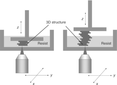
A special technique of direct write laser lithography that overcomes these problems is 3D laser lithography (3D-LL) based on multiphoton absorption, which is reviewed in this chapter. Recently, Misawa and Juodkazis (2006) edited a very comprehensive book about 3D laser micro-fabrication. 3D-LL is a true 3D method that has definitely reached a level of technical perfection over the last few years and may potentially replace other direct writing methods, such as electron beam lithography in a wide field of applications. 3D-LL based on two- or multiphoton polymerization has been applied as a versatile tool in micro- and nano-fabrication (Anscombe, 2010; Farsari et al., 2010; Fourkas and Baldacchini, 2004; Maruo and Fourkas, 2008; Ostendorf and Chichkov, 2006; Schmidt et al., 2007a, 2007b; Serbin et al., 2004; Sun and Kawata, 2004; Yi et al., 2004a, 2004b). The 3D-LL technique has been used in the following ways: for 3D structures with arbitrary shapes (Fig. 6.11), with freely moving components (Sun et al., 2000) such as photo-driven micropumps and micro-sensors (Lin et al., 2004), micro-needles, periodic and scaffold structures for photonic and biomedical applications (Ovsianikov, 2007a, 2007b), designable refractive micro-lenses (Guo et al., 2006) and pyramids (Satzinger et al., 2008), embedded photonic structures such as line gratings (Guo et al., 2003), 3D optical memory (Nakahama et al., 2005; Walker and Rentzepis, 2008), waveguides (Langer and Riester, 2007; Stampfl et al., 2009), waveguides in a flexible PDMS matrix (Infuehr et al., 2007), waveguides coupled to photonic crystal structures (Serbin and Gu, 2006), diffractive optical elements (Chen et al., 2007), photonic bandgap structures, photonic heterostructures and meta-materials (von Freymann et al., 2010), optical cloaking (Ergin et al., 2010), polymer templates for metallic structures (Gansel et al., 2009; Rill et al., 2008), flexible structures for biological cell culture studies (Klein et al., 2010), micro-replication of biological architectures for cellular scaffolds or custom tissue replacements (Nielson et al., 2009), and in vivo processing of scaffolds with embedded living organisms (Torgersen et al., 2010).

6.11 Comparison between lithography based on multiphoton (a) and single-photon (b) absorption. The material is transparent to the laser wavelength and focusing beneath the surface is possible. Hence, 3D scanning of the laser focus through the volume generates arbitrary intricate 3D structures (c).
3D-LL is a laser-based photolithographic method, which is used for true 3D microscale patterning (Fig. 6.11). A 3D patterning method is important for the development of micro- and nanoscale systems because it enables new approaches to the fabrication and integration of complex shaped features into the micro- and nano-cosmos. The fabrication of miniaturized photonic systems requires a true 3D method, which avoids geometrical and alignment restrictions usually imposed by planar and sequential processing methods.
There are several ways of building a 3D micro-structure by means of laser-based lithographic methods. A common approach is micro-stereo-lithography (μ-SL) (Neumeister et al., 2008), where a 3D structure is built layer-by-layer in a photosensitive resin. The structure in each layer is built either by scanning the focus of a UV laser or by projecting patterned UV light via masks or a digital mirror device onto the material. This method is compatible with specially tailored materials with tunable properties (Stampfl et al., 2008). Usually lasers with a wavelength within the absorption range of the photosensitive materials are used, but μ-SL with enhanced spatial resolution takes advantage of multiphoton-based exposure with suitable materials (Houbertz et al., 2010).
Since only one layer is exposed at a time, the process of alignment and exposure has to be repeated for each layer in order to obtain a 3D structure, which is represented by a layer stack. After a thin layer of photosensitive material is generated, the layer is exposed to light, whereas the light is absorbed within a thin layer of the material (several microns) starting from the surface. Generally, these methods use light sources that are matched to the absorption spectrum of the photosensitive material, and are hence based on single-photon processes. The 3D structure is built as a layer stack in a repetitive process by vertically translating the material photoreactor. This imposes several restrictions on the structure regarding the 3D design (geometrical restrictions due to layer-by-layer processing) and the structure resolution. The vertical resolution is limited by the achievable thickness of the individual layers. The lateral resolution is determined from the spot size of the light on the layer.
A very powerful method is the 3D-LL based on multiphoton absorption. Especially the use of femtosecond lasers in combination with polymer materials offers several benefits for 3D micro- and nano-fabrication. The generation of 3D polymer structures is based on two-photon polymerization, which happens via two-photon absorption with subsequent polymerization of the material in the laser focus. The most important technical benefits of this method are true 3D structuring capabilities and high spatial resolution beyond the diffraction limit (e.g. sub 100 nm structures fabricated with a laser wavelength of 800 nm), which is controlled by the number of applied laser pulses and the laser pulse energy. Such benefits enable the micro-fabrication of freely movable structures (Sun et al., 2000) and photonic structures such as prisms and diffractive photonic elements (Ostendorf and Chichkov, 2006). The implementation of this technique is a rather simple lithographic apparatus, which in general does not require special ambient conditions such as vacuum and inert atmosphere or special coating tools for a thin layer application. More details about the technical implementation are provided in the next section.
The technological maturity of ultrafast lasers has advanced two-photon absorption as a realistic exposure mechanism with several technical benefits over single-photon exposure. Femtosecond pulses provide a high peak power, whereas the laser fluence remains below the damage threshold of common photosensitive materials originally not designed for two-photon processes (Wu et al., 1999).
In contrast to conventional μ-SL with UV or VIS lasers, absorption via inter-band transitions involving more than one photon is a key issue regarding 3D-LL. The two- or multiphoton absorption-based lithography takes advantage of the strong confinement of the energy transfer of a tightly focused laser beam to a photosensitive material. The energy transfer is responsible for a modification of the material around the laser focus (Fig. 6.12). The smallest exposed volume element is typically called a voxel (in analogy to the 2D pixel), which represents the smallest building unit of a 3D structure. The in-volume photo-induced modification of the material is described in Section 6.5.
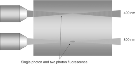
6.12 Two-photon fluorescence indicating the energy transfer from the laser to the material. The string confinement around the laser focus enables the high spatial resolution and the three-dimensional structuring.
Due to the unique properties of two-photon-absorption (TPA)-based 3D-LL, an increasing number of groups deal with 3D fabrication of polymer structures for various applications. Therefore, numerous comprehensive review papers can be found in the literature about the recent progress in multiphoton micro-fabrication with femtosecond lasers (Fourkas and Baldacchini, 2004; LaFratta et al., 2007; Maruo and Kawata, 1998), and direct laser-written 3D polymer templates for advanced nanostructures for photonics (von Freymann et al., 2010).
A related topic, which exploits the 3D features of the two-photon technology is 3D data storage. Taking advantage of 3D multilayer storage would enable capacities of 10 Tbyte on a DVD-size disk (Walker and Rentzepis, 2008). The recording of optical data realized by photodegradation of fluorescent chromophores at a spatial resolution of less than 1 μm in three dimensions has been successfully demonstrated by Nakahama et al. (2005).
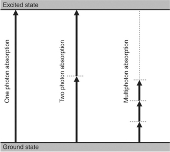
6.4.1 Two-photon absorption – team play of photons
Seventy years ago, Maria Göppert-Mayer discussed the fundamentals of two-photon absorption in her PhD thesis (Göppert-Mayer, 1931). However, the experimental proof was demonstrated three decades later in 1961 (Kaiser and Garrett, 1961). Phenomena including more than one photon (multiphoton absorption and multiphoton ionization) occur in materials at high intensities of the incident radiation. With the simultaneous presence of a large number of photons in the same place, it may happen that a photosensitive entity absorbs multiple photons with energies below the energetic gap between the ground and the excited state (Fig. 6.13). At high laser intensities, the absorption coefficient of a material becomes intensity dependent (Boyd, 2003), which leads to a modified Beer-Lambert absorption law and a nonlinear dependence of absorbed energy on the incident laser intensity. Thus, a localization of the energy transfer to the material around the laser focus takes place, even for radiation that is spectrally located in a transparent region of the photosensitive material. The nonlinear intensity dependence facilitates the high achievable spatial resolution and true three-dimensional structuring capability (Fig. 6.14). 3D-LL based on the simultaneous absorption of multiple (n > 1) photons was first proposed by Maruo et al. (1997) in photo-polymerizable resin. The resin is hardened by a polymerization process, which is triggered by two-photon absorption. Small 3D features with a lateral and axial (with respect to the laser beam) resolution of 0.62 μm and 2.2 μm are immediately fabricated by scanning the laser focus through the resin volume. The main limiting factor of the achievable resolution is attributed to spherical aberration at the resin–air interface (Maruo and Kawata, 1998). Hence, this method circumvents drawbacks of other rapid prototyping methods based on a sequential layer-by-layer approach, because the laser focus can be arbitrarily scanned in three dimensions through the volume of the photosensitive resin and more structure-related scanning strategies (including non-horizontal scanning approaches, cf. Section 6.4.3 and Section 6.6.1) can be developed. A short description of the method can be found in the literature (Gebeshuber et al., 2010).
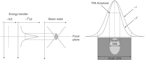
6.14 Nonlinear absorption enhances spatial resolution of TPA process as compared to SPA. The nonlinear energy transfer decreases faster in radial direction than a linear process and peaks at the focal plane of a Gaussian beam. Hence, the TPA process strongly confines energy transfer axially and radially to the voxel size. See also Maruo and Kawata (1998).
The underlying mechanisms of photo-polymerization including the rate of free electron generation via avalanche mechanisms and nonlinear absorption mechanisms at tight focusing conditions are considered important regarding chemical bond breaking, photo-initiation and structural material changes. The difference between high and low irradiance as well as the difference between high and low repetition regime is related to the material cooling mechanisms (Malinauskas et al., 2010b).
Multiphoton processes are technically exploited for spectroscopy, microscopy, and induced damage of various optical materials. Furthermore, laser-induced material modification by multiphoton absorption is of growing interest regarding 3D micro- and nano-fabrication, which is discussed later in this chapter.
The future development of micro- and nano-fabrication of micro- or nano-sized devices or devices with micro- and nano-features, which is an important task of nano-photonics, is expected to be essentially influenced by two-photon polymerization (TPP). TPP is an important method of multiphoton-based laser micro- and nano-fabrication and should play an important role in producing polymer-based optoelectronic and MEMS devices, since it offers fabrication of 3D structures below the diffraction limit (Witzgall et al., 1998). It is also expected that this method will penetrate many scientific research fields due to ongoing research in materials, optics and fabrication of functional devices. From the materials point of view, there is a need for highly efficient two-photon reactive materials, which will reduce costs for equipment, and a need for functional chromophores as a bonded component for advanced material with specially tailored properties. The optical point of view deals with adapting the voxel size and shape and a mechanism for a parallel production system, such as micro-lens arrays, which increase the number of foci (Sun and Kawata, 2004).
6.4.2 Technical implementation of 3D-LL based on TPA
There are some comprehensive reviews of two-photon-based micro-fabrication (e.g. Maruo and Fourkas, 2008; Sun and Kawata, 2004), which include also an overview of the development of laser lithography setups (Sun and Kawata, 2004). Basically, it is possible to provide the photons from two different laser beams in a ‘crossbeam’ arrangement. The advantages are the use of two different wavelengths (colors) and a better longitudinal resolution, but the alignment of such an optical system is difficult because the two beams have to overlap in space and time in the photosensitive sample (Sun and Kawata, 2004). Therefore, a setup similar to a laser scanning microscope is preferable. A single laser beam is tightly focused into the photosensitive resin and both photons are provided from the single laser beam. One advantage is the rather simple experimental setup although a two-color setup similar to the crossbeam setup with improved longitudinal resolution is not possible. There are other means (e.g. shaded ring filter [SRF], phase masks, beam shaping) to improve longitudinal/axial resolution for a single beam setup. Diffractive elements have also been introduced in the optical path, which decrease laterally the size of the point spread function of the focused laser beam in order to increase the resolution of the two-photon polymerization process (Wei et al., 2011). Another way of setting up multiphoton lithography is by raster scanning a focused fs laser beam over a digital mirror device (DMD) that represents a computer-controlled intrinsically aligned reflective photo mask. The reflection pattern from the DMD is imaged onto a photosensitive material by a high NA objective. A 2D pattern can be fabricated easily and a layer stacking of multiple patterns is fast and simple due to the inherent alignment of the DMD reflection patterns (automated mask sequence) and synchronized plane-to-plane movement of the laser voxel (Nielson et al., 2009).
A typical experimental or lab-scale setup of a 3D-LL fabrication system comprises generally a pulsed (fs, ps) laser source, part or sample handling and positioning, a beam delivery system, which consists of transmission optics, focusing optics, scanning systems or fiber delivery. Femtosecond laser pulses are popular material processing tools regarding two-photon-based lithography, although they are expensive. Femtosecond lasers provide high peak power at moderate pulse energy and average power, which is beneficial for reducing thermal damage to materials.
The high achievable resolution of the two-photon absorption-based lithographic process requires high resolution positioning of the sample or the laser focus. The implementation is either via high-precision linear stages, galvano-scanners, piezo stages or a combination of multiple positioning units. A common combination uses the long travel ranges of high-precision linear stages in order to handle large samples and a fast scanning of the laser focus with a galvano-scanner unit. A large structure can be realized by stitching of multiple smaller structures. Another combination takes advantage of the large scanning ranges of motorized stages with lower positioning accuracy that carry a high-precision piezo stage with a smaller scanning range but a much better positioning accuracy. For large-scale samples and applications that require a spatial resolution in the micrometer range, a sample motion with the motorized stages is done and stitching is not necessary. Photonic applications usually require high spatial resolution, which needs piezo stages for sample positioning.
Galvano-mirror scanning has a fast scanning speed, but suffers from a small fabrication area and distortions by the focusing lens. In contrast, piezo stage scanning is slower, but benefits from a larger fabrication area and better fabrication uniformity due to the absence of lens distortions (Yi and Kong, 2007).
The fabrication over large areas with piezo stages can be optimized by applying a continuous scanning method. This method takes advantage of the slow response of the piezo system at higher scanning speeds and is preferable to a point-to-point motion and a corresponding dwell time for exposure. A stable fabrication window with adequate stage settings enables uniform motion of the stage without errors considering the stage characteristics and hence provides optimized resolution and uniformly exposed material at minimized processing times (Lim et al., 2008).
With respect to a large format fabrication based on two-photon polymerization in suitable materials, the laser writing process must be optimized regarding the fabrication time. Laser power, repetition rate, sample scan speed and voxel size are not independent from each other and from the material. The optimal parameters must be determined from calibration experiments that screen different exposure (scan speed versus laser power) and determine the size of the inscribed voxels by scanning electron microscopy in order to account for a sufficient polymerization of the material at a given scan speed (Liu et al., 2010).
3D-LL for TPA is usually implemented with a titanium-sapphire (Ti:S) laser, which emits radiation in the near-infrared (NIR) range, typically 750–850 nm. These systems consist typically of a Ti:S oscillator or a frequency doubled fiber laser, that provide a pulse train at a repetition rate at several tens of MHz (80–100 MHz) and a pulse width of approximately 80–150 fs. Ti:S oscillators are often used to induce TPA in polymer materials since they provide enough power. In order to increase the variety of materials, an amplification stage can be implemented. This results typically in higher peak power of the provided laser pulses, but at a lower repetition rate in the kHz regime. Long cavity lasers provide pulses at higher power than oscillators at a reasonable fast repetition rate of typically 10–20 MHz. The Ti:S crystal as gain medium is well suited for the generation of fs pulses due to its wide spectral emission, but it is also reported that lasers with other active materials such as Yb:KGW (ytterbium doped potassium-gadolinium tung-state crystals) are used for two-photon polymerization in polymer materials (Malinauskas et al., 2010a). The second harmonic of such a laser is in the visible range, which is beneficial regarding the resolution limit of the method. A good spatial beam profile of the emitted TEM00 mode is essential for tight focusing of the laser. Fiber lasers offer a nearly perfect profile, which is generally better than from amplified Ti:S systems and better suited for the highest achievable resolution.
Although a 3D-LL apparatus can be built up in a modular way by combining the above-mentioned components, a compact setup is advantageous regarding the spatial resolution, stability, repeatability and quality of the 3D micro- and nanostructures. Today, there are systems available that are built on a microscope or inverted microscope (Fig. 6.15) taking advantage of a stable beam delivery, sample positioning and visual inspection or live monitoring of the fabrication process. Another advantage is the combined positioning of the sample with a motorized stage and a high-precision piezo stage. Additionally, different dimensions and scales of structures can be addressed by using different high NA (up to NA = 1.4 with oil immersion objectives) or low NA objectives. A system that is equipped with a motorized objective revolver enables automatic change of the fabrication resolution by simply changing the objective.

6.15 Typical writing setup fort two-photon-based 3D-LL. Reproduced with permission from Nanoscribe GmbH.
The increasing interest of industry and research pushes the number of commercially available lithographic systems for a routine fabrication of 3D micro- and nanostructures from several suppliers. The lithographic systems have outgrown the lab-only use and provide reliable tools for micro- and nano-rapid prototyping. Advanced systems offer a user-friendly control setup with automation of the writing process (remote control and programming, automatic sample exchange/handling) and CAD interface in combination with optimized optics for compensation of laser beam distortions (temporal as well as spatial pulse profile) and focusing. Optional optical features such as shaping of the voxel volume are available by means of filters (e.g. shaded ring filter), which change the point spread function of the beam and reduce the axial elongation of the voxel (Fig. 6.16), important for photonic applications or applications, where structuring close at the resolution limit is required (e.g. 3D meta-materials). Beside beam shaping of the laser focus by cylindrical telescopes (Cerullo et al., 2002), axicons (Winfield et al., 2007) and slits (Ams et al., 2005) a dual beam approach for voxel shaping and enhanced resolution is reported (Fischer et al., 2010).

6.16 Point spread function of focal volume. Lines of constant intensity show the shape and size of the focal volume without (lhs) and with (rhs) shaded ring filter (SRF). A reduction of >28% of the axial elongation is achieved. Reproduced by courtesy of Erik Waller and Georg von Freymann, TU Kaiserslautern.
The structuring process is optimized via various computer-controlled writing parameters such as the laser power, scan speed, distance between individual voxels, acceleration, deceleration of the positioning system and synchronized ramping of the laser power.
The offered flexibility facilitates the generation of 2D and 3D structures in photosensitive materials with high and low refractive index for photonic applications, whereas positive-tone and negative-tone materials are available for two-photon-based direct laser writing. Via polymer templates, 3D structures can be molded in materials that are not suitable for direct laser writing.
Recently, direct laser writing of three-dimensional submicron structures using a continuous wave (cw) laser at 532 nm was demonstrated (Thiel et al., 2010). Using such a laser at moderate powers (some 10 mW for commercially available photoresists such as SU-8 or IP-L and IP-G) significantly reduces the cost and increases the reliability and stability of advanced optical lithographic systems.
Recently, large-scale patterning based on two-photon absorption in inorganic–organic hybrid materials was realized (Houbertz et al., 2010). A setup similar to micro-stereolithography was applied. The setup is inverted, that is, the laser is focused from the bottom side into a material bath with an immersed sample holder. The structure is generated head over heels and structures with dimensions of several mm up to 2 cm at high spatial resolution were processed (Fig. 6.17).
6.17 Large-scale fabrication of 3D structures according to Houbertz et al. (2010).
6.4.3 Technical benefits of 3D-LL based on TPA
Applications that require a true 3D fabrication method for intricate structures at high resolution (sub-diffraction limit resolution) with great flexibility in design benefit from 3D-LL based on TPA. As a rapid prototyping method it facilitates the direct conversion from a CAD model to a physical structure with reliable and reproducible results in a single exposure step. True 3D offers the adaptation of the laser focus scanning strategy according to the geometry, that is, slicing, hatching and contouring of a 3D model is not restricted to planes parallel to the substrate (horizontal slices). Vertical and horizontal scanning are possible in the same way. Similarly, vertical and horizontal stitching can be made for the direct writing of large and tall structures over larger areas or volumes. The vertical limit is mainly given by the focal length of the objective. Therefore, 3D-LL is situated between high resolution processes such as electron beam lithography or focused ion beam lithography and processes with worse resolution such as micro-stereo-lithography. The simple apparatus without vacuum requirements facilitates a faster and higher throughput than, for example, e-beam lithography and hence has the potential for mass production. Upon availability of efficient material the costs of the equipment are further reduced due to the possibility to use cheaper laser systems for triggering the TPA process. The material development supports the trend to faster writing speeds and larger sample areas. Technical implementation of machine vision enables the processing of pre-configured substrates in order to align laser-inscribed structures into micro-systems. Depending on the optical configuration of the apparatus, both transparent and opaque substrates can be handled. For this purpose, 3D-LL is of growing interest in industry and research.
The above-mentioned benefits can be technically exploited to make superior micro- and nanostructures. There are several benefits of using two-photon absorption-based photo-polymerization rather than a one-photon-based polymerization: due to the localization of the laser–matter interaction around the laser focus, the polymerization is confined to a small volume inside the material volume (resin) and can be triggered within the bulk of the resin. Consequently, a 3D scanning of the laser focus across the resin yields a true 3D structure (no sequential layering) instead of a layer-by-layer processing initiated by a one-photon-based process. Additionally, the quenching of radicalized molecules and hence inhibited polymerization is avoided, since there is no direct contact with ambient oxygen inside the resin volume. Furthermore, two-photon absorption-based polymerization results in higher spatial resolution and smaller structure features as compared to one-photon absorption-based polymerization. The threshold of the two-photon absorption enables sub-diffraction limit feature sizes by controlling the laser power energy and the number of applied laser pulses per voxel. This yields very smooth surfaces as required by micro-optical components.
The achievable resolution of a structure depends on various parameters such as material chemistry, laser parameters (beam profile, pulse width) and writing parameters. An estimation of the achievable resolution is given by the investigation of the voxel size as a function of laser and writing parameters. The size and shape of the voxel can be studied by SEM characterization of the voxels. The shape of the voxel reveals additionally the internal structure of the focal volume of the laser, because it is sensitive to aberrations introduced by misalignment of the optical setup. The width of a voxel can be estimated from the intensity distribution from a focused Gaussian beam and the dependence of the squared intensity of the polymerization and easily measured by SEM characterization (Yi et al., 2005), but for the measurement of the vertical size of the voxel, an isolated voxel lying on the substrate is required. Since the voxel needs to be attached to the substrate in order to avoid being washed away during the development it is partly truncated and does not show its full shape. The ascending scan method circumvents this problem and avoids truncation of voxels and measurements on isolated voxels (Sun et al., 2002). The ascending scan method moves the laser focal position with respect to the substrate surface starting from inside the substrate. As the focus moves away from the interface, the voxel is less truncated and more weakly attached to the substrate. If the laser focus moves further, the voxel becomes detached and floats away during development. Some of the voxels that are barely attached will tilt over and exhibit the full longitudinal or axial elongation (Fourkas and Baldacchini, 2004; LaFratta et al., 2007). This method enables the voxel characterization (size and shape) as a function of exposure time and laser power and shows the influence of laser beam properties such as the polarization on the voxel formation or the numerical aperture of the focusing optics (Sun et al., 2003). The smaller a voxel gets, the more technically challenging is the application of the ascending scan method and the suspending bridge method can be used instead (Sun and Kawata, 2004). Instead of isolated voxels by single point/single pulse exposure, a suspended line is written between two posts, whereas the line width and height corresponds to the voxel dimensions. This method is also commonly used for determination of achievable resolution for various materials and systems.
In a polymerization process initiated by radicals, the voxel size can be estimated from a rate equation and the intensity distribution of a focused Gaussian beam (lateral and along the optical axis), assuming that polymerization starts when a certain threshold of generated radicals is exceeded upon incident laser pulses (Wu et al., 2006b).
Typical negative-tone photoresists have voxel with sub-diffraction diameters in the range 0.2–0.5 μm for a numerical aperture NA = 1.25 up to 2.4–4 μm for a NA = 0.25. The control over the laser power and the power of the focusing optics (numerical aperture) facilitates the generation of complex 3D structures at different length scales in the same structure (Malinauskas et al., 2010a). In addition to the numerical aperture of the focusing optics and the laser wavelength the laser pulse width shows an effect on the achievable fabrication resolution. A study of the voxel size as a function of the pulse width showed a decreasing voxel size with a stretched pulse length (up to picoseconds) (Kong et al., 2007).
Although usually laser wavelength in the NIR enables the realization of sub-diffraction-limit features in photo-polymers with high reproducibility, a laser wavelength in the VIS is preferable to an NIR wavelength regarding the achievable resolution (Malinauskas et al., 2010a; Thiel et al., 2010).
Nevertheless, it is possible to achieve a voxel size of approximately λ/50 with a 780 nm laser for a two-photon process by tuning the laser power and the scan speed. Additionally, repolymerization of the material leads to further reduction of the feature size of written lines down to just 15 nm (Tan et al., 2007).
The size of the voxel can be attributed to different interaction volumes, which are governed by different mechanisms and which are not known to the same extent. The smallest volume is determined by the threshold behavior of the two-photon process and depends on the minimum required photo-initiator concentration. All mechanisms contribute simultaneously to the achievable voxel shape and size. The technical interaction volume is determined by the hardware of the apparatus and can be optimized by using high NA optics, stabilization of the laser, and a high-precision positioning system, while the chemical interaction is influenced by material properties such as the reaction kinetics and the diffusion of initiator molecules and is more difficult to minimize (Houbertz et al., 2010).
6.5 Material modification aspects
Normally, ultraviolet (UV), visible (VIS) or infrared (IR) light is used to initiate photo-polymer reactions, but sources at a shorter wavelength or electron beam lithography have also been utilized. Since the development of the basic chemical and physical reactions of organic-based materials that are initiated by electromagnetic radiation, the related photo-polymer technology has been used in a wide variety of practical applications. The relation between photo-polymer chemistry and applications can be described by the exposure mode, the mechanism of the photo-polymer reaction and the visualization method, which is applied to detect changes that were induced by the exposure. The exposure mode differentiates between an imaging (patterned or ‘pattern-wise’) and non-imaging (e.g. flood) way of exposing the photo-polymer. An imaging exposure is a patterned exposure, which is either by optically projecting a mask onto the material or by scanning a focused light beam over the material for forming a well-defined pattern in the photo-polymer. A non-imaging exposure is, for example, a flood exposure of the photo-polymer or an exposure through a shadow mask without any optics. The mechanisms involved in photo-polymer reactions comprise photo-polymerization (crosslinking of monomers and oligomers to form higher molecular weight material), photo-crosslinking (reaction of unsaturated moieties, which are attached to an organic polymer), photomolecular reaction (reaction of small molecules, which modify the embedding polymer matrix), photodegradation (fragmentation of light sensitive linkages and degradation of the polymer into smaller units) and a photo-thermal reaction (physical changes such as laser ablation). All these reactions form detectable changes in organic materials, which can be visualized by an adequate visualization method. The light-induced changes are, for example, solubility, adhesion, color change, phase change, refractive index or electrical conductivity (Pfeiffer, 1997).
Upon exposure by light or laser, a latent image is formed in the photosensitive material, which must be developed. In most applications, the following different classes of visualization are used, which depend on the property change of the photo-polymer: if the solubility of the material is changed either by photo-polymerization or photo-crosslinking, which both transform an initially soluble material into an insoluble, or by photodegradation or photomolecular reaction, which both can make an insoluble material more soluble in an adequate solvent, the exposed material can be separated from the unexposed material and the latent image is made visible. In a similar way, other properties such as adhesion modulation, color changes, phase changes, changes of the refractive index or the electrical conductivity can be used to visualize the pattern in the photo-polymer (Pfeiffer, 1997).
In most of the described photonic applications in this chapter, the change in solubility and/or the refractive index is used for either the direct inscription of embedded photonic structures or the forming of a freestanding 2D or 3D shape after separation of exposed and unexposed material. Depending on the material system the polymerization happens during laser exposure via radically reacting photo-initiators (liquid resins such as acrylate-based systems or organically modified ceramics). Other materials such as SU-8 generate an acid and require a post-exposure baking in order to polymerize. Since the polymerization usually leads to a change of the refractive index, cationic systems such as SU-8, which have only a negligible change of refractive index upon laser exposure, allow a more flexible exposure strategy due to negligible perturbation of the laser focus due to index modulation (Ostendorf and Chichkov, 2006). The maintained transmittance and refractive index of the material is an important prerequisite for a true 3D scanning of the laser focus through the material and hence optimized exposure strategies for a time optimized fabrication of complex structures.
It was shown that 3D structures can be fabricated by using a thermo-sensitive resin in a micro-fabrication system. The nonlinear thermally triggered photo-polymerization shows similar capabilities for 3D fabrication such as the two-photon absorption-based lithography (Yamakawa et al., 2004).
6.5.1 Towards high efficient two-photon photo-initiators
An efficient photochemistry is a prerequisite for the application of a wide range of applications regarding two-photon-based laser lithography. An efficient photo-initiator in a suitable polymer matrix has a great impact on the fabrication result (Fig. 6.18). The development of efficient materials aims at improving the fabrication efficiency of 3D nano/micro-fabrications based on two-photon polymerization (TPP) and the development of organic molecules with large TPA cross-sections (Blanche et al., 2002).

6.18 (a) Result with a non-optimized photo-initiator; (b) result with an optimized photo-initiator. Exposure conditions are the same for both structures.
High TPA cross-sections are directly related to the molecule structure (Lee et al., 2008). Different donor-acceptor functionalities in cross-conjugated polymers allow investigation of the structure–activity relationship (Pucher et al., 2009). An efficient two-photon photo-initiator is technically very important, because it enables photochemistry far below the damage threshold of the material and therefore a wide power range for tailoring the micro-structure dimensions. In addition, the more efficiently a material can be structured, the less optical power is required for initiating the two-photon absorption process and hence the less expensive is the technical setup, since cheaper laser systems (cw or ns) instead of femtosecond laser systems can be used.
It was found that the spatial resolution in pinpoint photo-polymerization of radical-type resins is influenced by the temperature of the resin. A temperature decrease leads to a less pronounced radical diffusion, while a temperature increase leads to a voxel size reduction due to enhanced chain termination. In addition to the influence of the temperature on the polymerization effect, heated photonic structures showed a blue shift of the reflection spectra due to shrinking of the structure. Heating is considered to increase the robustness and facilitates a tuning of the working wavelength of photonic structures (Takada et al., 2008).
The development of photo-polymers for rapid prototyping is not restricted to optical systems, but is also of growing interest for biological applications. Structures can be made of newly developed acrylate-based biocompatible and biodegradable formulations for cellular implants with various rapid prototyping techniques such as digital light processing (DLP), micro-stereolithography (μ-SL) and rapid prototyping based on two-photon absorption photo-polymerization techniques. A new cross-conjugated photo-initiator for TPA was found recently, which enables micro-fabrication in biocompatible monomer formulation based on trimethylolpropanetriacrylate (TTA) at a very low photo-initiator concentration of 0.005 wt% (Liska et al., 2007). Epoxy/acrylate resins can be processed by two-photon-induced crosslinking of the acrylate groups and subsequent thermally linking the epoxy groups, without the need of directly writing into the epoxy system (Winfield and O’Brien, 2010).
The selective chemical functionalization of 3D polymer micro-structures was demonstrated and used for the fabrication of a functional micro-inductor (Farrer et al., 2006). Both acrylate and methacrylate monomers were used for 3D micro-fabrication in a sequential laser writing process. At increased laser power it was possible to create also methacrylic structures of similar quality as compared to acrylic structures. Due to the cross-reaction of methacrylates and acrylates it was possible to fabricate structures that are partially composed of acrylic and methacrylic polymer. Subsequent treatment added amines only to the acrylic portion of the structure, onto which other materials can be deposited. For example, a selective metallization can be achieved. This approach presents new possibilities for multiphoton-based micro-fabrication in areas such as photonic crystals, meta-materials or biosensing.
The good performance of 1,5-diphenylpenta-1,4-diyn-3-one (DPD) as photo-initiator for radical polymerization motivated the investigation of several donor substituted derivatives. Because of to the D-π-A-π-D system of these compounds two-photon-induced 3D photo-polymerization experiments were performed. It was found that the dimethylamino derivative N-DPD showed outstanding performance with respect to two-photon-induced photo-polymerization even at very low concentrations as compared to single-photon initiators such as Irgacure 369. Test structures were fabricated in a polymer matrix (1:1 blend of commercial trimethylolpropane triacrylate and ethoxylated trimethylolpropane triacrylate) that contains the N-DPD photo-initiator and compared to similar structures in the same polymer matrix but with the Irgacure 369 photo-initiator. Subsequent to fabrication, the structures were investigated by means of SEM. Taking into account the worse efficiency of Irgacure 369, a higher initiator concentration (approximately 1–1.5 wt%) and higher laser power was required for structuring. Nevertheless, no structures at sufficient quality could be processed in the material with Irgacure 369 in contrast to structures with very thin (300 nm) and smooth surfaces and high quality in the same matrix material with a lower concentration (0.025 wt%) of the very efficient photo-initiator N-DPD (Heller et al., 2007).
SU-8 is a commercially available, negative-tone photoresist for high aspect ratio micro-patterns in MEMS technology. It contains an epoxy resin and a photo-initiator, which are both dissolved in gamma-butyrolactone (GBL). A more detailed description of the composition and properties can be found in the literature (Teh et al., 2005). Upon irradiation by UV light, the photoinitiator generates a photoacid with a concentration that is proportional to the irradiation dose (latent image). A post-exposure bake is required for a chain reaction that converts the latent image into a crosslinking density. The degree of crosslinking determines the solubility in the developer. SU-8 was used for laser-based 3D micro-fabrication (Lim et al., 2008), fabrication of 3D photonic crystal templates (Hermatschweiler et al., 2007; Tétreault et al., 2006; von Freymann et al., 2010), biomimetics patterns (Lasagni et al., 2010), micro-fluidics (Liu et al., 2010), etc. The latent image has a negligible refractive index change and hence subsequent exposure steps do not influence each other (Deubel et al., 2004). SU-8 remains solid during the writing process. Since SU-8 is capable of forming thick films, up to mm height, high aspect ratio structures can be fabricated even with TPP. For this purpose, low numerical aperture focusing facilitates the exposure across the thick film and hence rapid processing at high lateral resolution. Structures with an aspect ratio up to 50 have been fabricated in SU-8 (Teh et al., 2005).
Organically modified ceramics (ORMOCER®s) are a class of inorganic-organic hybrid materials that have attracted attention in micro-optical (e.g. waveguides) and micro-electrical applications (e.g. dielectrics). They exhibit important properties such as low attenuation at standard telecom wavelengths (especially at 1310 and 1550 nm), a precisely tunable refractive index within a specific range (1.44–1.56 at 633 nm), surface planarization, no parasitic polymerization outside the exposed area and long-term stability (Houbertz et al., 2003). Such materials can be processed by mask aligner UV light exposure or by combining lithography, reflow and UV molding. Two-photon polymerization induced by 3D-LL based on TPA was used for the direct micro-fabrication from nm to mm scales with high precision and high optical quality (Houbertz, 2005). Organically modified ceramics are also used for the fabrication of movable complex 3D assemblies in one lithographic step using a UV laser. In order to reduce the penetration depth of the laser and to increase feature resolution, the material was mixed with azo phenyl UV absorbers (Overmeyer et al., 2011).
Acrylate-based transparent photo-polymers are suitable for micro-fabrication, whereas the photo-polymerization of the acrylate system transforms the reactive liquid into a solid polymer network. The polymerization is initiated by free radical species, which are generated upon two-photon absorption from a visible laser beam and well confined to the laser focus. Good adhesion, low shrinkage and a non-toxic removal of unexposed material are additional benefits (Nguyen et al., 2005).
The fabrication of 3D structures in a high-index material is accomplished either by the fabrication of a polymer templates with subsequent double-inversion or by high-index materials that can be directly patterned, such as chalcogenide glasses (Busch et al., 2007; Wong et al., 2006).
The full photonic bandgap of a 3D photonic structure requires high-index materials (refractive index n ~ 2–3) with a sufficient contrast to the ambient medium (generally air). TiO2 has a high refractive index (n ~ 2.4) and high transparency in the visible spectra and is therefore very promising for photonic applications. A direct 3D patterning with fs lasers is possible with a specially developed photosensitive sol–gel-based spin-coatable TiO2 resist, which has a refractive index of 1.68 and can be increased to > 2 by heating the film to temperatures between 400°C and 500°C due to a phase change of TiO2. The heating of fabricated TiO2 structures is challenging due to the strong shrinkage of the film, which results in deformation and delaminating of the structure from the substrate, although no fragmentation of the structure was observed (Passinger et al., 2007).
6.6 Device design, fabrication and applications
Usually 3D-LL machining systems use femtosecond lasers for the fabrication process. Such lasers offer sufficiently high pulse peak power for initiating a two-photon transition in the photosensitive material and moderate average energies, which avoids destruction of the surrounding material. A common system is a Ti:S laser system. The wavelength of such a laser is in the NIR (typically 750–850 nm) and is located in a transparent region of commonly used photosensitive materials.
In the past decades, many applications in the fields of electronic materials, printing materials, optical and electro-optical materials, fabrication of devices and materials, adhesives and sealants, coatings and surface modifications were generated (Pfeiffer, 1997).
Many manufacturing techniques have been developed and implemented to fabricate a wide range of micro-optical products. The challenges of the micro-optics business are diverse and tend to resist a widely accepted manufacturing process such as has been implemented for CMOS fabrication. Many of the challenges that have been addressed with various solutions include optical waveband of operation from DUV through LWIR, material systems, cost of manufacturing for the intended application space, feature sizes based on device functionality, and fabrication technology based on the manufacturing volume. Some of the technologies to be discussed include device patterning by e-beam lithography, optical lithography, gray-scale photolithography, direct CNC machining and micro-polishing, and plastic replication for applications such as micro-optics, micro-lenses, diffractive optics and refractive optics (Borek et al., 2007).
Infrared femtosecond laser pulses are ideal for the fabrication of 3D structures in transparent media. Due to the low absorption cross-section, two or more photons are necessary for absorption. This multiphoton effect limits the affected volume to the focal area allowing for sharp features on the order of the wavelength of light. One possible multiphoton reaction is the photo-destruction (ablation, decomposition, etc.) or photo-polymerization of materials. Using these techniques, 3D photonic components can be realized. A photonic bandgap template has been created with monodisperse polystyrene (PS) spheres (diameter ~ 624 nm). To optimally focus inside the bulk, an index matching material must be infiltrated. By using a photosensitive material, two-photon polymerization can be used to harden the material surrounding the spheres and insert defects inside the bulk. With proper placement of defects, 3D photonic components, that is, waveguides, splitters and filters, can be created (Boyle et al., 2007).
6.6.1 Optical design aspects
Nowadays, there are many versatile tools commercially available for design and simulation of optical components, as well as imaging or non-imaging systems. Pushed by the rapidly increasing computing power of desktop computers, optical modeling software became very powerful and can be used by everyone. The simulation tools are not restricted to simulate single optical components; the tools are capable of calculating the performance of a complete optical system with realistic material properties and a sufficient number of rays in a reasonable time for realistic predictions of system performance. In combination with optimization algorithms and tolerancing features, it is possible to design and create a virtual optical system that is already very close to the prototype, thus reducing costs drastically. Therefore, a close connection between simulations and rapid prototyping is considered crucial for photonic development. Once an optical design is made (including manufacturing tolerances and physical properties of the optical materials), normally a prototype of the designed optical system is required. Regarding microscale or nanoscale optics, 3D-LL is a very suitable method for rapid prototyping and designable nano-fabrication, which gives high resolution and the smoothest surfaces not only due to the small achievable voxel size but also due to the freedom in adjusting the voxel overlap and filling with liquid or partly polymerized resin with a surface tension-based self-smoothing effect (Zhang et al., 2010). Although there are many other laser-based rapid prototyping tools, none of them exhibits the required resolution. Usually, optical design programs support CAD data exchange, which can be used for transferring the CAD data into the lithographic apparatus.
There are manifold ray tracing tools for geometrical optics, tools for wave optics or tools for the design and optimization of photonic components such as diffractive optical elements, gratings, laser cavities, photonic crystals, waveguides, thin films, etc. These tools follow various mathematical approaches depending on their application focus. A main difference is the calculation of propagating rays (geometrical optics) or the calculation of propagating fields (wave optics). Some tools have hybrid algorithms and combine ray propagation with wave optics in order to account for coherent effects in macroscopic optical systems.
Optical simulations
The dimensions of optically relevant features in a photonic system determine the type of optical simulation that has to be performed for a system analysis or design. While ray tracing based on geometrical optics is well suited for the simulation of systems with dimensions larger than the wavelength such as illumination systems, imaging and non-imaging systems, it cannot be used for micro- and nano-photonics. Small-scaled features of photonic structures require a full vectorized solution to the Maxwell equations in order to cover all observed optical phenomena. Geometrical ray tracing requires fully featured non-sequential ray tracing, optimization algorithms and stray light analysis and is developed for the rapid development of refractive optics. Wave-optical effects including evanescent coupling, plasmonics and coherent superposition of polarized electromagnetic fields demand tools based on, for example. the beam propagation method (BPM) or the finite difference time domain (FDTD) algorithm. BPM cannot handle backwards propagating fields and therefore is not suited to account for reflections at system boundaries or refractive index mismatches. The FDTD algorithm is well established and is ideal for calculations of structured interfaces and refractive/diffractive systems with feature sizes in the order of the wavelength or even smaller. It calculates the decay of an injected electromagnetic pulse into the simulation region. It can be used for the design of gratings, coupling structures, color generating structures, dipole emission close to dielectric interfaces and nanoparticles, photonic bandgap structures, etc.
Modern simulation tools facilitate the CAD design of structures, include material databases and support the parameterization of systems for tolerance analysis and optimization. Subsequent to the system design, the simulation tool exports the structural data to a CAD compatible format that can be further processed by lithographic machining. Depending on the tool, post-processing of data is required.
While the design of microscopic refractive optical structures such as lenses is straightforward and can mostly be done by geometric ray tracing, the design of structures with sub-wavelength features is more demanding and usually incorporates different algorithms and approximations. Limitations imposed by fabrication should also be considered in the design phase, since the structure eventually needs to be realized (Mait et al., 1998).
Diffractive optical elements with a high efficiency require a multilevel representation of the designed phase structure (Fig. 6.19). A phase structure with 2N binary levels requires N separate masks, exposure and machining steps for its fabrication. For N = 4, the first machining (ion or laser etching) is done to a depth d/2N and d/2N−1 for the second machining step. Generally, the last etching step has to be done to half of the desired peak-to-peak depth of the structure (Goodman, 1996). Here, 3D-LL can be used to directly write a sawtooth structure without the need of multiple sequential processing (Fig. 6.20).
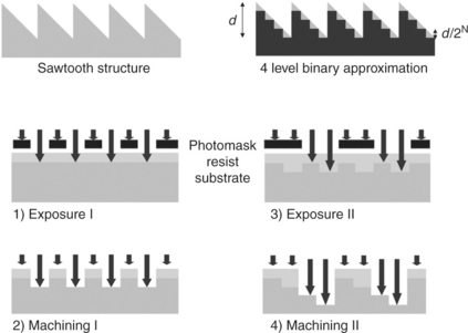
6.19 A diffractive sawtooth structure (a blazed grating element) and its 4-level binary equivalent. A mask-based lithographic fabrication process with a positive tone resist for 4 (N = 2, see text) height levels requires two masks with different patterns.

The optical design based on the representation of the electromagnetic field with all its properties such as spatial and temporal distribution, coherence, spectral distribution and polarization is essential for optical simulations that take into account effects that originate from the electromagnetic nature of light. An optical system is divided into its components and the light field is propagated through the system using appropriate propagation operators and assumptions. The optical design strongly relies on the right choice of the propagation operator and knowledge of its limitations in order to avoid numerical and physically non-existing artifacts. Today there are commercial software packages that facilitate the optical design without troubling too much about numerical issues and support the optical engineer with many tools for optimal design (Wyrowski and Schimmel, 2006, 2007).
Rapid prototyping aspects
Recent advances in multidimensional structures have been demonstrated that serve as the basis for three-dimensional photonic bandgap materials, meta-materials, optical cloaks, highly efficient low-cost solar cells, and chemical and biological sensors. The state-of-the-art design and fabrication of multidimensional architectures for functional optical devices are covered and the next steps for this important field are described in Arpin et al. (2010).
3D-LL can be easily integrated into a photonic structure development process. CAD data from an optical design are translated into a physical structure via 3D-LL rapid prototyping. By means of subsequent characterization an optimized prototype can be generated in an iterative way. Afterwards, large-scale replication of the component may start (Fig. 6.21).
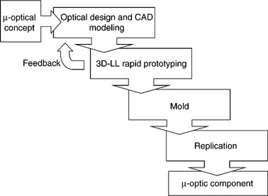
Beside the technical improvements of lithographic apparatus and the progress in material development, the writing strategy must be considered. Although the scanning of the laser focus in all three dimensions offers many ways of fabricating a structure directly from a CAD model, there are some ways that yield better results than others. The strategy of horizontally contouring is well suited for most shapes although other geometrical effects must be taken into account. Structures with many vertical lines can also be scanned vertically.
As a general rule, the voxel size correlates directly with applied scanning speed and numerical aperture of the focusing optics and correlates inversely with applied laser power (Zhou et al., 2008). This can be exploited for additional design features, because a very small distance between neighbouring voxels leads to a very even and smooth surface. A large distance may lead to the writing of separated, not connected voxels. With the right choice of voxel separation, a corrugated surface with a period smaller than the voxel diameter can be obtained (Woggon et al., 2009). Hence, the shape of the voxel gives additional freedom in structure design (cf. Fig. 6.22).

6.22 Influence of voxel size and separation on surface smoothness. At an appropriate separation between individual voxels, it is possible to write corrugated surfaces with a periodicity p smaller than the voxel diameter d. The same effect is achieved, when the largest part of the voxel is inside the substrate and structures such as lenses are written with only the topmost part of the voxel (diameter p).
Although the voxel diameter correlates to the achievable line width and resolution, post-processing of the fabricated structure such as O2 plasma ashing is used to decrease the line width of laser-written structures from 280 nm down to 60 nm (Park et al., 2006a).
Structural and shape enhancement methods
A simple representation of a structure by a (watertight) mesh requires additional hatching of the surfaces prior to the fabrication. If a freestanding structure is generated by exposure with subsequent removal of unexposed material (for the sake of simplicity a negative-tone photoresist is considered), the structure must be attached to the substrate in order to prevent floating and losing the structure during the development step.
The photochemistry and the change of optical properties of the photosensitive material must be considered. An immediate change of the refractive index may influence the laser beam by aberrations and focusing through already exposed regions can have a negative impact on resolution and voxel shape and may lead to unwanted results. Usually, the scanning of the laser focus is done in a defined way similar to the stacking known from stereo-lithography, either from the substrate or towards the substrate in planes parallel to the substrate surface (horizontal slicing). The thickness of each slice depends on the local slope of the structure and hence a uniform layer thickness may lead to a large number of slices. A small slope requires thinner slices, while steep slopes require fewer slices. For an efficient writing it is beneficial to divide a structure into subregions and each region is sliced with a layer thickness depending on the slope characteristics of each region. This subregional slicing reduces substantially the number of required slices and hence the fabrication time. The structural data of a shape can be obtained in different ways, according to the features of the designed model. Although the data represent the same shape, the fabricated structures may differ regarding the quality of the structure (Park et al., 2005).
Especially for larger structures it is advantageous to write only the shell of the structure, since exposing the whole volume would drastically increase the processing time. After removal of the unexposed material, the inner part of the structure may be UV cured by flood exposure, which solidifies the whole structure. A stress in the material may lead to fracture of the thin shell and the liquid resin inside the shell runs out, which leads to a destroyed structure. Writing at increased laser power leads to a larger voxel and hence reinforced shell but also to a reduced resolution. Therefore, multipath scanning is proposed for a shell reinforcement of the shell without losing spatial resolution and physical strength enhancement of the structure in order to avoid collapsing. In multipath scanning an offsetting contour to the original contour is obtained by translating the shell contour a distance towards its inside (Yang et al., 2007).
Among other rapid prototyping (RP) techniques that directly create a physical structure from a CAD model, 3D-LL shows a few unique benefits over other RP methods like micro-stereolithography or 3D printing. Due to the dependence of the energy transfer and hence the polymerization rate on the squared laser intensity, a much higher spatial resolution can be achieved. Since the structure is inscribed into the volume of the polymer material, there is no need for a layer-by-layer buildup of the 3D structure, hence there are nearly no geometrical limitations on the shape and the vertical (along the laser beam axis) resolution is not limited by the layer thickness of applied material as in stereolithography. Additional optics, which modify the transmitted laser beam profile, facilitate shaping of the focal volume of the laser beam in order to reduce the axial elongation of the beam even at weaker focusing with low numerical aperture objectives. It was shown that cylindrical telescopes (Cerullo et al., 2002), anamorphic beam shaping (Osellame et al., 2004) or a slit aperture (Ams et al., 2005) in the beam path are suitable to create a rather spherical volume instead of an elongated focal volume. This is especially important for the fabrication of symmetric multimode waveguides with a diameter of tens of microns (Schmidt et al., 2007a).
6.6.2 3D-LL based fabrication of photonic structures
3D-LL has proven to be suitable for the fabrication of diverse optical and photonic structures, which are presented in the following section. A clear advantage over other fabrication method is the true 3D writing, which facilitates the generation of monolithic optical components in a single exposure step and the three-dimensional integration of such structures in micro-systems with very small dimensions.
Optical waveguides
Nonlinear interaction between the tightly focused laser beam and the material enables the deposition of energy in hot plasma of free electrons leading to a permanent change of the refractive index due to structural material modifications. 3D-LL based on two-photon absorption has been used for direct inscription of waveguides in glasses (Osellame et al., 2004), in organic–inorganic hybrid materials (Schmidt et al., 2007a, 2007b), in a PDMS matrix (Infuehr et al., 2007) and modified porous silica films (Krivec et al., 2010). Additionally, direct laser writing is suited for repairing polymer waveguides in specially functionalized polymer materials that increase locally the refractive index upon laser heating. It enables the control over the power splitting ratio in waveguide branches via laser-induced change of the waveguide width at the splitter or fanout junction (Srisanit et al., 2005).
The possibility to change the refractive index of a material by exposure to intense laser pulses motivates the direct inscription of waveguides into transparent materials, whereas the change of the refractive index might be positive (increase of refractive index) or negative (decrease of refractive index), depending on the target material (Krol et al., 2004).
The illumination of semiconductor nanocrystal doped glasses with fs laser pulses induced a fairly high permanent change of the refractive index (1.8∙× 10−2) as compared to undoped glasses, which circumvents a usually observed drawback of directly written embedded photonic structures (Martinez-Vazquez et al., 2007).
It is possible to inscribe the waveguide in a longitudinal and in a transverse writing scheme (Fig. 6.23). In the longitudinal setup, the laser beam is focused in the material and the waveguide axis is orientated along the propagation axis of the laser beam. In contrast, in the transverse setup, the writing direction of the waveguide is perpendicular to the laser beam propagation axis. Although the longitudinal writing yields symmetric waveguides, the length of the waveguide is limited by the focal length of the focusing optic. Transverse writing is more flexible regarding the waveguide shape and the focal length of the optics limits only the inscription depth of the waveguide. Hence, transverse writing is the common technique to fabricate waveguides by means of laser fabrication. Unfortunately, without additional optical means, simple focusing of the laser beam in transverse writing suffers from the strong asymmetric shape of the focal volume in lateral and axial direction with respect to the beam propagation direction and hence very asymmetric waveguide cross-sections, which are disadvantageous for light coupling.
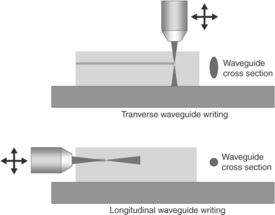
Introducing an asymmetry into the laser beam cross-section by astigmatically shaped beams (Osellame et al., 2004) or slit beam shaping (Ams et al., 2005) before focusing removes the asymmetry of the waveguide cross-section in the transverse writing scheme. This kind of beam shaping by a cylindrical telescope allows control of both cross-sectional shape and size of directly inscribed waveguides, because of control of the independent and individual beam waist in two orthogonal directions and the introduction of an astigmatic shift of the corresponding focal planes (Cerullo et al., 2002).
In contrast to the common concept of out-of-plane coupling of light into a planar waveguide based on a 90° deflection of the light via 45° mirrors or the use of immersed secondary emitters (fluorescent molecules) into waveguides (Steindorfer et al., 2010), 3D-LL facilitates the direct integration of photonic structures into printed circuit boards (PCBs) by means of in situ fabrication and alignment of optical interconnects (Fig. 6.24) (Langer and Riester, 2007). Such boards are capable of transmitting signals at a data rate of more than 7 Gbits/s at a bit error ratio of 10−9 (Schmid et al., 2009). Recently, PCBs with a more complicated optical interconnection system were fabricated that had two optical interconnects crossing each other at a distance of several tens of microns but did not intersect each other. A data rate of up to 8.25 Gbit/s at a bit error ratio of 10−9 was achieved. It was found that the data signal between the optical interconnects did not interfere and no optical cross-talk occurred. It was also shown that in contrast to an electrical signal line the optical data line was not disturbed by electrical noise that was added to the data signal (Langer et al., 2011).
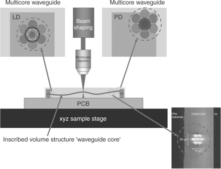
The waveguide alignment becomes an intrinsic part of the fabrication process. Provided that there is a suitable material that shows a sufficiently large refractive index change upon laser irradiation such as specially designed acrylate-based ORMOCER® (Houbertz et al., 2010), working optical interconnections were fabricated and integrated into an optical layer of a multilayer PCB (Schmidt et al., 2007a, 2007b). Optical interconnects exhibit a larger data transmission bandwidth and are robust against electrical noise. Their use is advantageous for high data rate applications, where a reliable connection even over long distances is required.
The fabrication of waveguides embedded in flexible matrix such as PDMS is based on selective photo-polymerization of monomers, which are swollen by photoreactive monomer formulations prior to the laser writing process. The reactive monomers contain acrylates or vinyl compounds with higher refractive index than PDMS. The monomer can be polymerized by two-photon absorption and the uncured monomer can be removed by evaporation at elevated temperatures leading to a local change of the refractive index (Satzinger et al., 2008).
The optical loss of a waveguide is a key parameter of the waveguide quality. Non-uniformity of the induced refractive index change may lead to increased optical losses of laser-fabricated waveguides. By splitting a single laser pulse into a pair of pulses at a delay in the femto- to picosecond range, the optical loss may be significantly reduced as compared to a single pulse exposure. This is due to a pre-conditioning of the optical material caused by a partial melting or softening of the material in the focal volume (Nagata et al., 2005).
Direct femtosecond laser-written waveguides were realized in freshly deposited thin chalcogenide glass films (Zoubir et al., 2004). The inscription happened at laser intensities below the ablation threshold and induced an increase of the refractive index at the waveguide location. Raman spectra revealed permanent structural change of the glass matrix due to modifications in the molecular arrangement of the film upon femtosecond laser irradiation.
A fast and cheap approach to waveguide fabrication is the laser-induced densification of Ti-doped SiO2 sol–gel films using a continuous wave Ytterbium fiber laser at 1070 nm and subsequent etching in order to remove unexposed material. Laser irradiated areas exhibit a lower etch rate. Due to internal stress, the laser power is limited to a certain fabrication window, whereas the laser power has influence on the width of the fabricated waveguides (Li et al., 2011).
Micro-optics
The fabrication of micro-optical features on non-planar surfaces facilitates novel hybrid optical elements. The challenging technical implementation requires the development of special laser lithographic equipment with auto-focusing and tilting options for substrate mount and beam delivery. The more complex scan motion and the mapping of the design data onto the curved substrate enables the fabrication of diffractive optical elements on top of biconvex lenses for imaging corrections (Radtke and Zeitner, 2007), or a micro-lens array on a concave lens, which can be combined with pinholes on a convex surface forming a spherical compound eye objective (Radtke et al., 2007).
In addition to directly inscribed waveguides, 3D-LL has been applied to the fabrication of polymer-based micro-lenses and micro-pyramids (Satzinger et al., 2008). Such structures represent optical features that can be directly integrated into a system or be replicated by imprint lithography via a PDMS mold. 3D-LL is capable of processing micro-optics on top of devices such as organic light emitting diodes or photo detectors for specially designed light coupling features and radiation characteristics. Femtosecond-based laser lithography is also capable of fabricating optical, fluidic, electronic and plasmonic elements in photosensitive glasses (Foturan). Even the fabrication of complex integrated systems with mirrors and a chamber containing a laser dye is reported (Cheng et al., 2008).
Micro-lenses in high-index GeO2–SiO2 glass films are fabricated by a combined process of laser writing and pattern transfer via plasma etching. For this purpose, a resist coats the glass film. The 3D shape of the lens is inscribed into the volume of the resist and subsequently transferred to the glass film with a CHF3 and O2 plasma treatment, yielding high-index glass lenses (Nishiyama et al., 2009). With the same approach it is possible to fabricate optical structures on non-planar inorganic substrates. It is demonstrated that a diffractive Fresnel lens can be processed on top of a refractive micro-lens. The combined process in yields a diffractive–refractive hybrid lens (Mizoshiri et al., 2009).
Gratings
Photonic structures such as gratings can be rapidly fabricated by laser interference lithography, where multiple laser beams are overlapped in a photosensitive material. The spatial intensity distribution of the interfering beams is translated into a physical structure of the photoresist. Upon removal of the unexposed material, a photonic relief structure is obtained. This method is well suited for the generation of large area defect-free periodic structures, but does not allow individual shaping of single grating lines. However, this is possible by direct laser writing of the lines, which facilitates ultimate freedom in designing the gratings and the fabrication of embedded gratings in semiconductor nanocrystal doped glasses (Martinez-Vazquez et al., 2007). Upon appropriate selection of the voxel overlap, structures with a periodicity smaller than the voxel diameter can be written, which was demonstrated with two-photon polymerization of ORMOCER® for the fabrication of a distributed feedback resonator with a grating period of 400 nm and a modulation depth of 40 nm for an optically pumped organic laser based on Alq3:DCM gain medium (Woggon et al., 2009). Additionally by changing voxel overlap and design, it is possible to combine gratings with different grating constants into a single hybrid grating structure, which could be used for color-separating purposes of transmitted light. Upon fs laser exposure (790 nm, 130 fs), embedded diffraction gratings in BK-7 glass are directly inscribed. The high peak intensity of the focused laser beam generates a plasma, which leads to a graded bulk index modification ranging from 2 × 10⁻³ up to 1.5 × 10⁻². The dimensions of the plasma formation are between 400 nm and 4 μm (Park et al., 2011).
The interference of fs laser pulses in a two-photon sensitive material is a hybrid structuring method that takes advantage of the periodic intensity modulation of laser interference lithography and the 3D features of two-photon-based 3D-LL. The optical arrangement requires the splitting of the laser beam and the introduction of a delay line for one laser pulse in order to control the spatial and temporal overlapping of the short pulses within the bulk material. The two-photon interaction between laser and material facilitates the inscription of a structure inside the bulk material and induces a local refractive index modulation. This yields embedded phase structures such as linear gratings without a surface relief (Guo et al., 2003). The interference of fs laser pulses shows a pulse width dependence of formed thin film surface relief Au–Cr gratings. Shorter pulse duration (25 fs) is preferable in terms of fabrication quality, since shorter pulses slightly above the ablation threshold exhibit smaller ablation fringes and hence higher spatial resolution (Wang et al., 2009).
Phase lenses and diffractive optical elements (DOEs)
Diffractive phase lenses with up to eight levels were fabricated by two-photon-based laser lithography (Chen et al., 2007). In contrast to Fresnel zone plates, which have alternating transparent and opaque zones, a phase lens is completely transparent. The alternating zones are defined either by different refractive index or step heights, which introduce the required phase shift for focusing transmitted light. Therefore, phase lenses offer usually a much higher efficiency than Fresnel zone plates. Depending on the number of levels the performance of phase lenses changes.
Alternatively to waveguides, DOEs have been designed and used for planar photonic devices and optical interchip interconnections of large-scale integration chips and proved to be suitable for a high degree of integration (Takamori et al., 2003).
The maskless approach of 3D-LL is ideally suited for the fabrication of DOE with binary levels or continuous grey-level encoding (256 phase levels) (Jia et al., 2007). From optical simulation, a phase transmission is generated that produces the desired intensity distribution in the image plane behind the DOE. From this data, a bitmap file, which represents the height profile pattern, is generated. The vectorized bitmap file data are used for controlling the sample motion of the apparatus (Fig. 6.25).

Fabrication of photonic crystals
A photonic crystal is the optical analogy to a crystal lattice, where atoms or molecules are periodically arranged and the periodic potential introduces gaps into the energy band structure of the crystal. Due to Bragg-like diffraction, electrons are forbidden to propagate with certain energies through the crystal and at a sufficiently strong potential the gap extends to all possible directions and a complete bandgap is built. In a photonic crystal, the periodic potential is replaced by the geometrical periodic arrangement of dielectric media. This leads to similar phenomena for photons in such a crystal as for electrons in a lattice. The optical phenomena are due to scattering at the periodic interfaces of the media that constitute the crystal. The optical properties of photonic crystal structures are influenced by the lattice period and structure and the effective refractive index, which is also modified by external agents. Thus, photonic crystals are used in various types of sensor applications, such as temperature sensors, humidity sensors, gas sensors, oil sensors, chemical sensors, biosensors, etc. A comprehensive overview of photonic crystal applications in sensorics is given in Nair and Vijaya (2010). Provided that the dielectric constants of the media differ sufficiently from each other and the absorption of the media is negligible, such a photonic crystal exhibits a photonic band structure that defines allowed and forbidden propagation states of photons within the volume of the crystal. A comprehensive treatment of photonic crystals can be found in Joannopoulos et al. (2008). Fabrication methods and applications of photonic crystals are presented in Thylén et al. (2004). It is evident that the influence of periodic dielectric media on light propagation enables an advanced use of light. Photonic crystal films, particles, fibers and photonic crystals in optofluidics facilitate novel applications not only in photonics, but also in bioassays (Zhao et al., 2010). Hence, suitable and powerful fabrication and replication methods are required. Photonic crystals could be beneficial for applications involving light emitting diodes and waveguides, where localization of light and modification of radiation behavior (Florescu et al., 2010) are required. A 3D photonic structure on a Si wafer, which is compatible with materials and standard micro-electronics fabrication methods, was realized more than 10 years ago (Lin et al., 1998). The 3D woodpile structure is made of polycrystalline Si and showed a transmission stop band in the infrared (10–14.5 μm) with a strong attenuation of light in this spectral region. Such a structure demonstrates the possibility to fabricate large-scale Si photonic crystals acting, for example, as filters in devices such as Si waveguides or photo detectors. Although the above-mentioned fabrication method is compatible with standard micro-electronics methods and takes advantage of the high refractive index of Si, it is a complex process to achieve the vertical topology of the 3D lattice structure. It is built by the repetitive deposition and etching of multiple dielectric films. For this reason, other methods for building complex 3D shapes were investigated. A rather straightforward approach to the fabrication of photonic crystals is direct inscription by ultrafast laser pulses (direct laser writing – DLW). Again, the benefits of a nonlinear interaction based on two- or multiphoton absorption between the laser and the dielectric material enables the direct 3D structuring of the material inside its volume. The 3D scanning of the laser focus through the bulk of the material and the associated modification of the material (photodegradation or photo-polymerization, etc.), which changes locally the refractive index and/or the solubility, create directly a photonic bandgap structure. Subsequent development removes either the exposed (positive-tone photoresist) or the unexposed (negative-tone photoresist) material. Important features of the lithographic method for the fabrication of photonic crystals are (a) good long-range periodic ordering; (b) intentionally engineered non-periodic defects; (c) high dielectric contrast; and (d) controllable feature size. DLW based on two-photon photo-polymerization has proved suitable for the fabrication of photonic crystal lattices with submicron features and arbitrary geometry (Kaneko et al., 2003). DLW is well suited for the fabrication of long-range periodic structures in photoresists (although the writing time may become an issue) and the introduction of structural defects in the periodic arrangement. Conventional photoresists with a refractive index around n = 1.5 suffer from low index contrast upon exposure and hence a complete bandgap is generally not achieved. Therefore, either higher-index organic, inorganic or hybrid materials are required that still can be structured by means of DLW. Other approaches such as atomic layer deposition or chemical vapor deposition use the DLW fabricated resist structures as 3D templates for transforming these structures into materials that are not suited for direct processing by DLW or structures that require a higher refractive index contrast than provided from the polymer structures. Alternative methods include inversion (Hermatschweiler et al., 2007) or double-inversion (Tétreault et al., 2006) of the templates with another high-index material such as Si. DLW written polymer templates are coated by a thin SiO2 film. After infiltration with silicon, etch of the SiO2 layer and calcination of the polymer, an inverse silicon structure is obtained. These advanced methods yield structures with a complete near-IR photonic bandgap or chiral polymeric photonic crystals, helical photonic crystals with polarization stop bands, and near-IR 3D photonic quasi-crystals. These types of structures and related fabrication methods are comprehensively reviewed in von Freymann et al. (2010).
Recently, metallic structures were fabricated from polymer templates by means of chemical-vapor deposition of Ag (Rill et al., 2008) or electroplated Au filling (Gansel et al., 2009).
Another approach towards the generation of metallic structures is the direct inscription of metallic structures in a polymer matrix, which is reported in Shukla et al. (2010). A two-photon-based in situ reduction of an Au salt and photo-polymerization of SU-8 produces gold nanoparticle doped polymer lines. The high loading of the film with the gold precursor yielded high quality metallic structures consisting of approximately 10 nm Au nanoparticles.
The direct fabrication of 3D, high-index-contrast woodpile nanostructures by DLW in chalcogenide glasses has shown a complete bandgap (Wong et al., 2006). The high index of the material required a partial compensation of optical aberrations for the writing in non-index-matched materials and a highly selective etchant for the accurate fabrication of the structure.
Another fabrication method of photonic crystals is based on the interference of multiple laser beams, also referred to as holographic fabrication. Multiple laser beams, which are aligned at certain angles of incidence, create a complex interference pattern, which exposes a photosensitive material. A comprehensive survey of nano-fabrication of photonic crystal structures can be found in the literature (Xia et al., 2010). Three-dimensional holographic patterning can be achieved also with a phase mask and a single laser beam. The phase mask creates multiple beams of a single incident beam that are phase locked to each other. Thus, the experimental setup is simpler as compared to a multiple beam setup and the sample quality is generally improved. Photonic woodpile structures with 3D periodicity were fabricated in a single beam 1D phase mask dual-exposure experiment, where the phase mask had been rotated and translated between the two exposure steps (Xu et al., 2010).
Furthermore, it is known that the introduction of controlled defects into photonic crystals is necessary in order to add functionality to the structures, which is comparable to that of dopants in semiconductors (cf. Braun et al., 2006).
Holographic lithography based on multiple beam interference can be combined with direct two-photon laser writing to produce photonic crystals containing precisely localized truly 3D structural modifications. This process has sufficient resolution to create embedded waveguide and micro-cavity structures by selectively modifying individual unit cells in the bulk of a 3D photonic crystal (Scrimgeour et al., 2006).
2D and 3D periodic structures with submicron features can be fabricated over large areas by interfering two laser beams with a wavelength in the absorption band of the photoresist, whereas the angle between the two beams facilitates the control over the periodic arrangement of the structure. 3D structures can be fabricated in a layer-by-layer approach, whereas different exposure conditions (line width of interference pattern, rotation of the sample for hexagonal patterns) for each layer facilitate a periodic but complex architecture (Lasagni et al., 2010).
Multiple beams for interference lithography can be generated by a conformal phase mask, which is fabricated by an imprinted phase-shift structure on top of a photoresist. This so-called proximity-field nanopatterning (PnP) takes advantage of diffraction from the phase mask and generates a 3D intensity distribution in the underlying photoresist. Advantages of PnP over interference lithography with multiple beam is the single beam exposure of a single self-aligned diffractive structure and reduced requirements on the coherence of the laser due to the proximity of the photoresist to the conformal mask. Hence, this method is also compatible with two-photon-based exposure of thick polymer films (Jeon et al., 2006). Two-photon-based exposure provides an increased range of 3D structure geometries and generates better images in the photoresist due to the squared intensity dependence of energy transfer from the laser to the material (George et al., 2009).
A review of PBG fabrication methods can be found in the literature (Lopez, 2003). Self-assembly for photonic structures has proven suitable (Galisteo-López et al., 2010). Pulsed fs laser irradiation resulted in self-organized formation of surface nano-gratings in soda-lime glass with a periodicity well below the laser wavelength, whereas the periodicity and orientation of the grating depended on the number of laser pulses and the laser polarization (Ahsan et al., 2011). However, self-assembly of colloidal nanoparticles may lead to unwanted defects such as missing particles or dislocations. Multiphoton polymerization can be used for direct pattern generation inside a 3D colloidal crystal (Lee et al., 2002; Pruzinsky and Braun, 2005). The pattern represents defect sites within the colloidal crystal. This method is considered less time consuming since the whole crystal does not need to be fabricated by multiphoton polymerization and the colloidal neighborhood stabilizes the inscribed defects.
Photonic crystals (PC) or photonic bandgap (PBG) structures can be processed in a wide range of materials by DLW (Deubel et al., 2004, 2006). They can be fabricated via optical damage in inorganic glasses, organic glasses, two-photon solidification in photo-curing resins with woodpile (Deubel et al., 2004) or spiral (Thiel et al., 2007) architectures. Another method is holographic lithography by multiple-beam interference for the generation of periodic light intensity patterns in 2D and 3D. Here, a photosensitive material is exposed to the interference pattern of multiple beams and subsequent silicon replication. In this context, shrinkage of the polymeric templates is found to be the most prominent deviation and requires pre-compensation (Meisel et al., 2006). Beside the low refractive index contrast, the deformation of photonic structures due to polymer shrinkage is considered mainly as contributing to the absence of a photonic bandgap in polymer structures. Hence a shape precompensation during the structure design is required and showed impact on the photonic bandgap for logpile structures (Sun et al., 2004) and photonic structure with a unit cell resembling the diamond lattice (Kaneko et al., 2003).
DLW facilitates the direct fabrication of 3D–2D–3D photonic crystal heterostructures (Deubel et al., 2006), which consist of a sandwiched 2D wave-guiding structure between a top and bottom cladding that is represented by a 3D PBG structure. The top and bottom PBG structure prevents optical out-of-plane losses of the 2D structure. DLW fabricates a polymeric template, which is replicated via silicon double inversion in order to get a corresponding high-index structure (Tétreault et al., 2006) with 3D square spiral architecture and a photonic stop gap centered at 2.5 μm (Seet et al., 2008).
Circular dichroism (different absorption for left and right circularly polarized light) is known from optically active chiral molecules and can be observed in dielectric chiral structures, which are, regarding losses, superior to metallic chiral structures. Similar to woodpile structures, layer-by-layer 3D chiral photonic crystals can be fabricated by DLW and work as thin film optical isolators (Thiel et al., 2007).
The threshold behavior of TPP can be exploited for structuring without the need of a shutter for the laser. At a given laser pulse energy the exposure dose and hence the effect of photo-polymerization can be controlled by the scan velocity of the laser focus with respect to the sample. First, the feature size can be controlled within the fabrication window of the material by adapting the scan velocity and sub-diffraction limited features can be fabricated. Second, above a certain velocity the exposure dose is insufficient to initiate photo-polymerization and discontinuous features can be written by simply changing the scan speed from below to above the threshold velocity (material and velocity dependent shutter mechanism) (Teh et al., 2004). This approach avoids the use of blocking the laser and simplifies a continuous scan strategy.
6.7 Conclusions and future trends
6.7.1 Conclusions
Since its invention in 1960, the laser proved its capability as a superior light source for scientific research and industrial applications. The laser provides a unique coverage of intensity (from highest power for laser fusion processes and material processing to lowest powers for laser therapy or optoelectronic components) and wavelength ranges (from deep UV to IR) due to the existence of manifold gain media, combined with properties such as long coherence length and polarization. Many modes of operation exist, from continuous wave to shortest pulses via Q-switching or mode-locking, and as a consequence of the manifold features of the laser there are manifold macroscopic and microscopic applications, such as applications in material science, photonics, μ-fluidics, medical applications, biotechnology, and as described in this chapter as a versatile lithographic tool.
The improvements in laser technology moved many applications from research labs into industrial and commercial applications. The laser proved compatible with established tools for optical lithography and pushed essentially optical lithography to lower and lower limits in terms of optical resolution. Laser interferometric lithography or a direct writing laser pen, combined with sophisticated scanning and masking methods, achieved 3D structuring, which is most important for the growing complexity of micro- and nano-systems. Owing to the achievable high intensity, nonlinear material aspects came into the focus of research and material development supported the establishment of laser writing methods based on the absorption of multiple photons. This method is also capable of fabricating 3D structures but without the use of masks and hence a rather simple optical setup. The three-dimensional nature is an intrinsic property of the laser writing process, which is accompanied by diffraction-unlimited spatial resolution. With increasing efficiency of photosensitive materials, the writing process is increasingly faster.
Nowadays, there are tools for 3D-LL for automated processing available that are equipped with many technical features such as auto-focus and automated tilt correction and work with transparent and opaque substrates. This technological maturity promises a bright future to direct laser writing methods and does not require preliminary steps for setting the laser focus location as reported in Park et al. (2006b). The realization of novel ideas with laser rapid prototyping is rather straightforward and simple with suitable laser tools. This holds true for nanoscale rapid prototyping, which is important for photonics. The promising combination of laser fabrication with other nano-processing widens the fields of applications and may set some future trends.
6.7.2 Future trends
Since DLW is a process that generates one structure after the other, highly efficient two-photon materials are a prerequisite for increasing the processing speed. Faster writing and parallel writing with multiple foci becomes possible and makes two-photon-based 3D-LL attractive to industrial or commercial applications. The combination with soft-lithography (PDMS molding) and the development of new materials that expand today’s available photosensitive materials is considered another step towards increasing technological exploitation of this tool.
Sophisticated optical setups applying more than one laser beam are about to be explored. A second annular shaped laser beam, which is used for photodepletion/deactivation is guided collinearly to the writing laser beam and increases the lateral resolution of the DLW process, where a λ/20 resolution is achieved (Li et al., 2009). NIR or visible light-based nano-lithography that reaches the same resolution targets (~ 30 nm) as compared to next generation lithography is very promising (Fourkas, 2010).
In order to increase writing speed and decrease the costs of the time consuming sequential writing process, micro-lens arrays can be used for parallel writing of identical structures. Provided that the laser delivers enough power, the laser beam can be expanded and focused on the sample with a micro-lens array (MLA). MLAs as big as 1 cm2 with micro-lenses at a period of 50 μm and a focal length in the μm range in order to produce numerous focused micro beams for parallel writing were used for the fabrication of phase masks (Huang et al., 2010). Such phase masks may be used in other lithographic methods: intricate polymer surface relief masks were fabricated by means of holographic lithography applying a phase mask. The structures were replicated by soft lithography and subsequently used as holographic elements for single laser beam exposure for the fabrication of 2D and 3D photonic elements (Goldenberg et al., 2010).
The direct laser printing of pixels useful for organic lighting or displays seems very interesting for future fabrication. The use of laser writing in a reel-to-reel tool would be a pathway to flexible and large-scale fabrication.
The increasing computational power of desktop PCs is advantageous for optical simulations and the more and more sophisticated technical implementation of laser lithography is a path towards optical systems of growing complexity, which makes light the most versatile means of material processing and information technology.
6.8 References
Ahsan, S., Md., Kim, Y.G., Lee, M.S. Formation mechanism of nanostructures in soda–lime glass using femtosecond laser. Journal of Non-Crystalline Solids. 2011; 357:851–857.
Ams, M., Marshall, G.D., Spence, D.J., Withford, M.J. Slit beam shaping method for femtosecond laser direct-write fabrication of symmetric waveguides in bulk glasses. Optics Express. 2005; 13(15):5676–5681.
Anscombe, N. Direct laser writing. Nature Photonics Technology Focus. 2010; 4:22–23.
Arpin, K.A., Mihi, A., Johnson, H.T., Baca, A.J., Rogers, J.A., Lewis, J.A., Braun, P.V. Multidimensional architectures for functional optical devices. Advanced Materials. 2010; 22:1084–1101.
Basting, D., Pippert, K., Stamm, U. History and future prospects of excimer laser technology. LPM2001: Focused on 2nd International Symposium on Laser Precision Microfabrication, May 16–18, 2001. RIKEN Review; 43. Data Storage Institute, National University of Singapore, Singapore, 2002.
Bäuerle, D.Laser: Grundlagen und Anwendungen in Photonik, Technik, Medizin und Kunst. Weinheim: Wiley-VCH Verlag, 2008.
Bettiol, A.A., Ansari, K., Sum, T.C., van Kan, J.A., Watt, F. Fabrication of micro-optical components in polymer using proton beam writing. Proceedings of SPIE. 2004; 5347:255–263.
Blanche, P.A., Kippelen, B., Schülzgen, A., Fuentes-Hernandez, C., Ramos-Ortiz, G., Wang, J.F., Hendrickx, E., Peyghambarian, N. Photorefractive polymers sensitized by two-photon absorption. Optics Letters. 2002; 27(1):19–21.
Borek, G., Weissbrodt, P., Schrenk, M., Cumme, M. Challenging micro-optical applications demand diverse manufacturing solutions. Proceedings of SPIE. 2007; 6462:1–11. [64620X].
Boyd, R.W. Nonlinear optics, 2nd. Burlington, MA: Academic Press, 2003.
Boyle, M., Neumeister, A., Kiyan, R., Reinhardt, C., Stute, U., Chichkov, B., Wohlleben, W., Leyrer, R.J. Production of 3D photonic components with ultrafast micromachining. Proceedings of SPIE. 2007; 6462:1–9. [646212].
Braun, A., Zimmer, K., Hösselbarth, B., Meinhardt, J., Bigl, F., Mehnert, R. Excimer laser micromachining and replication of 3D optical surfaces. Applied Surface Science. 1998; 127–129:911–914.
Braun, P.V., Rinne, S.A., García-Santamaría, F. Introducing defects in 3D photonic crystals: State of the art. Advanced Materials. 2006; 18:2665–2678.
Busch, K., von Freymann, G., Linden, S., Mingaleev, S.F., Tkeshelashvili, L., Wegener, M. Periodic nanostructures for photonics. Physics Reports. 2007; 444:101–202.
Byun, I., Kim, J. Cost-effective laser interference lithography using a 405 nm AllnGaN semiconductor laser. Journal of Micromechanics and Microengineering. 2010; 20:1–6.
Callegari, V. Fabrication of photonic elements by focused ion beam (FIB), 2009. [dissertation, ETH No. 18558, Zürich].
Cerullo, G., Osellame, R., Taccheo, S., Marangoni, M., Polli, D., Ramponi, R., Laporta, P., De Silvestri, S. Femtosecond micromachining of symmetric waveguides at 1.5 μm by astigmatic beam focusing. Optics Letters. 2002; 27(21):1938–1940.
Chen, Q.–D., Wu, D., Niu, L.–G., Wang, J., Lin, X.–F., Xia, H., Sun, H.–B. Phase lenses and mirrors created by laser micronanofabrication via two-photon photopolymerization. Applied Physics Letters. 2007; 91:171105.
Chen, Y.–P., Chiu, H.–C., Chen, G.–Y., Chiang, C.–H., Tseng, C.–T., Lee, C.–H., Wang, L.A. Fabrication and measurement of large-area sub-wavelength structures with broadband and wide-angle antireflection effect. Microelectronic Engineering. 2010; 87:1323–1327.
Cheng, Y., Xu, Z., Xu, J., Sugjioka, K., Midorikawa, K. Three-dimensional femtosecond laser integration in glasses. The Review of Laser Engineering. 2008; 36:1206–1209.
Chiu, C.-C., Lee, Y.-C. Fabrication of aspheric micro-lens array by excimer laser micromachining. Optics and Lasers in Engineering. 2011; 49:1232–1237.
Chong, T.C., Hong, M.H., Shi, L.P. Laser precision engineering: From microfabrication to nanoprocessing. Laser & Photonics Reviews. 2010; 4(1):123–143.
Cui, Z., Du, J., Guo, Y. Overview of greyscale photolithography for micro-optical elements fabrication. Proceedings of SPIE. 2003; 4984:111.
Daniel, C. Biomimetic structures for mechanical applications by interfering laser beams: More than solely holographic gratings. Journal of Materials Research. 2006; 21(8):2098–2105.
Debaes, C., Van Erps, J., Vervaeke, M., Volckaerts, B., Ottevaere, H., Gomez, V., Vynck, P., Desmet, L., Krajewski, R., Ishii, Y., Hermanne, A., Thienpont, H. Deep proton writing: A rapid prototyping polymer micro-fabrication tool for micro-optical modules. New Journal of Physics. 2006; 8:270–288.
Della Giustina, G., Zacco, G., Zanchetta, E., Gugliemi, M., Romanato, F., Brusatin, G. Interferential lithography of Bragg gratings on hybrid organic–inorganic sol–gel materials. Microelectronic Engineering. 2011; 88:1923–1926.
Desbiens, J.-P., Masson, P. ArF excimer laser micromachining of Pyrex, SiC and PZT for rapid prototyping of MEMS components. Sensors and Actuators A. 2007; 136:554–563.
Deubel, M., von Freymann, G., Wegener, M., Pereira, S., Busch, K., Soukoulis, C.M. Direct laser writing of three-dimensional hotonic-crystal templates for telecommunications. Nature Materials. 2004; 3:444–447.
Deubel, M., Wegener, M., Linden, S., von Freymann, G., John, S. 3D–2D–3D photonic crystal heterostructures fabricated by direct laser writing. Optics Letters. 2006; 31(6):805–807.
Dyer, P.E., Farley, R.J., Giedl, R., Karnakis, D.M. Excimer laser ablation of polymers and glasses for grating fabrication. Applied Surface Science. 1996; 96–98:537–549.
Elliott, D.J., Ferranti, D.C. Sub-micron lithography at 248 nm and 193 nm excimer laser wavelengths. Microelectronic Engineering. 1989; 9:59–63.
Ellman, M., Rodriguez, A., Pérez, N., Echeverria, M., Verevkin, Y.K., Peng, C.S., Berthou, T., Wang, Z., Olaizola, S.M., Ayerdi, I. High-power laser interference lithography process on photoresist: Effect of laser fluence and polarisation. Applied Surface Science. 2009; 255:5537–5541.
Ergin, T., Stenger, N., Brenner, P., Pendry, J.B., Wegener, M. Three-dimensional invisibility cloak at optical wavelengths. Science. 2010; 328:337–339.
Farrer, R.A., LaFratta, C.N., Li, L., Praino, J., Naughton, M.J., Saleh, B.E.A., Teich, M.C., Fourkas, J.T. Selective functionalization of 3-D polymer microstructures. Journal of the American Chemical Society. 2006; 128:1796–1797.
Farsari, M., Vamvakaki, M., Chichkov, B.N. Multiphoton polymerization of hybrid materials. Journal of Optics. 2010; 12:124001.
Fay, B. Advanced optical lithography development, from UV to EUV. Microelectronic Engineering. 2002; 61–62:11–24.
Fischer, J., von Freymann, G., Wegener, M. The materials challenge in diffraction-unlimited direct-laser-writing optical lithography. Advanced Materials. 2010; 22:3578–3582.
Florescu, M., Busch, K., Dowling, J.P. Thermal radiation in photonic crystals. Physical Review B. 2007; 75:201101R.
Flury, M., Benatmane, A., Gérard, P., Montgomery, P.C., Fontaine, J., Engel, T., Schunck, J.P., Fogarassy, E. Excimer laser ablation lithography applied to the fabrication of reflective diffractive optics. Applied Surface Science. 2003; 208–209:238–244.
Fourkas, J.T. Nanoscale photolithography with visible light. Physical Chemistry Letters. 2010; 1:1221–1227.
Fourkas, J.T., Baldacchini, T., Three-dimensional nanofabrication using multiphoton absorption. Dekker Encyclopedia of Nanoscience and Nanotechnology 2004;, doi: 10.1081/E-ENN 120021631.
Fritze, M., Tyrrell, B.M., Astolfi, D.K., Lambert, R.D., Yost, D.-R.W., Forte, A.R., Cann, S.G., Wheeler, B.D. Subwavelength optical lithography with phase-shift photomasks. Lincoln Laboratory Journal. 2003; 14(2):237–250.
Fu, Y., Ngoi, B.K.A. Investigation of diffractive-refractive microlens array fabricated by focused ion beam technology. Optical Engineering. 2001; 40:511–516.
Galisteo-López, J.F., Ibisate, M., Sapienza, R., Froufe-Pérez, L.S., Blanco, Á., López, C. Self-assembled photonic structures. Advanced Materials. 2010; 20:1–40.
Gansel, J.K., Thiel, M., Rill, M.S., Decker, M., Bade, K., Saile, V., von Freymann, G., Linden, S., Wegener, M. Gold helix photonic metamaterial as broadband circular polarizer. Science. 2009; 325:1513–1515.
Gattass, R.R., Mazur, E. Femtosecond laser micromachining in transparent materials. Nature Photonics. 2008; 2:219–225.
Gebeshuber, I.C., Belegratis, M., Schmidt, V. Emerging nanopatterning methods. In: Guston D., Golson J.G., eds. Encyclopedia of nanoscience and society. California: Sage Publications; 2010:184–185.
Geisler, S., Bauer, J., Haak, U., Stolarek, D., Schulz, K., Wolf, H., Meier, W., Trojahn, M., Matthus, E., Beyer, H., Old, G., Marschmeyer, S., Kuck, B. Double exposure technology for KrF lithography. EMLC 2008 – 24th European Mask and Lithography Conference. VDE VERLAG, Berlin Offenbach, 2008:62–70.
George, M.C., Nelson, E.C., Rogers, J.A., Braun, P.V. Direct fabrication of 3D periodic inorganic microstructures using conformal phase masks. Angewandte Chemie. 2009; 121:150–154.
Gläbe, R., Riemer, O. Diamond machining of micro-optical components and structures. Proceedings of SPIE. 7716, 2010. [771602-1].
Goldenberg, L.M., Gritsai, Y., Sakhno, O., Kulikovska, O., Stumpe, J. All-optical fabrication of 2D and 3D photonic structures using a single polymer phase mask. Journal of Optics. 2010; 12:1–7.
Goodman, J.W. Introduction to Fourier optics, 2nd. New York: McGraw-Hill, 1996.
Göppert-Mayer, M. Über Elementarakte mit zwei Quantensprüngen. Annalen der Physik. 1931; 401(3):273–294.
Guo, H., Jiang, H., Luo, L., Wu, C., Guo, H., Wang, X., Yang, H., Gong, Q., Wu, F., Wang, T., Shi, M. Two-photon polymerization of gratings by interference of a femtosecond laser pulse. Chemical Physics Letters. 2003; 374:381–384.
Guo, R., Xiao, S., Zhai, X., Li, J., Xia, A., Huang, W. Micro lens fabrication by means of femtosecond two photon photopolymerization. Optics Express. 2006; 14(2):810–816.
Guo, X.W., Dong, Q. Rapid fabrication of micro optical elements using DMD-based maskless lithography technique. Advanced in Materials Research. 2010; 146–147:143–146.
Heller, C., Pucher, N., Seidl, B., Kalinyaprak-Icten, K., Ullrich, G., Kuna, L., Satzinger, V., Schmidt, V., Lichtenegger, H.C., Stampfl, J., Liska, R. One- and two-photon activity of cross-conjugated photoinitiators with bathochromic shift. Journal of Polymer Science: Part A: Polymer Chemistry. 2007; 45:3280–3291.
Hermatschweiler, M., Ledermann, A., Ozin, G.A., Wegener, M., von Freymann, G. Fabrication of silicon inverse woodpile photonic crystals. Advanced Functional Materials. 2007; 17:2273–2277.
Hirai, Y., Inamoto, Y., Sugano, K., Tsuchiya, T., Tabata, O., Moving-mask UV lithography for 3-dimensional positive-and negative-tone thick photoresist microstructuring. Transducers. Solid-State Sensors, Actuators and Microsystems Conference, 2007, 2007:545–548, doi: 10.1109/SENSOR.2007.4300188.
Hon, K.K.B., Li, L., Hutchings, I.M. Direct writing technology – Advances and developments. CIRP Annals – Manufacturing Technology. 2008; 57:601–620.
Houbertz, R. Laser interaction in sol–gel based materials – 3-D lithography for photonic applications. Applied Surface Science. 2005; 247:504–512.
Houbertz, R., Domann, G., Cronauer, C., Schmitt, A., Martin, H., Park, J.-U., Fröhlich, L., Buestrich, R., Popall, M., Streppel, U., Dannberg, P., Wächter, C., Bräuer, A. Inorganic-organic hybrid materials for application in optical devices. Thin Solid Films. 2003; 442:194–200.
Houbertz, R., Steenhusen, S., Stichel, T., Sextl, G. Two-photon polymerization of inorganic-organic hybrid polymers as scalable technology using ultra-short laser pulses. In: Duarte F.J., ed. Coherence and Ultrashort Pulse Laser Emission. Rijeka, Croatia: Intech; 2010:583–608.
Huang, Z., Lin, Q.Y., Hong, M. Phase shift mask fabrication by laser microlens array lithography for periodic nanostructures patterning. JLMN – Journal of Laser Micro/Nanoengineering. 2010; 5(3):233–237.
Ihlemann, J., Rubahn, K. Excimer laser micro machining: Fabrication and applications of dielectric masks. Applied Surface Science. 2000; 154–155:587–592.
Infuehr, R., Pucher, N., Heller, C., Lichtenegger, H., Liska, R., Schmidt, V., Kuna, L., Haase, A., Stampfl, J. Functional polymers by two-photon 3D lithography. Applied Surface Science. 2007; 254:836–840.
Jahns, J., Cao, Q., Sinzinger, S. Micro- and nanooptics – An overview. Laser Photonics Review. 2008; 2(4):249–263.
Jang, H.S., Kim, G.H., Lee, J., Choi, K.B. Eliminating the undercut phenomenon in interference lithography for the fabrication of nano-imprint lithography stamp. Current Applied Physics. 2010; 10:1436–1441.
Jang, J.-H., Ullal, C.K., Maldovan, M., Gorishnyy, T., Kooi, S., Koh, C.Y., Thomas, E.L. 3D micro- and nanostructures via interference lithography. Advanced Functional Materials. 2007; 17:3027–3041.
Jeon, S., Malyarchuk, V., Rogers, J.A., Wiederrecht, G.P. Fabricating three dimensional nanostructures using two photon lithography in a single exposure step. Optics Express. 2006; 14(6):2300–2308.
Jia, B., Serbin, J., Kim, H., Lee, B., Li, J., Gu, M. Use of two-photon polymerization for continuous gray-level encoding of diffractive optical elements. Applied Physics Letters. 2007; 90:073503.
Joannopoulos, J.D., Johnson, S.G., Meade, R.D., Winn, J.N.Photonic crystals: Molding the flow of light. Princeton: Princeton University Press, 2008.
Kaiser, W., Garrett, C.G.B. Two-photon excitation in CaF2:Eu2+. Physical Review Letters. 1961; 7:229–231.
Kaneko, K., Sun, H.-B., Duan, X.-M., Kawata, S. Submicron diamond-lattice photonic crystals produced by two-photon laser nanofabrication. Applied Physics Letters. 2003; 83(11):2091–2093.
Kazansky, P.G., Qiu, J., Shimotsuma, Y., Bricchi, E., Hirao, K. Femtosecond laser nano-structuring of transparent materials. Proceedings of SPIE. 2004; 5399:88–95.
Kim, K.-R., Jeong, H.-W., Lee, K.-S., Yi, J., Yoo, J.-C., Cho, M.-W., Cho, S.-H., Choi, B. Rapid laser fabrication of microlens array using colorless liquid photopolymer for AMOLED devices. Optics Communications. 2011; 284:405–410.
Kim, S.H., Lee, K.-D., Kim, J.-Y., Kwon, M.-K., Park, S.-J. Fabrication of photonic crystal structures on light emitting diodes by nanoimprint lithography. Nanotechnology. 2007; 18:55306.
Kim, S.-K., Oh, H.-K., Jung, Y.-D., An, I. Advanced lithography simulation for various 3-dimensional nano/microstructuring fabrications in positive- and negative-tone photoresists. Journal of Nanoscience and Nanotechnology. 2011; 11:528–532.
Klein, F., Striebel, T., Fischer, J., Jiang, Z., Franz, C., von Freymann, G., Wegener, M., Bastmeyer, M. Elastic fully three-dimensional microstructure scaffolds for cell force measurements. Advanced Materials. 2010; 22:868–871.
Kondo, T., Yamasaki, K., Juodkazis, S., Matsuo, S., Mizeikis, V., Misawa, H. Three-dimensional microfabrication by femtosecond pulses in dielectrics. Thin Solid Films. 2004; 453–454:550–556.
Kong, H.J., Yi, S.W., Yang, D.-Y., Lee, K.-S., Kim, J.-B., Lim, T.-W., Kim, S. Pulse-width dependency of the fabricating resolution of the two-photon absorption photo-polymerization. Proceedings of SPIE. 6462, 2007. [646202-1].
Kordás, K., Pap, A.E., Lyöri, V., Uusimäki, A., Vähäkangas, J., Leppävuori, S. Mirror fabrication on optical fibres using maskless excimer laser-assisted methods. Surface and Coatings Technology. 2002; 155:285–288.
Krivec, S., Matsko, N., Satzinger, V., Pucher, N.U., Galler, N., Koch, T., Schmidt, V., Grogger, W., Liska, R., Lichtenegger, H. Silica-based, organically modified host material for waveguide structuring by two-photon-induced photopolymerization. Advanced Functional Materials. 2010; 20:1–9.
Krol, D.M., Chan, J.W., Huser, T.R., Risbud, S.H., Hayden, J.S. Fs laser fabrication of photonic structures in glass: The role of glass composition. Proceedings of SPIE. 2004; 5662:30–39.
Kunz, T., Stebani, J., Ihlemann, J., Wokaun, A. Photoablation andmicrostructuring of polyestercarbonates and their blends with a XeCl excimer laser. Applied Physics A. 1998; 67:347–352.
LaFratta, C.N., Baldacchini, T., Farrer, R.A., Fourkas, J.T., Teich, M.C., Saleh, B.E.A., Naughton, M.J. Replication of two-photon-polymerized structures with extremely high aspect ratios and large overhangs. Journal of Physical Chemistry B. 2004; 108:11256–11258.
LaFratta, C.N., Fourkas, J.T., Baldacchini, T., Farrer, R.A. Multiphoton fabrication. Angewandte Chemie International Edition. 2007; 46:6238–6258.
Langer, G., Riester, M. Two-photon absorption for the realization of optical waveguides on printed circuit boards. Proceedings of SPIE. 6475, 2007. [64750X-1].
Langer, G., Satzinger, V., Schmidt, V., Schmid, G., Leeb, W.R., PCB with fully integrated optical interconnects. Proceedings of SPIE 2011; 7944:794408, doi: 10.1117/12.873744.
Lasagni, A.F., Menéndez-Ormaza, B.S. Two- and three-dimensional micro- and sub-micrometer periodic structures using two-beam laser interference lithography. Advanced Engineering Materials. 2010; 12(1–2):54–60.
Lasagni, A.F., Hendricks, J.L., Shaw, C.M., Yuan, D., Martin, D.C., Das, S. Direct laser interference patterning of poly3, 4-ethylene dioxythiophene-polystyrene sulfonate (PEDOT:PSS) thin films. Applied Surface Science. 2009; 255:9186–9192.
Lasagni, A.F., Roch, T., Langheinrich, D., Bieda, M., Wetzig, A. Large area direct fabrication of periodic arrays using interference patterning. Physics Procedia. 2011; 12:214–220.
Lee, K.-S., Kim, R.H., Yang, D.-Y., Park, S.H. Advances in 3D nano/microfabrication using two-photon initiated polymerization. Progress in Polymer Science. 2008; 33:631–681.
Lee, S.-K., Park, H.S., Yi, G.-R., Moon, J.H., Yang, S.-M. Holographic fabrication of microstructures with internal nanopatterns using microprism arrays. Angewandte Chemie. 2009; 121:7134–7139.
Lee, W., Pruzinsky, S.A., Braun, P.V. Multi-photon polymerization of waveguide structures within three-dimensional photonic crystals. Advanced Materials. 2002; 14:271–274.
Li, A., Wang, Z., Liu, J., Zeng, X. Low cost fabrication of SiO2 optical waveguides by laser direct writing on Ti-doped sol–gel films. Optics and Lasers in Engineering. 2011; 49:351–355.
Li, L., Gattass, R.R., Gershgoren, E., Hwang, H., Fourkas, J.T. Achieving /20 resolution by one-color initiation and deactivation of polymerization. Science. 2009; 324:910–913.
Lim, T.W., Son, Y., Yang, D.-Y., Kong, H.-J., Lee, K.-S., Park, S.H. Highly effective three-dimensional large-scale microfabrication using a continuous scanning method. Applied Physics A. 2008; 92:541–545.
Lin, C., Wang, I., Bouriau, M., Casalegno, R., Andraud, C., Baldeck, P.L. Two-photon induced polymerization of photo-driven microsensors. Proceedings of SPIE. 2004; 5516:52–62.
Lin, S.Y., Fleming, J.G., Hetherington, D.L., Smith, B.K., Biswas, R., Ho, K.M., Sigalas, M.M., Zubrzycki, W., Kurtz, S.R., Bur, J. A three-dimensional photonic crystal operating at infrared wavelengths. Nature. 1998; 394:251–253.
Lippert, T., UV laser ablation of polymers: From structuring to thin film depositionMiotello A., Ossi P.M., eds. Laser–surface interactions for new materials production tailoring structure and properties. Springer Series in Material Chemistry; 130. Springer Verlag, Berlin, 2009:141–175.
Liska, R., Schuster, M., Inführ, R., Turecek, C., Fritscher, C., Seidl, B., Schmidt, V., Kuna, L., Haase, A., Varga, F., Lichtenegger, H., Stampfl, J. Photopolymers for rapid prototyping. Journal of Coatings Technology and Research. 2007; 4(4):505–510.
Liu, Y., Nolte, D.D., Pyrak-Nolte, L.J. Large-format fabrication by two-photon polymerization in SU-8. Applied Physics A. 2010; 100:181–191.
Logunov, S., Dickinson, J., Grzybowski, R., Harvey, D., Streltsov, A. Laser-induced swelling of transparent glasses. Applied Surface Science. 2011; 257:8883–8886.
Lopez, C. Materials aspects of photonic crystals. Advanced Materials. 2003; 15(20):1679–1704.
Lu, C., Zhou, J., Lipson, R.H., Ding, Z. Simple method to fabricate large scale quantum dot architectures. Materials Letters. 2009; 63:563–565.
Maiden, A., McWilliam, R., Purvis, A., Johnson, S., Williams, G.L., Seed, N.L., Ivey, P.A. Nonplanar photolithography with computer-generated holograms. Optics Letters. 2005; 30(11):1300–1302.
Mait, J.N., Prather, D.W., Mirotznik, M.S. Binary subwavelength diffractivelens design. Optics Letters. 1998; 23(17):1343–1345.
Makarovsky, O., Kumar, S., Rastelli, A., Patanè, A., Eaves, L., Balanov, A.G., Schmidt, O.G., Campion, R., Foxon, C.T. Direct laser writing of nanoscale light-emitting diodes. Advanced Materials. 2010; 22:3176–3180.
Malinauskas, M., Purlys, V., Rutkauskas, M., Gaidukeviciute, A., Gadonas, R. Femtosecond visible light induced two-photon photopolymerization for 3D micro/nanostructuring in photoresists and photopolymers. Lithuanian Journal of Physics. 2010; 50(2):201–207.
Malinauskas, M., Zukauskas, A., Bickauskaite, G., Gadonas, R., Juodkazis, S. Mechanisms of three-dimensional structuring of photo-polymers by tightly focussed femtosecond laser pulses. Optics Express. 2010; 18(10):10209–10221.
Marconi, M.C., Wachulak, P.W. Extreme ultraviolet lithography with table top lasers. Progress in Quantum Electronics. 2010; 34:173–190.
Martinez-Vazquez, R., Osellame, R., Cerullo, G., Ramponi, R., Svelto, O. Fabrication of photonic devices in nanostructured glasses by femtosecond laser pulses. Optics Express. 2007; 15(20):12628–12635.
Maruo, S., Fourkas, J.T. Recent progress in multiphoton microfabrication. Laser Photonics Review. 2008; 2(1–2):100–111.
Maruo, S., Kawata, S. Two-photon absorbed near-infrared photopolymerization for three-dimensional microfabrication. Journal of Microelectromechanical Systems. 1998; 7(4):411–415.
Maruo, S., Nakamura, O., Kawata, S. Three-dimensional microfabrication with two-photon-absorbed photopolymerization. Optic Letters. 1997; 22:132–134.
Meisel, D.C., Diem, M., Deubel, M., Pérez-Willard, F., Linden, S., Gerthsen, D., Busch, K., Wegener, M. Shrinkage precompensation of holographic three-dimensional photonic-crystal templates. Advanced Materials. 2006; 18:2964–2968.
Misawa H., Juodkazis S., eds. 3D laser microfabrication: Principles and applications. Weinheim: Wiley-VCH, 2006.
Mizoshiri, M., Nishiyama, H., Nishii, J., Hirata, Y., Silica-based microstructures on nonplanar substrates by femtosecond laser-induced nonlinear lithography. Journal of Physics: Conference Series 2009; 165:012048, doi: 10.1088/1742-6596/165/1/012048.
Mosher, L., Waits, C.M., Morgan, B., Ghodssi, R. Double-exposure grayscale photolithography. Journal of Microelectromechanical Systems. 2009; 18(2):308–315.
Murray, A.K., Dickinson, M.R. Tissue ablation-rate measurements with a long-pulsed, fibre-deliverable 308 nm excimer laser. Lasers in Medical Science. 2004; 19:127–138.
Mutapcic, E., Iovenitti, P., Hayes, J.P. A 3D-CAM system for quick prototyping and microfabrication using excimer laser micromachining. Microsystem Technologies. 2005; 12:128–136.
Nagata, T., Kamata, M., Obara, M. Optical waveguide fabrication with double pulse femtosecond lasers. Applied Physics Letters. 2005; 86:251103.
Nair, R.V., Vijaya, R. Photonic crystal sensors: An overview. Progress in Quantum Electronics. 2010; 34:89–134.
Nakahama, T., Yokoyama, S., Miki, H., Mashiko, S. Control of multiphoton process within diffraction limit space in polymer microstructures. Thin Solid Films. 2006; 499(1–2):406–409.
Neumeister, A., Himmelhuber, R., Materlik, C., Temme, T., Pape, F., Gatzen, H., Ostendorf, A. Properties of three-dimensional precision objects fabricated by using laser based micro stereo lithography. JLMN – Journal of Laser Micro/Nanoengineering. 2008; 3(2):67–72.
Nguyen, L.H., Straub, M., Gu, M. Acrylate-based photopolymer for two-photon microfabrication and photonic applications. Advanced Functional Materials. 2005; 15(2):209–216.
Nielson, R., Kaehr, B., Shear, J.B. Microreplication and design of biological architectures using dynamic-mask multiphoton lithography. Small. 2009; 5(1):120–125.
Nieto, D., Flores-Arias, M.T., O’Connor, G.M., Gomez-Reino, C. Laser direct-write technique for fabricating microlens arrays on soda-lime glass with a Nd:YVO4 laser. Applied Optics. 2010; 49:4979–4983.
Nishiyama, H., Nishii, J., Mizoshiri, M., Hirata, Y. Microlens arrays of high-refractive-index glass fabricated by femtosecond laser lithography. Applied Surface Science. 2009; 255:9750–9753.
Noh, J., Sohn, H., Suh, J., Shin, D., Lee, J. Fabrication of a rainbow color logo (diffraction grating) using the picosecond laser. Proceedings of the LPM 2007 – the 8th International Symposium on Laser Precision Microfabrication, April 24–28. University of Vienna, Vienna, Austria, 2007.
Okoshi, M., Iyono, M., Inoue, N., Yamashita, T. Photochemical welding of silica microspheres to silicone rubber by ArF excimer laser. Applied Surface Science. 2009; 255:9796–9799.
Osellame, R., Cerullo, G., Taccheo, S., Marangoni, M., Polli, D., Laporta, P., Ramponi, R. Femtosecond laser writing of symmetrical optical waveguides by astigmatically shaped beams. Proceedings of SPIE. 2004; 5451:360.
Ostendorf, A., Chichkov, B.N. Two-photon polymerization: A new approach to micromachining. Photonics Spectra. 2006; 40:72–79.
Othon, C.M., Laracuente, A., Ladouceur, H.D., Ringeisen, B.R. Sub-micron parallel laser direct-write. Applied Surface Science. 2008; 255:3407–3413.
Overmeyer, L., Neumeister, A., Kling, R. Direct precision manufacturing of three-dimensional components using organically modified ceramics. CIRP Annals – Manufacturing Technology. 2011; 60:267–270.
Ovsianikov, A., Chichkov, B., Mente, P., Monteiro-Riviere, N.A. Two photon polymerization of polymer-ceramic hybrid materials for transdermal drug delivery. International Journal of Applied Ceramic Technology. 2007; 4(1):22–29.
Ovsianikov, A., Ostendorf, A., Chichkov, B.N. Three-dimensional photofabrication with femtosecond lasers for applications in photonics and biomedicine. Applied Surface Science. 2007; 253:6599–6602.
Palla-Papavlu, A., Dinca, V., Luculescu, C., Shaw-Stewart, J., Nagel, M., Lippert, T., Dinescu, M. Laser induced forward transfer of soft materials. Journal of Optics. 2010; 12:124014.
Palla-Papavlu, A., Dinca, V., Paraico, I., Moldovan, A., Shaw-Stewart, J., Schneider, C.W., Kovacs, E., Lippert, T., Dinescu, M. Microfabrication of polystyrene microbead arrays by laser induced forward transfer. Journal of Applied Physics. 2010; 108:033111.
Papadopoulou, E.L., Axente, E., Magoulakis, E., Fotakis, C., Loukakos, P.A. Laser induced forward transfer of metal oxides using femtosecond double pulses. Applied Surface Science. 2010; 257:508–511.
Park, J.-K., Cho, S.-H., Kim, K.-H., Kang, M.-C. Optical diffraction gratings embedded in BK-7 glass by low-density plasma formation using femtosecond laser. Transactions of Nonferrous Metals Society of China. 2011; 21:165–169.
Park, S.H., Lee, S.H., Yang, D.-Y., Kong, H.J., Lee, K.-S. Subregional slicing method to increase three-dimensional nanofabrication efficiency in two-photon polymerization. Applied Physics Letters. 2005; 87:154108.
Park, S.-H., Lim, T.-W., Yang, D.-Y., Jeong, J.-H., Kim, K.-D., Lee, K.-S., Kong, H.-J. Effective fabrication of three-dimensional nano/microstructures in a single step using multilayered stamp. Applied Physics Letters. 2006; 88:203105.
Park, S.-H., Lim, T.-W., Yang, D.-Y., Kong, H.-J., Kim, J.-Y., Lee, K.-S. Direct laser patterning on opaque substrate in two-photon polymerization. Macromolecular Research. 2006; 14(2):245–250.
Partel, S., Zoppel, S., Hudek, P., Bich, A., Vogler, U., Hornung, M., Voelkel, R. Contact and proximity lithography using 193 nm Excimer laser in Mask Aligner. Microelectronic Engineering. 2010; 87:936–939.
Passinger, S., Saifullah, M.S.M., Reinhardt, C., Subramanian, K.R.V., Chichkov, B.N., Welland, M.E. Direct 3D patterning of TiO2 using femtosecond laser pulses. Advanced Materials. 2007; 19:1218–1221.
Pätzel, R., Bragin, I., Kleinschmidt, J., Rebhan, U., Basting, D. Excimer laser with high repetition rate for DUV lithography. Microelectronic Engineering. 1996; 30:165–167.
Pfeiffer, R.W., Application of photopolymerization technologyScranton A.B., Bowman C.N., Pheiffer R.W., eds. Photopolymerization: Fundamentals and Application. American Chemical Society: Washington, DC, 1997 Chapter 1
Photonics21. Lighting the Way Ahead: Photonics21 Strategic Research Agenda, 2nd. Düsseldorf: European Technology Platform Photonics21, 2010.
Pruzinsky, S.A., Braun, P.V. Fabrication and characterization of two-photon polymerized features in colloidal crystals. Advanced Functional Materials. 2005; 15:1995–2004.
Pucher, N.U., Rosspeintner, A., Satzinger, V., Schmidt, V., Gescheidt, G., Stampfl, J., Liska, R. Structure-activity relationship in D-TT-A-TT-D-based photoinitiators for the two-photon-induced photopolymerization process. Macromolecules. 2009; 42:6519–6528.
Radtke, D., Zeitner, U.D. Laser-lithography on non-planar surfaces. Optics Express. 2007; 15(3):1167–1174.
Radtke, D., Duparré, J., Zeitner, U.D., Tünnermann, A. Laser lithographic fabrication and characterization of a spherical artificial compound eye. Optics Express. 2007; 15(6):3067–3077.
Rapp, L., Nénon, S., Alloncle, A.P., Videlot-Ackermann, C., Fages, F., Delaporte, P. Multilayer laser printing for organic thin film transistors. Applied Surface Science. 2011; 257:5152–5155.
Reimer, K., Quenzer, H.J., Jürss, M., Wagner, B. Micro-optic fabrication using one-level gray-tone lithography. Proceedings of SPIE. 1997; 3008:279–288.
Rhee, H.-G. Direct laser lithography and its applications. In: Wang M., ed. Lithography. Rijeka, Croatia: InTech; 2010:1–16.
Richter, J., Meinertz, J., Ihlemann, J. Patterned laser annealing of silicon oxide films. Applied Physics A. 2011; 104:759–764.
Rill, M.S., Plet, C., Thiel, M., Staude, I., von Freymann, G., Linden, S., Wegener, M. Photonic metamaterials by direct laser writing and silver chemical vapor deposition. Nature Materials. 2008; 7:543–546.
Rodriguez, A., Echeverría, M., Ellman, M., Perez, N., Verevkin, Y.K., Peng, C.S., Berthou, T., Wang, Z., Ayerdi, I., Savall, J., Olaizola, S.M. Laser interference lithography for nanoscale structuring of materials: From laboratory to industry. Microelectronic Engineering. 2009; 86:937–940.
Rothschild, M. A roadmap for optical lithography. OPN Optics & Photonics News. 2010; 21:26–31.
Satzinger, V., Schmidt, V., Kuna, L., Palfinger, C., Inführ, R., Liska, R., Krenn, J.R. Rapid prototyping of micro-optics on organic light emitting diodes and organic photo cells by means of two-photon 3D lithography and nano-imprint lithography. Proceedings of SPIE. 6992, 2008. [699217-1].
Schmid, G., Leeb, W.R., Langer, G., Schmidt, V., Houbertz, R. Gbit/s transmission via two-photon-absorption-inscribed optical waveguides on printed circuit boards. Electronics Letters. 2009; 45(4):219–221.
Schmidt, V., Kuna, L., Satzinger, V., Houbertz, R., Jakopic, G., Leising, G. Application of two-photon 3D lithography for the fabrication of embedded ORMOCER® waveguides. Proceedings of SPIE. 6476, 2007. [64760P-1].
Schmidt, V., Kuna, L., Satzinger, V., Jakopic, G., Leising, G. Two-photon 3D lithography: A versatile fabrication method for complex 3D shapes and optical interconnects within the scope of innovative industrial applications. JLMN – Journal of Laser Micro/Nanoengineering. 2007; 2(3):170–177.
Schneider, C.W., Lippert, T., Laser ablation and thin film depositionSchaaf P., ed. Laser Processing of Materials. Springer Series in Material Science; 139. Springer Verlag, Berlin, 2010:89–112.
Scrimgeour, J., Sharp, D.N., Blanford, C.F., Roche, O.M., Denning, R.G., Turberfield, A.J. Three-dimensional optical lithography for photonic microstructures. Advanced Materials. 2006; 18:1557–1560.
Seet, K.K., Mizeikis, V., Kannari, K., Juodkazis, S., Misawa, H., Tétreault, N., John, S. Templating and replication of spiral photonic crystals for silicon photonics. IEEE Journal of Selected Topics in Quantum Electronics. 2008; 14(4):1064–1073.
Serbin, J., Gu, M. Superprism phenomena in waveguide-coupled woodpile structures fabricated by two-photon polymerization. Optics Express. 2006; 14:3563–3568.
Serbin, J., Ovsianikov, A., Chichkov, B. Fabrication of woodpile structures by two-photon polymerization and investigation of their optical properties. Optics Express. 2004; 12(21):5221–5228.
Shaw Stewart, J., Lippert, T., Nagel, M., Nüesch, F., Wokaun, A.Phipps C.R., ed. Laser-induced forward transfer using triazene polymer dynamic releaser layer. AIP Conference Proceedings 1278 – International Symposium on High Power Laser Ablation 2010. American Institute of Physics, New York, 2010:789–799.
Shaw Stewart, J., Lippert, T., Nagel, M., Nüesch, F., Wokaun, A. Laser-induced forward transfer of polymer light-emitting diode pixels with increased charge injection. ACS Applied Material Interfaces. 2011; 3:309–316.
Shin, D.S., Lee, J.H., Suh, J., Kim, T.H. Correction of a coherent image during KrF excimer laser ablation using a mask projection. Optics and Lasers in Engineering. 2006; 44:615–622.
Shukla, S., Furlani, E.P., Vidal, X., Swihart, M.T., Prasad, P.N. Two-photon lithography of sub-wavelength metallic structures in a polymer matrix. Advanced Materials. 2010; 22:3695–3699.
Srisanit, N., Liu, Z., Ke, X., Wang, M.R. Laser writing correction of polymer waveguide fanouts. Optics Communications. 2005; 244:171–179.
Stampfl, J., Baudis, S., Heller, C., Liska, R., Neumeister, A., Kling, R., Ostendorf, A., Spitzbart, M. Photopolymers with tunable mechanical properties processed by laser-based high-resolution stereolithography. Journal of Micromechanics and Microengineering. 2008; 18:125014.
Stampfl, J., Inführ, R., Stadlmann, K., Pucher, N., Schmidt, V., Liska, R. Materials for the fabrication of optical waveguides with two photon photopolymerization. Proceedings of the Fifth International WLT Conference on Lasers in Manufacturing, Munich, June 2009, 2009.
Stankevicius, E., Malinauskas, M., Raciukaitis, G. Fabrication of scaffolds and micro-lenses array in a negative photopolymer SZ2080 by multi-photon polymerization and four-femtosecond-beam interference. Physics Procedia. 2011; 12:82–88.
Steindorfer, M.A., Lamprecht, B., Schmidt, V., Abel, T., Mayr, T., Krenn, J.R. Light coupling for integrated optical waveguide-based sensors. Proceedings of SPIE. 7726, 2010. [77261S-1].
Steingrüber, R., Ferstl, M., Pilz, W. Micro-optical elements fabricated by electron-beam lithography and dry etching technique using top conductive coatings. Microelectronic Engineering. 2001; 57–58:285–289.
Stratakis, E., Ranella, A., Farsari, M., Fotakis, C. Laser-based micro/nanoengineering for biological applications. Progress in Quantum Electronics. 2009; 33:127–163.
Sum, T.C., Bettiol, A.A., Venugopal Rao, S., van Kan, J.A., Ramam, A., Watt, F. Proton beam writing of passive polymer optical waveguides. Proceedings of SPIE. 2004; 5347:160.
Sun, H.-B., Kawata, S. Two-photon photopolymerization and 3D lithographic microfabrication. APS. 2004; 170:169–273.
Sun, H.-B., Kawakami, T., Xu, Y., Ye, J.-Y., Matuso, S., Misawa, H., Miwa, M., Kaneko, R. Real three-dimensional microstructures fabricated by photopolymerization of resins through two-photon absorption. Optics Letters. 2000; 25(15):1110–1112.
Sun, H.-B., Maeda, M., Takada, K., Chon, J.W.M., Gu, M., Kawata, S. Experimental investigation of single voxels for laser nanofabrication via two-photon photopolymerization. Applied Physics Letters. 2003; 83(5):819–821.
Sun, H.-B., Suwa, T., Takada, K., Zaccaria, R.P., Kim, M.-S., Lee, K.-S., Kawata, S. Shape precompensation in two-photon laser nanowriting of photonic lattices. Applied Physics Letters. 2004; 85(17):3708–3710.
Sun, H.-B., Tanaka, T., Kawata, S. Three-dimensional focal spots related to two-photon excitation. Applied Physics Letters. 2002; 80(20):3673–3675.
Takada, K., Kaneko, K., Li, Y.-D., Kawata, S., Chen, Q.-D., Sun, H.-B. Temperature effects on pinpoint photopolymerization and polymerized micronanostructures. Applied Physics Letters. 2008; 92:041902.
Takamori, T., Wada, H., Sasaki, H., Kamijoh, T. Interchip optical interconnection using planar-type photonic circuit and optoelectronic integrated devices. Electronics and Communications in Japan. 2003; 86(1):9–17. [Part 2].
Tan, D., Li, Y., Qi, F., Yang, H., Gong, Q., Dong, X., Duan, X. Reduction in feature size of two-photon polymerization using SCR500. Applied Physics Letters. 2007; 90:071106.
Teh, W.H., Dürig, U., Drechsler, U., Smith, C.G., Güntherodt, H.-J. Effect of low numerical-aperture femtosecond two-photon absorption on SU-8 resist for ultrahigh-aspect-ratio microstereolithography. Journal of Applied Physics. 2005; 97:054907.
Teh, W.H., Dürig, U., Salis, G., Harbers, R., Drechsler, U., Mahrt, R.F., Smith, C.G., Güntherodt, H.-J. SU-8 for real three-dimensional subdiffraction-limit two-photon microfabrication. Applied Physics Letters. 2004; 84(20):4095–4097.
Tétreault, N., von Freymann, G., Deubel, M., Hermatschweiler, M., Pérez-Willard, F., John, S., Wegener, M., Ozin, G.A. New route to three-dimensional photonic bandgap materials:silicon double inversion of polymer templates. Advanced Materials. 2006; 18:457–460.
Thiel, M., Fischer, J., von Freymann, G., Wegener, M. Direct laser writing of three-dimensional submicron structures using a continuous-wave laser at 532 nm. Applied Physics Letters. 2010; 97:221102.
Thiel, M., von Freymann, G., Wegener, M. Layer-by-layer three-dimensional chiral photonic crystals. Optics Letters. 2007; 32(17):2547–2549.
Thylén, L., Qiu, M., Anand, S. Photonic crystals – A step towards integrated circuits for photonics. ChemPhysChem. 2004; 5:1268–1283.
Ting, C.-J., Chen, C.-F., Chou, C.P. Subwavelength structures for broadband antireflection application. Optics Communications. 2009; 282:434–438.
Torgersen, J., Baudrimont, A., Pucher, N., Stadlmann, K., Cicha, K., Heller, C., Liska, R., Stampfl, J. In vivo writing using two-photon-polymerization. Proceedings of LPM2010 – The 11th International Symposium on Laser Precision Microfabrication, June 7–10, 2010, Stuttgart, Germany, 2010.
Van Erps, J., Vervaeke, M., Debaes, C., Ottevaere, H., Van Overmeire, S., Hermanne, A., Thienpont, H. Deep proton writing: A powerful rapid prototyping technology for various micro-optical components. Proceedings of SPIE. 7716, 2010. [77160W-1].
Veiko, V.P., Kostyuk, G.K., Meshkovskii, I.K., Chuiko, V.A., Yakovlev, E.B. Microoptic components formed by local modification of the structure of porous glasses. Soviet Journal of Quantum Electronics. 1986; 16:8.
Voelkel, R., Vogler, U., Bich, A., Pernet, P., Weible, K.J., Hornung, M., Zoberbier, R., Cullmann, E., Stuerzebecher, L., Harzendorf, T., Zeitner, U.D. Advanced mask aligner lithography: New illumination system. Optics Express. 2010; 18(20):20968–20978.
von Freymann, G., Ledermann, A., Thiel, M., Staude, I., Essig, S., Busch, K., Wegener, M. Three-dimensional nanostructures for photonics. Advanced Functional Materials. 2010; 20:1038–1052.
Vossmerbaeumer, U. Application principles of excimer lasers in ophthalmology. Medical Laser Application. 2010; 25:250–257.
Walker, E., Rentzepis, P.M. Two-photon technology: A new dimension. Nature Photonics. 2008; 2:406–408.
Wang, J., Auyeung, R.C.Y., Kim, H., Charipar, N.A., Piqué, A. Three-dimensional printing of interconnects by laser direct-write of silver nanopastes. Advanced Materials. 2010; 22:4462–4466.
Wang, Q., Zhang, Y., Gao, D. Theoretical study on the fabrication of a microlens using the excimer laser chemical vapor deposition technique. Thin Solid Films. 1996; 287:243–246.
Wang, X., Chen, F., Liu, H., Liang, W., Yang, Q., Si, J., Hou, X. Fabrication of micro-gratings on Au–Cr thin film by femtosecond laser interference with different pulse durations. Applied Surface Science. 2009; 255:8483–8487.
Wang, Z., Zhao, G., Zhang, X., Heguang, L., Zhao, N. Fabrication of two-dimensional lattices by using photosensitive sol–gel and four-beam laser interference. Journal of Non-crystalline Solids. 2011; 357:1223–1227.
Wei, P., Li, N., Feng, L., A type of two-photonmicrofabrication system and experimentations. ISRN Mechanical Engineering 2011;, doi: 10.5402/2011/278095. [2011, Article ID 278095].
Winfield, R.J., O’Brien, S. Two-photon polymerization of an epoxy–acrylate resin material system. Applied Surface Science. 2010; 257:5389–5392.
Winfield, R.J., Bhuian, B., O’Brien, S., Crean, G.M. Refractive femtosecond laser beam shaping for two-photon polymerization. Applied Physics Letters. 2007; 90:111–115.
Winfield, R.J., Meister, M., Crean, G.M., Paineau, S. Excimer laser fabrication of diffractive optical elements. Materials Science in Semiconductor Processing. 2000; 3:481–486.
Witzgall, G., Vrijen, R., Yablonovitch, E., Doan, V., Schwartz, B.J. Singleshot two-photon exposure of commercial photoresist for the production of three-dimensional structures. Optics Letters. 1998; 23(22):1745–1747.
Woggon, T., Kleiner, T., Punke, M., Lemmer, U. Nanostructuring of organic-inorganic hybrid materials for distributed feedback laser resonators by two-photon polymerization. Optics Express. 2009; 17(4):2500.
Wong, S., Deubel, M., Pérez-Willard, F., John, S., Ozin, G.A., Wegener, M., von Freymann, G. Direct laser writing of three-dimensional photonic crystals with a complete photonic bandgap in chalcogenide glasses. Advanced Materials. 2006; 18:265–269.
Worgull, M., Schneider, M., Heilig, M., Kolew, A., Dinglreiter, H., Mohr, J. Replication of optical components by hot embossing. Proceedings of SPIE. 7716, 2010. [771604-1].
Wu, C.-Y., Shu, C.-W., Yeh, Z.-C. Effects of excimer laser illumination on microdrilling into an oblique polymer surface. Optics and Lasers in Engineering. 2006; 44:842–857.
Wu, P., Dunn, B., Yablonovitch, E., Doan, V., Schwartz, B.J. Two-photon exposure of photographic film. Journal of the Optical Society of America B. 1999; 16(4):605–608.
Wu, R., Zheng, Z., Li, H., Liu, X. Freeform lens for off-axis illumination in optical lithography system. Optics Communications. 2011; 284:2662–2667.
Wu, S., Serbin, J., Gu, M. Two-photon polymerisation for three-dimensional micro-fabrication. Journal of Photochemistry and Photobiology A: Chemistry. 2006; 181:1–11.
Wyrowski, F., Schimmel, H. Elektromagnetisches Optikrechen – eine Einführung. Sonderdruck aus Photonik. 2006; 38:54–57.
Wyrowski, F., Schimmel, H. Elektromagnetisches Optikrechnen – Lichtausbreitung von rogoros bis geometrisch-optisch. Sonderdruck aus Photonik. 2007; 39:54–57.
Xia, D., Ku, Z., Lee, S.C., Brueck, S.R.J. Nanostructures and functional materials fabricated by interferometric lithography. Advanced Materials. 2010; 20:1–33.
Xie, Q., Hong, M.H., Tan, H.L., Chen, G.X., Shi, L.P., Chong, T.C. Fabrication of nanostructures with laser interference lithography. Journal of Alloys and Compounds. 2008; 449:261–264.
Xu, D., Chen, K.P., Ohlinger, K., Lin, Y. Holographic fabrication of three-dimensional woodpile-type photonic crystal templates using phase mask technique. In: Kim K.Y., ed. Recent optical and photonic technologies. Rijeka, Croatia: Intech; 2010:71–88.
Yamakawa, S., Amaya, K., Gelbart, D., Urano, T., Lemire-Elmore, J. Development of three-dimensional microfabrication method using thermo-sensitive resin. Applied Physics B. 2004; 79:507–511.
Yang, D.-Y., Park, S.H., Lim, T.W., Kong, H.-J., Yi, S.W., Yang, H.K., Lee, K.-S. Ultraprecise microreproduction of a three-dimensional artistic sculpture by multipath scanning method in two-photon photopolymerization. Applied Physics Letters. 2007; 90:013113.
Yang, H.-K., Kim, M.-S., Kang, S.-W., Kim, K.-S., Lee, K.-S., Park, S.H., Yang, D.-Y., Kong, J., Sun, H.-B., Kawata, S., Fleitz, P. Recent progress of lithographic microfabrication by the TPA induced photopolymerization. Journal of Photopolymer Science and Technology. 2004; 17(3):385–392.
Yi, S.W., Kong, H.J. Microfabricated 3-D polymeric structure with SU-8. Proceedings of SPIE. 6462, 2007. [646206-1].
Yi, S.W., Lee, S.K., Kong, H.J., Yang, D.-Y., Park, S.-H., Lim, T.-W., Kim, R.H., Lee, K.S. Three-dimensional micro-fabrication using two-photon absorption by femtosecond laser. Proceedings of SPIE. 2004; 5342:137–145.
Yi, S.W., Lee, S.K., Cho, M.J., Kong, H.J., Kim, R.H., Lee, K.S. Fabrication of PDMS poly-dimethyl siloxane molding and 3D structure by two-photon absorption induced by an ultra fast laser. Proceedings of SPIE. 2004; 5641:227–237.
Yi, S.W., Lee, S.K., Cho, M.J., Kong, H.J., Kim, R.H., Lee, K.S. Fabrication of 3D micro-structure and analysis of voxel generation by ultra fast laser-induced two-photon absorption. Proceedings of SPIE. 2005; 5715:118.
Yoshino, M., Umeda, H., Tsushima, H., Watanabe, H., Tanaka, S., Matsumoto, S., Onose, T., Nogawa, H., Kawasuji, Y., Matsunaga, T., Fujimoto, J., Mizoguchi, H. Flexible and reliable high power injection locked laser for double exposure and double patterning ArF immersion lithography. Proceedings of SPIE. 2010; 7640:76402A.
Zhang, X., Liu, S., Liu, Y. Fabrication of large-area 3D photonic crystals using a holographic optical element. Optics and Lasers in Engineering. 2006; 44:903–911.
Zhang, Y.-L., Chen, Q.-D., Xia, H., Sun, H.-B. Designable 3D nanofabrication by femtosecond laser direct writing. Nano Today. 2010; 5:435–448.
Zhao, Y., Zhao, X., Gu, Z. Photonic crystals in bioassays. Advanced Functional Materials. 2010; 20:2970–2988.
Zhou, M., Yang, H.F., Kong, J.J., Yan, F., Cai, L. Study on the microfabrication technique by femtosecond laser two-photon photopolymerization. Journal of Materials Processing Technology. 2008; 200:158–162.
Zimmer, K., Böhme, R. Precise etching of fused silica for refractive and diffractive micro-optical applications. Optics and Lasers in Engineering. 2005; 43:1349–1360.
Zimmer, K., Braun, A., Bigl, F. Combination of different processing methods for the fabrication of 3D polymer structures by excimer laser machining. Applied Surface Science. 2000; 154–155:601–604.
Zimmer, K., Hirsch, D., Bigl, F. Excimer laser machining for the fabrication of analogous microstructures. Applied Surface Science. 1996; 96–98:425–429.
Zoubir, A., Richardson, M., Rivero, C., Schulte, A., Lopez, C., Richardson, K., Hô, N., Vallée, R. Direct femtosecond laser writing of waveguides in As2S3 thin films. Optics Letters. 2004; 29(7):748–750.