The formation of nanocones on the surface of semiconductors by laser-induced self-assembly
A. Medvid’, Riga Technical University, Latvia and Institute of Semiconductor Physics of NAS Ukraine, Ukraine
Abstract:
A new laser method is elaborated for the formation of nanocones on the surface of such semiconductors as elementary semiconductors Si and Ge and semiconductor solid solutions – Si1−x Gex/Si and Cd1−x ZnxTe. Strong changes in the optical, mechanical and electrical properties of the semiconductors after irradiation by Nd:YAG laser are explained by the presence of the quantum confinement effect (QCE) in nanocones where radius is equal to or smaller than Bohr’s radius of electron, hole or exciton. The phenomena of ‘blue shift’ of photoluminescence spectra and ‘red shift’ of the phonon LO line in the Raman spectrum are explained by exciton and phonon QCE in nanocones, respectively. The asymmetry of the photoluminescence band in the spectrum of Si nanocones is explained by the 1D graded band gap structure.
3.1 Introduction
Semiconductor nanostructures, such as quantum wells – 2D (Fowler et al., 1966), quantum wires (QWs) – 1D (Xia and Yang, 2003) and quantum dots (QDs) – 0D (Alivisatos, 1996), have attracted extensive interest due to their unique optical, electrical and mechanical properties and their potential applications in many fields. Such attention to nanostructures is due to the presence of quantization of the particles moving in small crystals – the so-called quantum confinement effect (QCE) (Brus, 1984; Furukawa and Miyasato, 1988). The QCE takes place in a semiconductor or metal when at least one dimension of the crystal is less than or equal Bohr’s radius of electron, hole or exciton. Today we have some well-developed methods for the formation of nanostructures (NSs). They are molecular beam epitaxy (MBE), ion implantation and laser ablation (Morales and Lieber, 1998; Yoshida et al., 1998). The above-mentioned methods need subsequent thermal annealing of the structures in a furnace. A lot of time and a high vacuum or a special environment, such as inert Ar gas, is needed for nanocrystal growth using these methods. As a result, nanocrystals grow with uncontrollable parameters, broad size distribution and chaotically: so-called self-assembly (Zhao et al., 2006). Therefore, one of the important tasks for nanoelectronics and optoelectronics is the elaboration of new methods for the ormation of NSs in semiconductors with controlled parameters.
A review of the basic methods for the formation of nanostructures on the surface of semiconductors and their properties is given in Section 3.1. Experimental data on the formation of nanocones on a surface of Si, Ge and their solid solution and CdZnTe crystal and their optical properties are presented in Section 3.2. In Section 3.3 we propose a two-stage mechanism of nanocone formation on a surface of semiconductors. The formation of nanocones can be applied, as described in Section 3.4, for the design of third generation solar cells, Si white light emitting diodes, photodetectors with selective or ‘bolometer’ type spectral sensitivity and Si tips for field electron emitting devices with low work function.
We have shown a new way of forming nanostructures on the surface of elementary semiconductors by pulsed Nd:YAG laser radiation (LR) (Medvid’ et al., 2007a, 2008b). Conglomeration of the QDs in a line leads to formation of homogeneous QWs. But, if the diameter of the QWs changes monotonously, then a cone-like structure is formed. Cone-like nanostructures possess unique physical properties, for example Si and Ge nanocrystals have luminescence in the visible part of the spectra with a high intensity of radiation. The photoelectrical, mechanical and electrical properties of cone-like nanostructures have been used for designing new devices, such as solar cells, photon detectors and light emitting diodes (LEDs), based on the formation of a graded band gap 1D structure in elementary semiconductors (Medvid’ et al., 2008a), and Si tips for field electron emission (Evtukh et al., 2010), and for the elaboration of a new method for the increase of radiation hardness of a semiconductor crystal, as shown in Section 3.4. We explain such LR-induced change of semiconductor properties by QCE in nanocones.
Another possibility for controlling the position of the band maximum in the photoluminescence (PL) spectra of GexSi1−x by changing concentration of Ge atoms – x was shown in papers by Mooney et al. (1995) and Sun et al. (2005). Unfortunately, the intensity of the PL band is very low because Si and Ge are semiconductors with indirect band gap structures and the control of the PL band range position is too limited by 0.67–1.1 eV, Ge and Si band gaps, respectively, in comparison with the laser method using QCE. The decrease of NSs’ diameter to 4 nm leads to a ‘blue shift’ of the PL spectrum with a maximum position of up to 1.65 eV (Medvid’ et al., 2007a) in comparison with the PL spectrum of a bulk crystal.
New possibilities for the construction of devices are opening up using QCE resulting in, for example, an increase of efficiency for the third generation solar cells (Green et al., 2004) and the construction of light sources with controllable wavelength radiation. Therefore, research into controlling the formation of NSs on a surface of the semiconductors by LR and studying their optical properties are the main tasks of this study. With this aim, it is necessary to understand the mechanism of interaction of high power LR with a semiconductor. The basic model used nowadays for a description of LR effects in a semiconductor is the thermal model (Beigelsen et al., 1985), at least for nanosecond laser pulse duration. It implies that energy of light is transformed into thermal energy. But it is only the first step in the understanding of this process. Different models have been proposed for the explanation of the self-assembly of NSs on the surface of a semiconductor by LR. One of them is the photo-thermo-deformation (PTD) model (Emel’yanov and Panin, 1997). According to the PTD model, conversion of light into heat and deformation of the crystalline lattice of a semiconductor takes place due to inhomogeneous absorption of light. Formation of a periodical structure on the surface starts due to redistribution of interstitials and vacancies. Disadvantages of the PTD model are as follows: lack of explanation of the NSs formation in semiconductors, for example, Ge (Medvid’ et al., 2005) and 6H-SiC (Medvid’ et al., 2004) at high LR intensity when phase transition from solid state to liquid phase takes place, and accumulation and saturation effects (Medvid’ et al., 1999, 2002). It was shown that at high absorption of powerful LR in a semiconductor, high gradient of temperature occurs, which causes impurity atoms and intrinsic defects, interstitials and vacancies drift toward the temperature gradient, the so-called thermogradient effect (TGE) (Medvid’, 2002). According to the TGE theory, the atoms which have a larger effective diameter than the atoms of the basic semiconductor material drift toward the maximum temperature, but the atoms with smaller effective diameter drift toward the minimum temperature, for example, Ge atoms in GexSi1−x solid solution drift toward irradiated surface. As a result, compressive mechanical stress arises in a semiconductor on the irradiated surface and tensile mechanical stress in the bulk of a semiconductor. This is only the first stage of nanocone formation on the irradiated surface of a semiconductor. Evidence of the TGE presence at these conditions is the formation of p-n junction on a surface of p-Si (Mada and Ione, 1986), p-InSb (Fujisawa, 1980; Medvid’ and Fedorenko, 1999), p-CdTe (Medvid’ et al., 2001) and p-InAs (Kurbatov et al., 1983).
Elementary semiconductors, such as Si and Ge crystals and their solid solutions, have been chosen for study because Si is the basic material in micro-electronics as it is cheap and Si technology is very well developed. CdTe crystal and its solid solution CdZnTe are very important materials for production of radiation detectors (Gupta et al., 2006) and solar cells (Carini et al., 2007; Gnatyuk et al., 2006; Vigil-Galán et al., 2005).
A new laser method designed for nanocone formation on the irradiated surface of semiconductors is reported. A two-stage model of nanocone formation is proposed. Studies of the nanocones’ optical, mechanical and electrical properties which were used for construction of third generation solar cells, Si white LEDs, photon detectors with selective or ‘bolometer’ type spectral sensitivity, Si tip for field electron emitting with low work function of electron, are conducted.
3.2 Experiments and discussion
3.2.1 Experiments on Ge and Si crystals
All experiments for the formation of NSs were performed in an ambient atmosphere at a pressure of 1 atm, T = 20°C, and 60% humidity. Radiation from a pulsed Nd:YAG laser for Ge single crystals and SixGe1−x/Si solid solution, basic frequency with the following parameters: pulse duration τ = 15 ns, wavelength λ = 1.06 μm, pulse rate 12.5 Hz, power P = 1.0 MW and energy W = 30.0 mW was used. For Si single crystals with SiO2 natural cover layer second harmonic with τ =10 ns and λ = 532 nm were used. The SiO2 cover layer in experiments with CdZnTe for preventing evaporation of material was used. Usually, laser beams were directed to the irradiated surface of the sample. Ge(001) i-type single crystal samples with sizes 1.0 × 0.5 × 0.5 cm3 and resistivity ρ = 45 Ω cm were used in experiments. The samples were polished mechanically and etched in CP-4A solution to ensure the minimum surface recombination velocity Smin = 100 cm/s on all the surfaces. The spot of a laser beam of 3 mm diameter was scanned over the sample surface by a two coordinate manipulator in 20 μm steps. The surface morphology was studied by an atomic force microscope (AFM) and an electron scanning microscope (ESM). Optical properties of the irradiated and non-irradiated samples were studied by using PL and back scattering Raman methods. For PL the 442 nm line of a He-Cd laser and for micro-Raman back scattering an Ar+ laser with λ = 514.5 nm were used.
The AFM study of Ge surface morphology after irradiation by Nd:YAG laser basic frequency is shown in Fig. 3.1. The most interesting results were found by increasing the LR intensity up to 28.0 MW/cm2, when nanocones arise on the irradiated surface of Ge, which are self-organized into a 2D lattice. The 2D picture of the irradiated surface of a Ge sample, as seen under ESM, is shown in Fig. 3.2. The 2D lattice is characterized by translation symmetry along and perpendicular to periodic lines with a pattern of C6i point group symmetry and repetition period of 1 μm. C6i patterns are marked by white circles. The patterns’ orientation and their symmetry depending on orientation of the Ge surface were not observed. Unusual PL spectrum from the irradiated surfaces of Ge was found in the visible region of the spectrum with maximum at 1.65 eV, as shown in Fig. 3.3. The maximum band in a PL spectrum is usually situated at 0.67 eV, and the intensity of PL is very low due to the indirect band structure of Ge.

3.1 Three-dimensional AFM image of self-organized nanostructures formed under Nd:YAG laser radiation at intensity of 28 MW/cm2.
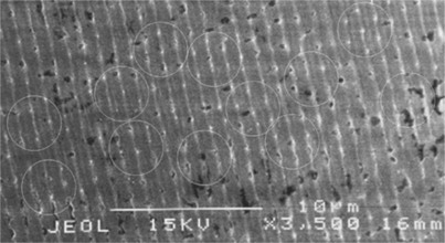
3.2 SEM image of the Ge single crystal surface irradiated by Nd:YAG laser at intensity 28 MW/cm2. C6i patterns are marked by white circles.
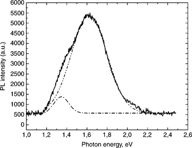
3.3 PL spectrum of the surface of Ge after irradiation by Nd:YAG laser at intensity up to 28 MW/cm2.
Photoluminescence in the IR, red, and blue-violet region of the spectra of Si and Ge nanoparticles implanted into SiO2 layer has been found by several scientific groups. Strong PL in the blue-violet region was achieved, with the values of excitation and emission energy being independent of the annealing temperature and, consequently, of the cluster mean size (Rebohle et al., 2000; Werwa et al., 1996). Different explanations of this PL mechanism have been proposed. One group of scientists explain the PL by QCE (Rebohle et al., 2000) in Si and Ge nanoparticles, but another group (Fernandez et al., 2002) by local Si-O and Ge-O vibration at Si-SiO2 and Ge SiO2 interface. A phonon confinement effect model was developed by Campbell and Fauchet (1986) for Si nanocrystals. It showed that by simultaneously using micro-Raman back scattering spectrum and PL spectrum, it is possible to determine the origin of the PL. It means, if ‘blue shift’ in PL spectrum and ‘red shift’ of LO line in Raman back scattering spectrum are simultaneously present, then QCE takes place in NSs. Therefore, this ‘blue shift’ in PL spectrum of Ge we can explain by the presence of QCE on the top of nanocones where the radius of the balls is equal or less than Bohr’s radii of electron and hole. Our calculation of the ball diameter on the top of nanocones using formula (1) from Efors and Efors (1982) and band gap shift from PL bands with maximums at 1.65 and 1.3 eV (Fowler et al., 1966) at parameters of Ge: me = 0.12 m0 and mh = 0.379 m0 for electron and hole effective masses, respectively, gives diameters of balls 4.0 and 6.0 nm.
An example of our suggestion is Raman back scattering spectra of the non-irradiated (curve 1) and of the irradiated (curve 2) surfaces of Ge crystal by the laser, as shown in Fig. 3.4. The line at 300 cm−1 of the non-irradiated surface of Ge is attributed to bulk Ge (Ge–Ge vibration, LO phonon line). ‘Red shift’ of the LO phonon line in Raman back scattering spectra by 6 cm−1 after irradiation of Ge surface takes place. The calculated position of line peak frequency of a Raman spectrum as a function of average crystal size (dave) for spherical Ge particles from Kartopu et al. (2004) corresponds to 4.0 nm diameter of Ge nanoball on the top of the nanocone. This value is in agreement with our calculation from formula [3.1] using the PL spectrum.

3.4 Micro Raman spectrum of the non-irradiated (curve 1) and of the irradiated surfaces of Ge single crystal by Nd:YAG laser (curve 2) at intensity up to 28 MW/cm2.
An AFM 3D image of the Si surface after irradiation by second harmonic of Nd:YAG laser at I = 2.0 MW/cm2 of SiO2/Si structure, and the same AFM 3D image of Si surface after subsequent wet etching by HF are shown in Figs. 3.5a and 3.5b respectively. Photoluminescence spectra of the irradiated (curves 1 and 2) and non-irradiated (curve 3) surface of SiO2/Si at intensity of LR up to 2.0 MW/cm2 are shown in Fig. 3.6. The surface morphology of SiO2 layer is smooth and ‘stone-block’ like, but in reality, under the SiO2 layer are very sharp Si nanocones, as shown in Fig. 3.5b, which arise on the SiO2/Si interface after irradiation by the laser.
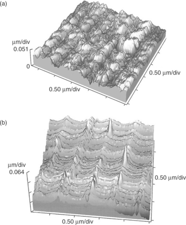
3.5 AFM 3D images of: (a) SiO2 surface after irradiation of SiO2/Si structure by Nd:YAG laser at I = 2.0 MW/cm2 and (b) Si surface after subsequent removing of SiO2 by HF acid.
3.6 Photoluminescence spectra of the SiO2/Si structure irradiated by the laser at intensity 2.0 MW/cm2 (2. and 3. curves), after removing of SiO2 layer by chemical etching in HF acid (3. curve). 1. curve corresponds to PL of the non-irradiated surface.
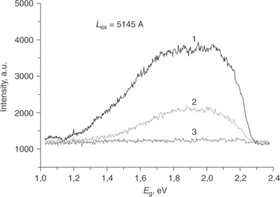
Photoluminescence of the SiO2/Si structure in the visible range of a spectrum with maximum at 2.05 eV obtained after irradiation by the laser at intensity I = 2.0 MW/cm2, as shown in Fig. 3.6, is unusual. The maximum band in PL spectrum is usually situated at 1.0 eV and the intensity of PL is very low due to the indirect band structure of Si crystals. PL of this structure after removal of the SiO2 layer by wet etching in HF acid is similar and is obtained in the same region of the spectrum and having the same positions of maximums. It means that PL is not connected with local Si-O vibration at the Si–SiO2 interface (Fernandez et al., 2002). Therefore, we explain our results by the QCE in nanocones. Decrease of the PL intensity can be explained by increase of reflection index of the structure after removal of the SiO2 layer. We can see that the visible PL spectrum of the SiO2/Si structure is wide and asymmetric with gradual decrease of intensity in IR range of the spectra. It is unique to PL spectrum typical for graded band gap structure. These results present a dramatic rise of PL intensity with a much higher band gap than for indirect Si. A schematic image of a nanocone with a gradual decrease in diameter from p-Si substrate till top is shown in Fig. 3.7. An increase of energy of a radiation quantum from substrate till top of the Si single crystal at PL of nanocone takes place due to the QCE in nanowire, according to this formula (Li and Wang, 2004):
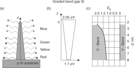
3.7 A schematic image of a nanocone with a gradually decreasing diameter from p-Si substrate till top, formed by laser radiation – (a) and (b). A calculated band gap structure of Si as a function of nanowires diameter using formula (2) from Li and Wang (2004) – (c).

where ![]() , (
, (![]() and
and ![]() are electron and hole effective-masses, respectively) and d is the diameter. For QWs, ζ = 2.4048. In our case, the diameter of nanocones/nanowires is a function of height d(z), therefore it is a graded band gap semiconductor. Our calculation of the Si band gap as a function of nanowires d from PL spectrum using formula (2) from Li and Wang (2004) is shown in Fig. 3.7. We can see that the dependence is nonlinear and that the function of diameter is decreasing, especially rapidly at small diameters. In our case the maximum band gap is 2.05 eV which corresponds to the minimal diameter 2.3 nm on the top of nanocones/nanowires.
are electron and hole effective-masses, respectively) and d is the diameter. For QWs, ζ = 2.4048. In our case, the diameter of nanocones/nanowires is a function of height d(z), therefore it is a graded band gap semiconductor. Our calculation of the Si band gap as a function of nanowires d from PL spectrum using formula (2) from Li and Wang (2004) is shown in Fig. 3.7. We can see that the dependence is nonlinear and that the function of diameter is decreasing, especially rapidly at small diameters. In our case the maximum band gap is 2.05 eV which corresponds to the minimal diameter 2.3 nm on the top of nanocones/nanowires.
We have found for the first time a method of forming a 1D graded band gap semiconductor structure. The graded change of band gaps arises due to the Quantum Confinement Effect. Usually, a 2D graded band gap semiconductor structure is formed by conventional methods, for example, by MBE (Voitsekhovskii et al., 2008), changing molecular components’ concentration layer by layer.
3.2.2 Experiments on Si1−x Gex/Si (X = 0.3; 0.4) and Cd1−x ZnxTe (X = 0.1) solid solutions
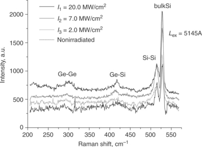
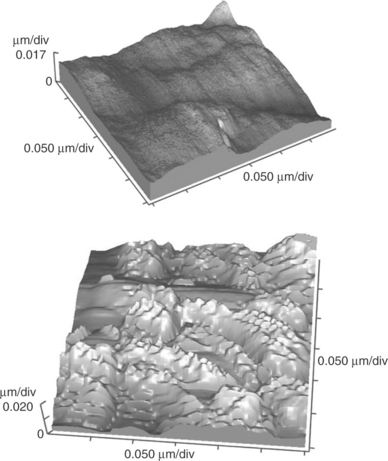
A 200 nm thick crystalline Si1−xGex alloy layer was grown on Si(100) wafers with a thickness of 150 μm by MBE on top of Si. Alloys containing 30% and 40% Ge were used in the experiments. The surface of an Si Ge/Si structure was irradiated by basic frequency of the Nd:YAG laser. The three-dimensional surface morphology of an Si1−xGex/Si hetero-epitaxial structure recorded by AFM measurements after irradiation by the Nd:YAG laser at intensities of 7.0 MW/cm2 (a) and 20.0 MW/cm2 (b) is shown in Fig. 3.8. Figure 3.8a shows the nanocones with an average height of 11 nm formed by LR at the intensity of 7.0 MW/cm2. Similar nanocones with an average height of 27 nm shown in Fig. 3.8b have been obtained by irradiation intensity of 20 MW/cm2. Due to higher irradiation intensity, they are higher and more compact in diameter. After irradiation of the Si Ge/Si hetero-epitaxial structure by the laser at an intensity of 7.0 MW/cm2 the surface structure begins to look like spots on unwetting material, for example, they look like water spots on a glass or ‘quick silver’ on a floor, as shown in Figs. 3.8c and 3.8d, respectively. It means that LR induces segregation of Ge phases at the irradiated surface of the sample due to drift and concentration of Ge atoms. This conclusion is in agreement with data from Kamenev et al. (2005) and Hartmann et al., (2005). It shows that the Ge phase starts to form at 50% concentration of Ge atoms in an SiGe solid solution.

3.8 Three-dimensional AFM images of Si1−x Gex/Si surfaces irradiated by the Nd:YAG laser at intensity (a) 7 MW/cm2 and (b) 20 MW/cm2 and two-dimensional surface morphology of the same spots of structure at intensities: (c) 7.0 MW/cm2 and (d) 20.0 MW/cm2.
According to the TGE (Medvid’, 2002), it is supposed that LR initiates the drift of Ge atoms toward the irradiated surface of the hetero-epitaxial structure (Medvid’ et al., 2009). PL spectra of the Si1−xGex/Si hetero-epitaxial structures with the maxima at 1.60–1.72 eV obtained after laser irradiation at intensities of 2.0, 7.0 and 20.0 MW/cm2 are shown in Fig. 3.9. The spectra are unique and unusual for the material because, depending on Ge concentration, the band gap of SiGe is situated between 0.67 and 1.12 eV (Sun et al., 2005). As seen in Fig. 3.9, the Si1−xGex structure emits light in the visible range of spectrum and the intensity of PL increases with the intensity of irradiation. The maximum of the PL band at 1.70 eV is explained by the QCE (Efors and Efors, 1982). Position of the observed PL peak compared with the bulk material shows a significant ‘blue shift’. The maxima of PL spectra of the Si1−xGex/Si hetero-epitaxial structure slightly shifts to higher energy when the laser intensity increases from 2.0 to 20.0 MW/cm2, which is consistent with the QCE too. Our suggestions concerning Ge phase formation are supported by the back scattering Raman spectra as shown in Fig. 3.10. After laser irradiation at the intensity of 20.0 MW/cm2, a Raman band at 300 cm−1 appears in the spectrum. This band is attributed to the Ge–Ge vibration and is explained by formation of a new Ge phase (Kamenev et al., 2005) in the Si1−xGex/Si hetero-epitaxial structure. It is proposed to use modified formula (3) from Efors and Efors (1982) for determination of concentration x in the nanocones of Si1−xGex/Si hetero-epitaxial structure formed by LR using PL spectra.

3.9 PL spectra of S0.7Ge0.3/Si hetero-epitaxial structures before and after irradiation by Nd:YAG laser.
3.10 Back scattering Raman spectra of SixGe1−x/Si hetero-epitaxial structure before and after irradiation by the laser. Appearance of the 300 cm−1 Ge–Ge vibration band in Raman spectra is explained by the new phase formation in SixGe1−x/Si hetero-epitaxial structure.
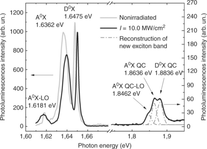
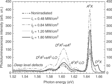
Nanocone formation on a surface of CdxZn1−xTe solid solution with x = 0.1 after irradiation by strongly absorbed Nd:YAG LR with intensity I = 12.0 MW/cm2 was observed using AFM, as shown in Fig. 3.11. Studying the nanocones’ optical properties, a new exciton band at energy up to 1.87 eV in the PL spectrum was seen for the first time. At the same time, a shift of A0X and D0X exciton lines on 3.1 and 2.5 meV correspondingly, toward the higher energy of quantum, that is the so-called ‘blue shift’, was observed, as shown in Fig. 3.12. Appearance of a new PL band is explained by Exciton Quantum Confinement (EQC) effect in nanocones and the ‘blue shift’ of the exciton bands – basically by mechanical compressive stress of the sample top layer formed on the irradiated surface of the samples. This process is described in the following way: irradiation of the Cd1−xZnxTe solid solution by the laser leads to the drift of Cd atoms toward irradiated surface and of Zn atoms – in the bulk of the semiconductor due to high gradient of temperature, the so-called TGE (Medvid’, 2002). As a result, formation of a ![]() Te hetero-structure, where x1 > x, takes place due to replacement of Zn atoms by Cd atoms at the irradiated surface. At the same time, the opposite process takes place under the top layer, in the buried layer of the semiconductor – Zn atoms replace Cd atoms. At least three factors determine A0X and D0X exciton lines position in PL spectrum. They are: concentration of Zn atoms in CdTe top layer and in CdZnTe buried layer (Reno and Jones, 1992), 2D EQC effect in the CdTe top layer when its thickness is comparable with Bohr’s radius of exciton, and mechanical compressive stress of the CdTe top layer due to mismatch of CdTe and CdZnTe crystalline lattice. Decrease of the Zn atoms concentration in the top layer with an increase of LR intensity, according to the proposed model, leads to the ‘red shift’ of the exciton bands in PL spectra, as shown in Medvid’ et al. (2007b), but increase of the Zn atoms concentration in buried CdZnTe layer manifests in ‘blue shift’ of the PL spectrum, as shown in Fig. 3.13. These effects do not compensate each other because they take place in different layers. This unusual situation can be explained by different input of these layers in the intensity of PL spectrum. If the top layer is excited by short wavelength light, then the ‘red shift’ of PL spectrum will be mostly observed, but if mainly the buried layer is excited, for example due to small thickness or transparency of top layer, then the ‘blue shift’ will be observed.
Te hetero-structure, where x1 > x, takes place due to replacement of Zn atoms by Cd atoms at the irradiated surface. At the same time, the opposite process takes place under the top layer, in the buried layer of the semiconductor – Zn atoms replace Cd atoms. At least three factors determine A0X and D0X exciton lines position in PL spectrum. They are: concentration of Zn atoms in CdTe top layer and in CdZnTe buried layer (Reno and Jones, 1992), 2D EQC effect in the CdTe top layer when its thickness is comparable with Bohr’s radius of exciton, and mechanical compressive stress of the CdTe top layer due to mismatch of CdTe and CdZnTe crystalline lattice. Decrease of the Zn atoms concentration in the top layer with an increase of LR intensity, according to the proposed model, leads to the ‘red shift’ of the exciton bands in PL spectra, as shown in Medvid’ et al. (2007b), but increase of the Zn atoms concentration in buried CdZnTe layer manifests in ‘blue shift’ of the PL spectrum, as shown in Fig. 3.13. These effects do not compensate each other because they take place in different layers. This unusual situation can be explained by different input of these layers in the intensity of PL spectrum. If the top layer is excited by short wavelength light, then the ‘red shift’ of PL spectrum will be mostly observed, but if mainly the buried layer is excited, for example due to small thickness or transparency of top layer, then the ‘blue shift’ will be observed.
3.11 Atomic force microscope 3D images of the Cd1−xZnxTe (x = 0.1) surfaces: (a) before irradiation and (b) after irradiation by the laser at intensity of 12 MW/cm2.
3.12 Photoluminescence spectra of the Cd1−xZnxTe (x = 0.1) measured at temperature 5 K: curve 1 before and curve 2 after irradiation by the laser at I = 10.0 MW/cm2.

Of course, it is possible to observe both PL spectra simultaneously at intermediate situations. Exactly such a situation is observed in the PL spectrum shown in Fig. 3.12, after destruction of the CdTe top layer and formation of nanocones on the irradiated surface of the sample. Relaxation of the mechanical compressive stress in the CdTe layer comes to expression as self-assembly of nanocones on the irradiated surface of the structure like Stranski–Krastanov’s mode, and simultaneous appearance of a new exciton band at 1.872 eV in PL spectrum at high intensity of LR takes place. Reconstruction of this band shows that it consists of three lines which look like A0X, D0X and A0X–LO lines (the distance between the lines and their relation intensities are the same) in the non-irradiated PL spectrum of the semiconductor. Therefore, we connect the appearance of both the new band in PL spectrum and the nanocones’ formation on the irradiated surface of the semiconductor with EQC in nanocones and denote them as A0XQC and D0XQC lines. Evidence of the mechanical stress relaxation process in the CdTe layer is non-monotonic dependence of the ‘blue shift’ as function of LR intensity, as shown in Fig. 3.13. Such non-monotonic dependence has been observed in p- and n-type Si after studying mechanical microhardness of Si after irradiation by Nd:YAG laser (Medvid’ et al., 2007b). Calculation of the mechanical compressive stress in the CdTe top layer using the maximum of the ‘blue shift’ of A0X exciton line from Fig. 3.13 and dEg/dP = 10 eV/Pa (Thomas, 1961), where Eg and P are the band gap of the CdTe crystal and mechanical stress respectively, gives P = 4.62 × 10⁵ Pa. This value corresponds to the ultimate strength limit of CdTe (Yonenaga, 2005). Calculation of the quantum dot diameter using the formula from Kayanuma (1988) and the ‘blue shift’ of A0XQC line in PL spectrum on 0.27 eV gives the diameter of the quantum dots up to 10.0 nm. This data corresponds to the size of nanocones (height and diameter of the bottom of the cones are 10.0 nm) measured using 3D image of AFM. Evidence of the presence of the EQC effect in nanocones is the decrease of LO phonon energy by 0.7 meV in the PL spectrum, that is the so-called phonon QCE (Campbell and Fauchet, 1986). Our calculation of the Zn atom’s distribution depending on intensity of LR using the thermo-diffusion equation has shown that the process of ![]() Te heterostructure formation is characterized by gradual increase of Zn atom’s concentration in the buried layer with intensity of LR up to 8% (x1 = 0.18). The thickness of the CdTe layer after irradiation by a laser with intensity of I = 12.0 MW/cm2 becomes 10 nm. Therefore, we explain that the A0X and D0X lines do not return to their initial position in the PL spectrum by increase of Zn atoms concentration in buried layer till x = 0.18.
Te heterostructure formation is characterized by gradual increase of Zn atom’s concentration in the buried layer with intensity of LR up to 8% (x1 = 0.18). The thickness of the CdTe layer after irradiation by a laser with intensity of I = 12.0 MW/cm2 becomes 10 nm. Therefore, we explain that the A0X and D0X lines do not return to their initial position in the PL spectrum by increase of Zn atoms concentration in buried layer till x = 0.18.
We connect the appearance of both the new band in PL spectrum and the nanocones formation on the irradiated surface of the semiconductor with EQC effect in nanocones and denote them as A0XQC and D0XQC lines. The process of nanocone formation is characterized by LR threshold intensity up to I = 9.0 MW/cm2, as we can see in Fig. 3.13, maximum of ‘blue shift’ position VS the laser intensity.
3.3 Two-stage mechanism of nanocones formation in semiconductors
We propose the following method of nanocone formation on the irradiated surface of GexSi1−x and CdxZn1−xTe solid solutions. The mechanism is characterized by two stages – laser redistribution of atoms (LRA) and selective laser annealing (SLA) (Medvid’ et al., 1996, 1997; Yonenaga, 2005). The first stage of the process, LRA, involves the formation of heterostructures, such as Ge/Si due to the separation of Ge and Si atoms in a GexSi1−x sample and ![]() Te in
Te in ![]() Te (x1 > x0) solid solutions due to the separation of Cd and Zn atoms in the gradient of temperature. The dominant phenomenon in this process is the thermogradient effect (Medvid’, 2002). The second stage, SLA, involves the formation of nanocones on the irradiated surface of a semiconductor. The heating of the structure, followed by the mechanical plastic deformation of the strained top layer leads to the formation of nanocones. The mechanical plastic deformation is caused by the relaxation of the mechanical compressive stress arising between these layers, owing to a mismatch of their crystal lattices and selective laser heating of the top layer. SLA occurs due to the higher absorption of the LR by the top layer than the buried layer. LRA is a nonlinear optical process: the concentration of the redistributed atoms (Ge in the case of GexSi1−x and Cd in the case of CdxZn1−xTe) increases with the number of laser pulses and at the same time, its absorption coefficient increases. As a result, the LRA stage gradually transits to the SLA stage. In the case of the elementary semiconductors, at the first stage of the process a thin top layer with a high concentration of interstitial atoms and mechanically compressive stress is formed on the irradiated surface of the semiconductor. For example, as shown in Fig. 3.14 for n-Si crystal, mechanical compressive stress increases with laser intensity at the first stage of the process (III band). This process takes place due to separation of interstitials and vacancies in the gradient of temperature field. Mechanical compressive stress of the top layer arises due to the presence of additional interstitials in the top layer and vacancies in the buried layer. At the second stage of the process, nanocones are formed on the irradiated surface of the semiconductor by plastic deformation of the top layer, mostly due to absorption of light by the top layer and therefore heating up. The cause of high absorption of light by the top is mechanical compressive stress which leads to a decrease of the semiconductor band gap (Kayanuma, 1988) and, of course, the increase of the absorption coefficient. Examples of the two-stage mechanism of nanocone formation on a surface of the semiconductors by LR are the following:
Te (x1 > x0) solid solutions due to the separation of Cd and Zn atoms in the gradient of temperature. The dominant phenomenon in this process is the thermogradient effect (Medvid’, 2002). The second stage, SLA, involves the formation of nanocones on the irradiated surface of a semiconductor. The heating of the structure, followed by the mechanical plastic deformation of the strained top layer leads to the formation of nanocones. The mechanical plastic deformation is caused by the relaxation of the mechanical compressive stress arising between these layers, owing to a mismatch of their crystal lattices and selective laser heating of the top layer. SLA occurs due to the higher absorption of the LR by the top layer than the buried layer. LRA is a nonlinear optical process: the concentration of the redistributed atoms (Ge in the case of GexSi1−x and Cd in the case of CdxZn1−xTe) increases with the number of laser pulses and at the same time, its absorption coefficient increases. As a result, the LRA stage gradually transits to the SLA stage. In the case of the elementary semiconductors, at the first stage of the process a thin top layer with a high concentration of interstitial atoms and mechanically compressive stress is formed on the irradiated surface of the semiconductor. For example, as shown in Fig. 3.14 for n-Si crystal, mechanical compressive stress increases with laser intensity at the first stage of the process (III band). This process takes place due to separation of interstitials and vacancies in the gradient of temperature field. Mechanical compressive stress of the top layer arises due to the presence of additional interstitials in the top layer and vacancies in the buried layer. At the second stage of the process, nanocones are formed on the irradiated surface of the semiconductor by plastic deformation of the top layer, mostly due to absorption of light by the top layer and therefore heating up. The cause of high absorption of light by the top is mechanical compressive stress which leads to a decrease of the semiconductor band gap (Kayanuma, 1988) and, of course, the increase of the absorption coefficient. Examples of the two-stage mechanism of nanocone formation on a surface of the semiconductors by LR are the following:
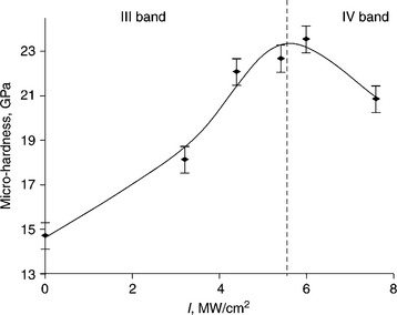
1. Non-monotonic dependence of Si crystal micro-hardness as a function of the laser intensity. There is an increase of the crystal micro-hardness at the LRA stage of laser irradiation and decrease of it at the LSA stage, as shown in Fig. 3.14, III and IV bands respectively.
2. An example of the presence of the first stage is the appearance and growth of LO phonon line intensity with a frequency of 300 cm−1 in the Raman back scattering spectrum of GexSi1−x solid solution after irradiation by the laser. It means formation of a new Ge phase on the irradiated surface of GexSi1−x (Medvid’ et al., 2010a), as shown in Fig. 3.10.
3. The shift of the PL spectrum of a CdxZn1−xTe solid solution at a low intensity of LR toward lower energy of quantum – the ‘red shift’ (Medvid’ et al., 2007b) – is the next evidence of the first stage of thin CdxZn1−xTe layer formation.
4. Appearance of nanocones on the irradiated surface of GexSi1−x solid solution and their growth with the laser intensity has been found by measurements of the irradiated surface morphology by AFM, as shown in Fig. 3.8.
5. The shift of bands in the PL spectrum of a CdxZn1−xTe solid solution at a high intensity of LR toward higher energy of quantum – the ‘blue shift’ – and appearance of a new PL band at higher energy of quantum – EQC Effect, as shown in Fig. 3.12, are evidence of the second stage of the mechanism.
6. The ‘blue shift’ of the PL spectra and increase of the PL bands intensity of Si, Ge, GexSi1−x and CdxZn1−xTe crystals with increasing intensity of the laser due to QCE, for example as shown in Fig. 3.9 for GexSi1−x crystal, is the next evidence of the LSA stage.
7. Evidence of the first stage presence at nanocones formation process is the redistribution of intensity of LO-ZnTe, TO-CdTe and LO-CdTe phonon lines in Raman back scattering spectra, as shown in Fig. 3.15. It means that before irradiation of the sample by the laser intensity of LO-ZnTe, the phonon line was 3–4 times higher than the intensity of TO and LO-CdTe phonon lines but after irradiation, the opposite is observed in Raman spectra.

3.4 Applications in nanoelectronics and optoelectronics
3.4.1 High intensity Si source of white light and photon detector with selective or ‘bolometer’ type of spectral sensitivity on the base of nanocones
A result of investigation into PL spectra of Si and GexSi1 – x crystals has shown, in Figs. 3.2 and 3.9, that nanocones radiate a wide spectrum of light quantum like the sun or a glow lamp. At the same time, this structure can be used as a photon detector with a ‘bolometer’ type of spectral photo sensitivity (Capasso, 1987), as shown in Fig. 3.16, curve 1. If irradiation of the structure takes place from the wide band gap part of a semiconductor with a gradient band gap structure, it means from the top of cones, or as a photon detector with selective type of spectral photo sensitivity, if irradiation of the structure takes place from narrow band gap part of graded band gap structure, as shown in Fig. 3.16, curve 2. Schematically graded band gap structure is shown in Fig. 3.16.
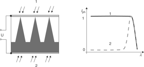
3.16 Scheme of photodetector with graded band gap structure and photoconductivity specters of photodetector with ‘bolometric’ type of photosensitivity – curve 1 (detector irradiate from nanocones side 1) and photodetector with selective type photosensitivity – curve 2 (detector irradiate from base side 2).
3.4.2 X- and γ-ray detector with increased radiation hardness
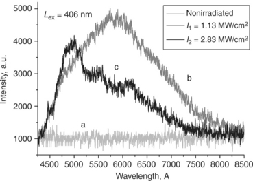
This part of the work deals with studying the possibility of increasing the radiation hardness of CdZnTe crystals using LR (Medvid’ et al., 2010b). An Nd:YAG laser with the following parameters – second harmonic and intensity range I = 0.5–2.0 MW/cm2– – was used as a source of light. This method of PL was used in the experiments for estimation of crystalline lattice damage after irradiation by gamma rays. Cd0.9Zn0.1Te crystal was the object of investigation. It is known that γ-radiation causes intrinsic defect generation in a semiconductor. The effect consists of an increase of the A0X exciton line in the PL spectrum of CdZnTe by ten times after γ-irradiation by 60Co source (E = 1.2 MeV) at room temperature with a dose of 5 × 10⁵ Rad = 5 kGy, as shown in Fig. 3.17, curves 1 and 3. Experimental results showed that this effect is suppressed by five times in CdZnTe crystals after preliminary irradiation by the laser at an intensity of more than 2.0 MW/cm2, as shown in Fig. 3.17, curve 4. The decrease of the A0X exciton line intensity in the PL spectrum indicates the decrease of generation of Cd vacancies in CdZnTe after preliminary irradiation by the laser. The mechanism of this effect is explained in the following way: γ radiation leads to generation of additional Cd vacancies near the surface layer (Xia and Yang, 2003), which causes an increase of the A0X exciton line in the PL spectrum. Laser radiation has the opposite effect on Cd0.9Zn0.1Te crystals: interstitial Cd atoms are concentrated near the irradiated surface layer, but vacancies in the bulk of the semiconductor (Medvid’, 2002). This leads to an A0X line decrease and increase of the D0X exciton line in the PL spectrum, as shown in Fig. 3.18. An increase in Cdi atom concentration near the surface layer leads to an increase of the materials radiation hardness due to two facts: that Cd atomic weight is larger compared to other atoms – Zn and Te, and ‘healing’ of the crystal lattice by Cdi atoms – recombination Vcd and Cdi.
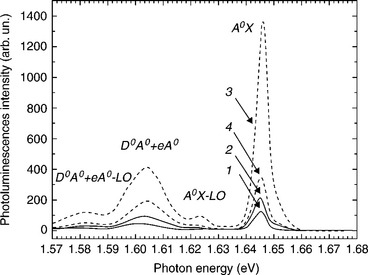
3.17 The PL spectra of Cd1−xZnxTe crystal before (curve 1) and after irradiation by Nd:YAG laser: curve 2 – irradiated by Nd:YAG laser with intensity 1.20 MW/cm2; curve 3 – irradiated by γ-ray with a dose rate of 5.0 KGy; curve 4 – previously irradiated by Nd:YAG laser with intensity 1.20 MW/cm2 and subsequently by γ-ray with a dose rate of 5.0 KGy.
3.4.3 Electron field emitter on the base of Si nanocones
Nanocones have been formed on the irradiated surface of p-Si crystals by the second harmonic of Nd:YAG laser with an intensity of 2.0 MW/cm2. The measurements of electron field emissions were performed with a flat diode configuration with a glass spacer (Evtukh et al., 2010). Distance between the cathode (silicon wafer) and the anode was 0.8 mm. The applied field emission setup allows achieving a vacuum of 1 × 10⁻⁵ Pa. The applied voltage varied between 1500 and 3600 V. The current–voltage characteristics of field emission current and corresponding curves in Fowler–Nordheim plots (lgI/E2 – 1/E) are shown in Fig. 3.19. The electron field emission from such nanocones have some peculiarities, namely: (i) decrease of the threshold field from Eth = 4 × 10⁴ V/cm at the first measurement to Eth = 3.5 × 10⁴ V/cm in subsequent measurements, (ii) two slopes of Fowler–Nordheim curves (higher slope at low fields and lower slope at high fields) (Fig. 3.19). Analysis of the SEM micrographs and electron field emission curves allows us to estimate (i) the electron field enhancement coefficient, β≈100, (ii) work functions (Φ1 = 6.8 eV at the first measurement and Φ2 = 3.9 eV, Φ3 = 2.38 eV from the two slopes in subsequent measurements), (iii) effective emission area, α = 3 × 10⁻⁸ – 1.8 × 10⁻⁵ cm2. The obtained experimental results were explained in the frame of the proposed model which takes into account formation of native oxide and/or positive dipoles (Si+–O−) due to oxygen adsorption on the Si surface. An improvement in the field emission after the first measurement may be due to the oxygen thermal field desorption or the transformation of the native oxide caused by a stress-induced leakage current process. As in metal-insulator-Si structures, the resistance of the thin oxide is reduced as a result of the current being passed through. The lower work function in relation to the known value for high doped n-type silicon Φ0 = 4.15 eV is explained by an increase of Si band gap on the top of nanocones, as shown in Fig. 3.7.

3.4.4 Third generation solar cells on the base of ITO/Si/Al structure
ITO/p-Si/Al structures, where the ITO top layer was 70 nm thick, an Si layer with a thickness of 500 μm and an Al back layer with a thickness of 100 nm in the experiments were studied. The structure was irradiated from the ITO side by an Nd:YAG LR second harmonic with a wavelength of λ = 512 nm and a pulse duration of τ = 10 ns. The diameter of the laser beam spot was 0.9 mm. Irradiation of the samples in the scanning regime using a two coordinate manipulator with a 20 μm step was carried out. Experiments in ambient atmosphere at a pressure of 1 atm, T = 20°C, and 60% humidity were performed.
The irradiated structures were studied using AFM and PL spectroscopy methods. The measurements of current–voltage (I–V) characteristics to observe the changes of electrical parameters for ITO/p-Si/Al structure after irradiation by laser were carried out. ITO/p-Si/Al structure has been irradiated by an Nd:YAG laser with the aim of forming a p-n junction on the interface of ITO/Si and to grow nanocones on the interface of ITO/Si in which QCE takes place (Medvid’ et al., 2011). The n-type Si layer was formed on p-type Si due to drift of interstitial Si atoms toward the irradiated surface, as a result of huge gradient of temperature induced by LR (Medvid’, 2002).
Nanocones were formed on the irradiated Si surface with an average height of 30 nm by LR with an intensity of up to 2.83 MW/cm2 as shown in Fig. 3.20. PL spectra of the ITO/p-Si structures with the maxima at 575 and 490 nm obtained after laser irradiation at intensities of 1.13 and 2.83 MW/cm2 are shown in Fig. 3.21. Position of the observed PL peak compared with the bulk Si shows a significant ‘blue shift’. The maxima of the PL band at 575 and 490 nm are explained by presence of the QCE (Medvid’ et al., 2011) on the top of the nanocones. After irradiation of the ITO/p-Si/Al structure by the laser, photocurrent power increased twofold in comparison to the non-irradiated structure. This effect is explained by QCE in nanocones. It means that the Si band gap is increased with the increase of the laser intensity. It is found that the dark I–V characteristic becomes diode-like with a rectification coefficient of K = 105 at 5 V caused by the laser irradiation with a intensity of I2 = 2.83 MW/cm2 as shown in Fig. 3.22. The improvements of the ITO/p-Si/Al structure as a solar cell can be explained by the increase of potential barriers between ITO and p-Si layers.

3.20 AFM images of ITO/p-Si structure irradiated by Nd:YAG laser: boarder of non-irradiated – smooth surface and irradiation by Nd:YAG laser at intensity 2.83 MW/cm2 – surface with nanocones.

3.5 Conclusions
For the first time, a method for the formation of 1D graded band gap semiconductor structures has been found. Graded change of band gap arises due to the QCE in nanocones.
A new PL exciton band with energy of up to 1.87 eV was found in the PL spectrum of Cd1−x ZnxTe solid solution after irradiation by a Nd:YAG laser second harmonic with an intensity of 12.0 MW/cm2. Appearance of the PL exciton band is explained by exciton QCE in nanocones which were formed by LR. Two-stage mechanism of nanocones formation on a surface of the semiconductor by Nd:YAG LR consisting of laser redistribution of atoms and SLA is proposed. Possibility to control heterostructure parameters, for example, thickness, by LR intensity, which is the first stage of the process, is shown. The power of ITO/p-Si/Al solar cell structure has been increased twofold after irradiation by Nd:YAG laser second harmonic with intensity 2.83 MW/cm2 due to formation of Si nanocones with p-n junction on their top. A twofold decrease of work function of electrons from Si nanocones formed by Nd:YAG laser second harmonic with intensity 2.0 MW/cm2 is explained by increase of Si band gap on the top of nanocones due to QCE.
3.6 Acknowledgements
The author gratefully acknowledges financial support in part by Europe Project in the framework FR7-218000 ‘COCAE’, ERAF Project ‘Sol-gel and laser technologies for the development of nanostructures and barrier structures’, No.2010/0221/2DP/2.1.1.0/10/AP IA/VIAA/145, the ESF Project No. 1DP/1.1.1.2.0/09/ APIA/VIAA/142, by the Latvian Council of Science according to the Grant 10.0032. 6.2 and the Riga Technical University project ZP-2010/19.
3.7 References
Alivisatos, A.P. Semiconductor clusters, nanocrystals, and quantum dots. Science. 1996; 271:933–937.
Beigelsen, D.K., Rozgonyi, G.A., Shank, C.V.Energy beam–solid interactions and transient thermal processing. Pittsburgh: Material Research Society, 1985.
Brus, L.E. Electron–electron and electron–hole interactions in small semiconductor crystallites: The size dependence of the lowest excited electronic state. Journal of Chemical Physics. 1984; 80:4403–4409.
Campbell, H., Fauchet, P.M. The effects of microcrystal size and shape on the one phonon Raman spectra of crystalline semiconductors. Solid State Communications. 1986; 58:739–774.
Capasso, F., Graded-gap and superlattice devices by bandgap engineeringDingle, R., eds. Semiconductors and semimetals; Volume 24. At&T Bell Laboratories Murray Hill, New Jersey, 1987:319–395.
Carini, G.A., Bolotnikov, A.E., Camarda, G.S., James, R.B. High-resolution X-ray mapping of CdZnTe detectors. Nuclear Instruments and Methods in Physics Research A. 2007; 579:120–124.
Efors, A.L., Efors, A.L. Band-band absorption of light in semiconductor ball. Physics and Technics of Semiconductors. 1982; 16:1209–1214. [(in Russian)].
Emel’yanov, V.I., Panin, I.M. Defect-deformational self-organization and nanostructuring of solid surfaces. Solid State Physics. 1997; 39:2029–2035.
Evtukh, A., Medvid’, A., Onufrijevs, P., Okada, M., Mimura, H. Electron field emission from the Si nanostructures formed by laser irradiation. Journal of Vacuum Science & Technology B. 2010; 28:C2B11. [C2B13].
Fernandez, B.G., Lopez, M., Garcia, C., Perez-Rodriguez, A., Morante, J.R., Bonafos, C., Carrada, M., Claverie, A. Influence of average size and interface passivation on the spectral emission of Si nanocrystals embedded in SiO2. Journal of Applied Physics. 2002; 91:789–793.
Fowler, A.B., Fang, F.F., Howard, W.E., Stiles, P.J. Magneto-oscillatory conductance in silicon surfaces. Physical Review Letters. 1966; 16:901–903.
Fujisawa, I. Type conversion of InSb from p to n by ion bombardment and laser irradiation. Japanese Journal of Applied Physics. 1980; 19:2137–2140.
Furukawa, S., Miyasato, T. Quantum size effects on the optical band gap of microcrystalline Si:H. Physical Review B. 1988; 38:5726–5729.
Gnatyuk, V.A., Aoki, T., Hatanaka, Y., Vlasenko, O.I. Defect formation in CdTe during laser-induced doping and application to the manufacturing nuclear radiation detectors. Physica Status Solidi (c). 2006; 1:121–124.
Green, M.A.Third generation photovoltaics: Advanced solar emerge conversion. Berlin: Springer-Verlag, 2004.
Gupta, A., Viral, P., Compaan, L., Alvin, D. High efficiency ultra-thin sputtered CdTe solar cells. Solar Energy Materials & Solar Cells. 2006; 90:2263–2271.
Hartmann, J.M., Bertin, F., Rolland, G., Semeria, M.N., Bremond, G. Effects of the temperature and of the amount of Ge on the morphology of Ge islands grown by reduced pressure–chemical vapor deposition. Thin Solid Films. 2005; 479:113–120.
Kamenev, B.V., Baribeau, J.-M., Lockwood, D.J., Tsybekov, A. Optical properties of Stranski-Krastanov grown three-dimensional Si/Ge nanostructures. Physica E. 2005; 26:174–178.
Kartopu, G., Bayliss, S.C., Hummel, R.E., Ekinci, Y. Report on the origin of the orange PL emission band. Journal of Applied Physics. 2004; 957:2466–2472.
Kayanuma, Y. Quantum-size effects of interacting electrons and holes in semiconductor microcrystals with spherical shape. Physical Review B. 1988; 38:9797–9805.
Kurbatov, L., Stojanova, I., Trohimchuk, P.P., Trohin, A.S. Laser annealing of AIIIBV compound. Report Academy of Science USSR. 1983; 268:594–597.
Li, J., Wang, L.W. Comparison between quantum confinement effects of quantum wires and quantum dots. Chemistry of Materials. 2004; 16:4012–4015.
Mada, Y., Ione, N. p-n junction formation using laser induced donors in silicon. Applied Physics Letters. 1986; 48:1205–1207.
Medvid’, A. Redistribution of the point defects in crystalline lattice of semiconductor in nonhomogeneous temperature field. Defects and Diffusion Forum. 2002; 210–212:89–101.
Medvid’, A., Fedorenko, L. Generation of donor centers in p-InSb by laser radiation. Materials Science Forum. 1999; 297–298:311–314.
Medvid’, A., Lytvyn, P. Dynamics of laser ablation in SiC. Materials Science Forum. 2004; 457–460:411–414.
Medvid’, A., Dmytruk, I., Onufrijevs, P., Pundyk, I. Quantum confinement effect in nanohills formed on a surface of Ge by laser radiation. Physica Status Solidi (c). 2007; 4:3066–3069.
Medvid’, A., Fedorenko, L., Korbutjak, B., Kryluk, S., Yusupov, M., Mychko, A. Formation of graded band-gap in CdZnTe by YAG:Nd laser radiation. Radiation Measurements. 2007; 42:701–703.
Medvid’, A., Fedorenko, L., Snitka, V. The mechanism of generation of donor centres in p-InSb by laser radiation. Applied Surface Science. 1999; 142(142):280–285.
Medvid’, A., Fukuda, Y., Michko, A., Onufrievs, P., Anma, Y. 2D lattice formation on a surface of Ge single crystal by YAG:Nd laser. Applied Surface Science. 2005; 244(1–4):120–123.
Medvid’, A., Hatanaka, Y., Korbutjak, D., Fedorenko, L., Krilyuk, S., Snitka, V. Generation of the A-centres at the surface of CdTe(Cl) by YAG:Nd laser radiation. Applied Surface Science. 2002; 197–198:124–129.
Medvid’, A., Kaupuzs, J., Madzulis, I., Blms, J. Buried layer formation in silicon by laser-radiation. Journal of Applied Physics. 1996; 79:9118–9122.
Medvid’, A., Knite, M., Kaupuzs, J., Frishfelds, V. Mechanism of recording and erasing of optical information by laser radiation on SiO2-(Co+Si)-SiO2-Si multilayer structure. Applied Surface Science. 1997; 115:393–398.
Medvid’, A., Litovchenko, V.G., Korbutjak, D., Fedorenko, L.L., Hatanaka, Y. Influence of laser radiation on photoluminescence of CdTe. Radiation Measurements. 2001; 33:725–729.
Medvid’, A., Mychko, A., Strilchyuk, O., Litovchenko, N., Naseka, Y., Onufrijevs, P., Pludonis, A. Exciton quantum confinement effect in nanostructures formed by laser radiation on the surface of CdZnTe ternary compound. Physica Status Solidi (c). 2008; 6:209–212.
Medvid’, A., Mychko, A., Gnatyuk, V.A., Levytskui, S., Naseka, Y. Mechanism of nanostructure formation on a surface of CdZnTe crystal by laser irradiation. Journal of Automation, Mobile Robotics & Intelligent Systems. 2009; 3:127–129.
Medvid’, A., Onufrijevs, P., Chiradze, G., Muktupavela, F. Impact of laser radiation on microhardness of a semiconductor. AIP Conference Proceedings, 30th International Conference on the Physics of Semiconductors, July 25–30 338, Coex, Seoul, Korea, 2010.
Medvid’, A., Onufrievs, P., Dauksta, E., Barloti, J., Ulyashin, A., Dmytruk, I., Pundyk, I. P-n junction formation in ITO/p-Si structure by powerful laser radiation for solar cells applications. Advanced Materials Research. 2011; 222:225–228.
Medvid’, A., Onufrijevs, P., Dmitruk, I., Pundyk, I. Properties of nanostructure formed on SiO2/Si interface by laser radiation. Solid State Phenomena. 2008; 131–133:559–562.
Medvid’, A., Onufrijevs, P., Lyutovich, K., Oehme, M., Kasper, E., Dmitruk, N., Kondratenko, O., Dmitruk, I., Pundyk, I. Self-assembly of nanohills in SixGe1-x/Si by laser radiation. Journal of Nanoscience and Nanotechnology. 2010; 10:1094–1098.
Mooney, P.M., Jordan-Sweet, J.L., Ismail, K., Chu, J.O., Feenstra, R.M., LeGoues, F.K. Relaxed Si0.7Ge0.3 buffer layers for high-mobility devices. Applied Physics Letters. 1995; 67:2373–2375.
Morales, A.M., Lieber, C.M. A laser ablation method for the synthesis of crystalline semiconductor nanowires. Science. 1998; 279:208–211.
Rebohle, L., von Borany, F.J.H., Skorupa, W. Blue photo- and electroluminescence of silicon dioxide layers ion-implanted with group IV elements. Applied Physicas B: Lasers Optics. 2000; B70:131–134.
Reno, J., Jones, E. Determination of the dependence of the band-gap energy on composition for Cd1–x ZnxTe. Physical Review B. 1992; 45:1440–1442.
Sun, K.W., Sue, S.H., Liu, C.W. Visible photoluminescence from Ge quantum dots. Physica E. 2005; 28:525–530.
Talochkin, A.B., Teys, S.A., Suprun, S.P. Resonance Raman scattering by optical phonons in unstrained germanium quantum dots. Physical Review B. 2005; 72:115416–115423.
Thomas, D.G. Excitons and band splitting produced by uniaxial stress in CdTe. Journal of Applied Physics. 1961; 32:2298–2304.
Vigil-Galán, O., Arias-Carbajal, A., Mendoza-Pérez, R., Santana-Rodríguez, G., Sastre-Hernández, J., Alonso, J.C., Moreno-García, E., Contreras-Puente, G., Morales-Acevedo, A. Improving the efficiency of CdS/CdTe solar cells by varying the thiourea/CdCl2 ratio in the CdS chemical bath. Semiconductor Science and Technology. 2005; 20:819–822.
Voitsekhovskii, A.V., Grygor’ev, D.V., Smith, R. Radiation defect formation in graded-band-gap epitaxial structures Hg1–xCdxTe after boron ion implantation. Semiconductor Science and Technology. 2008; 23:1–7.
Vorobyev, L.E., Semiconductor parametersLevinshtein, M., Rumyantsev, S., Shur, M., eds. Handbook Series on Semiconductor Parameters; Vol. 1. World Scientific, London, 1996:33–57.
Werwa, E., Seraphin, A.A., Chiu, L.A., Zhou, C., Kolenbrander, K.D. Synthesis and processing of silicon nanocrystallites using a pulsed laser ablation supersonic expansion method. Applied Physics Letters. 1996; 64:1821–1825.
Xia, Y., Yang, Y. Chemistry and physics of nanowires. Advanced Materials. 2003; 15:351–353.
Yonenaga, I. Hardness, yield strength, and dislocation velocity in elemental and compound semiconductors. Materials Transactions. 2005; 46:1979–1985.
Yoshida, T., Yamada, Y., Orii, T. Electroluminescence of silicon nanocrystallites prepared by pulsed laser ablation in reduced pressure inert gas. Journal of Applied Physics. 1998; 83(10):5427–5432.
Zhao, Z.M., Yoon, T.S., Feng, W., Li, B.Y., Kim, J.H., Liu, J., Hulko, O., Xie, Y.H., Kim, H.M., Kim, K.B., Kim, H.J., Wang, K.L., Ratsch, C., Caflisch, R., Ryu, D.Y., Russell, T.P. The challenges in guided self-assembly of Ge and InAs quantum dots on Si. Thin Solid Films. 2006; 508:195–199.