
Multiphoton lithography, processing and fabrication of photonic structures
Abstract:
This chapter discusses the use of multiphoton fabrication techniques to create two- and three-dimensional photonic devices. After reviewing the basic principles of multiphoton lithography, the materials that can be patterned with multiphoton techniques are introduced. Examples of photonic devices created with multiphoton lithography are then presented, followed by a discussion of future prospects for multiphoton fabrication techniques in photonics.
5.1 Introduction to multiphoton lithography
New applications in photonics are increasingly demanding the ability to create devices with intricate, 3D structures that potentially involve multiple materials. The fabrication of such structures is often challenging, if not impossible, using conventional lithographic techniques. Multiphoton lithographic techniques are gaining considerable prominence for their ability to create complex, 3D structures for applications in photonics and beyond (Farsari et al., 2010; LaFratta et al., 2007; Maruo and Saeki, 2008; Yang et al., 2005).
The key to multiphoton lithography is that multiphoton absorption can be used to drive chemical or physical changes in extremely small (sub-fem-tolitre) volumes at precise locations in three dimensions. This localization arises through a combination of optical nonlinearity (the probability for multiphoton absorption depends nonlinearly on the intensity of the laser irradiation) and chemical nonlinearity (most photodeposition processes do not occur below a certain threshold exposure). The localized 3D patterning capability of multiphoton lithography allows for the deposition or removal of a wide range of different materials in 3D patterns with resolution that can be below 100 nm. The materials that can be deposited directly include polymers, inorganics and metals. In most cases, this deposition can be accomplished with just a few milliwatts of power from an ultrafast laser operating in the near-infrared region of the electromagnetic spectrum. Furthermore, with additional processing it is possible to coat or convert structures created with multiphoton lithography with a broad range of other materials for specific applications. Due to these unique capabilities, multiphoton lithography is being used for an increasing number of applications in photonics, such as in the creation of photonic crystals, metamaterials, waveguide-based devices, microoptics and optical data storage media.
In this chapter we will introduce the basic principles of multiphoton absorption and how it can be used for the high-precision, localized deposition of materials in three dimensions. We will then review the types of materials that can be patterned with multiphoton lithography, after which we will discuss applications of multiphoton lithographic techniques in photonics. The chapter finishes by discussing future prospects for 3D photonic devices created with multiphoton lithography.
5.2 Principles of multiphoton absorption and lithography
In this section we review some of the essential principles of multiphoton absorption and its application to 3D fabrication. We also specifically consider the optical and chemical effects that determine the overall resolution of multiphoton fabrication techniques.
5.2.1 Multiphoton absorption
In conventional (linear) optical absorption, the energy of an individual photon matches the energy gap between the ground state and an excited state of an atom or molecule (Fig. 5.1a). As a result of this energy match, the probability for absorption scales linearly with the light intensity. In multiphoton absorption, an individual photon does not have enough energy to drive an electronic transition. Instead, the transition is driven by two or more photons acting collectively (Fig. 5.1b). Because there is no intermediate resonant state reachable by linear absorption, multiphoton absorption proceeds through one or more virtual states. Thus, all of the photons needed for a multiphoton absorption event must be present in the same place at the same time. The absorption probability therefore scales as the light intensity to the power of the number of photons that are needed for the absorption event (typically two, but in some cases three or more).

5.1 (a) Energy-level scheme for linear absorption. (b) Energy-level scheme for two-photon absorption. (c) Total number of molecules excited in transverse planes for linear absorption with a focused laser beam, ignoring depletion of the beam intensity. (d) Total number of molecules excited in transverse planes for two-photon absorption with a focused laser beam.
Consider a laser beam that is focused tightly, as through a microscope objective (Fig. 5.1c). The total number of photons per unit time passing through a plane that is transverse to the direction of propagation of the beam is the same regardless of the position of the plane along the beam axis (z). However, because the beam is focused, the area of the plane of the beam (A) is a function of z. The intensity in a plane at height z (which we denote I(z)) is then inversely proportional to A(z). However, the number of molecules within the volume A(z) dz, which we will call N(z), is proportional to A(z). The total number of molecules excited in a plane at height z is proportional to the product of I(z) and N(z); this product is independent of A(z). Thus, with linear excitation, the total number of molecules excited in a plane at height z (which we denote Ne(z)) is independent of z (ignoring any decrease of the intensity along the beam path due to absorption).
Now consider the case of two-photon absorption (Fig. 5.1d). The square of the intensity in any transverse plane is inversely proportional to A2(z). N(z) is again proportional to A(z), so Ne(z) in this case is inversely proportional to A(z). Thus, the probability of exciting molecules with two-photon absorption is much greater at the laser focus than in any other region of the beam.
If a continuous-wave laser is used for two-photon absorption, its intensity generally must be very high in order to have a significant probability of having two photons in the same place at the same time in the focal region. Thus, two-photon absorption is typically driven with a laser that produces pulses with a duration in the range of 50 fs to 1 ps. For instance, a typical Ti:sapphire oscillator produces pulses at a wavelength near 800 nm with a duration on the order of 100 fs at a repetition rate on the order of 80 MHz. The duty cycle of such a laser is on the order of 10−5, so even when the peak intensity is high enough to drive two-photon absorption efficiently, the average power can still be quite low. Multiphoton fabrication is generally performed with an average laser power of a few milliwatts at the sample.
For an objective with a numerical aperture NA and a laser with wavelength λ, average power ![]() pulse length τ and repetition rate R, the number of photons absorbed per molecule per unit time is given approximately by (Denk et al., 1990)
pulse length τ and repetition rate R, the number of photons absorbed per molecule per unit time is given approximately by (Denk et al., 1990)
Here, ħ is Planck’s constant, c is the speed of light and δ is the two-photon-absorption cross-section. The units of δ are Göppert-Mayer (GM), in honor of Nobel laureate Maria Göppert-Mayer, who first predicted that two-photon absorption could occur. One GM unit is equal to 10–58 m4 s photon−1, and a typical dye molecule has a maximum δ value on the order of 1–100 GM. Molecules that are designed to have especially efficient two-photon absorption can have δ values that are as much as several orders of magnitude larger.
5.2.2 Resolution
Because multiphoton absorption has a nonlinear dependence on the light intensity, the effective point-spread function (PSF) for fabrication is smaller than the PSF for linear absorption at the same wavelength. Thus, multiphoton fabrication offers finer resolution than would otherwise be possible at the same wavelength. However, the resolution of the PSF is not superior to that available at the effective fabrication wavelength (e.g., half of the incident wavelength for two-photon absorption). Nevertheless, multiphoton absorption has a significant advantage over linear absorption in that molecules are excited only in the focal region. It is this effect that makes high-precision, 3D fabrication possible with multiphoton absorption.
In addition to optical nonlinearity, multiphoton lithography often also takes advantage of chemical nonlinearity. In many photochemical processes, there is a threshold exposure below which material is not deposited. As a result, the lithographic resolution of a multiphoton process can be considerably smaller than the diffraction-limited spot size of the laser beam, even when taking the optical nonlinearity into account.
As an example of the resolution obtainable with multiphoton fabrication, we will consider the most common multiphoton fabrication technique, multiphoton absorption polymerization (MAP, Fig. 5.2). If the laser beam is held in a fixed location while exposing a photoresist, a single volume element (‘voxel’) of polymer is created. In typical multiphoton photoresists, the best transverse resolution attainable with 800 nm light is on the order of 80 nm (Li et al., 2009; Xing et al., 2007). The ability to attain λ/10 resolution is attributable directly to the chemical nonlinearity of the photoresist. Resolution as fine as 20 nm using 800 nm excitation has been reported in special cases (Tan et al., 2007), but not for free-form fabrication. In addition, the use of a shorter excitation wavelength has been shown to be able to improve the resolution of MAP to 60 nm (Haske et al., 2007).

5.2 Representative structures created using MAP. (a) Letter M. (b) The word ‘hair’ written on a human hair. (reprinted with permission from Baldacchini et al., 2004)
Due to the geometry of the PSF, the axial dimension of voxels created with MAP is typically a factor of three to five larger than the transverse dimension (Fig. 5.3a). Thus, voxels are generally shaped like cucumbers. This voxel asymmetry can be a limitation in the fabrication of detailed structures that require fine resolution, such as photonic crystals.

5.3 (a) Typical voxel created with MAP (b) Resolution improvement attained using RAPID lithography as a function of deactivation power. (both reprinted with permission from Li et al., 2009)
To address the issue of voxel asymmetry and to improve the resolution of MAP, a technique called Resolution Augmentation through Photo-Induced Deactivation (RAPID) lithography has been developed (Li et al., 2009). RAPID lithography uses one laser to create a cross-linked polymer and a second laser to inhibit cross-linking. Through spatial phase shaping of the second laser beam to inhibit polymerization only in chosen regions, considerable improvements in resolution can be realized. For instance, voxels with a 40-nm axial dimension have been reported using 800-nm excitation, representing λ/20 resolution. In this case, the aspect ratio of voxels was reduced from the typical value of three to five down to one half (Fig. 5.3b). Further improvements in materials and optics for RAPID lithography promise to push the resolution down further, perhaps to the range of 20 nm or even smaller (Fourkas, 2010).
5.3 Materials for multiphoton lithography
In this section we review the types of materials that can be used for multiphoton lithography. We begin with a discussion of materials from which structures can be created directly. We then discuss the use of structures fabricated with multiphoton lithography as templates for the deposition of other materials.
5.3.1 Direct deposition
Direct deposition schemes use precursors that can be converted directly into the desired material using multiphoton absorption. The advantage of direct deposition is that the creation of devices typically requires a single fabrication step. However, the range of materials that can be deposited directly to form high-quality structures is somewhat limited. Nevertheless, direct deposition has found many uses in photonics, and here we will review some of the most important materials used in this type of fabrication.
Polymers
By far the most common multiphoton fabrication technique is MAP (LaFratta et al., 2007; Maruo and Fourkas, 2008; Yang et al., 2005). MAP typically employs a negative-tone photoresist that is hardened locally upon multiphoton excitation. MAP photoresists contain two key components: a cross-linkable monomer and a photoinitiator. Optical excitation of the photoinitiator starts a chain reaction through which monomers cross-link with one another, creating an insoluble polymer. Competing chemical processes limit the cross-linking reaction to regions with a sufficient concentration of excited initiator. After the desired 3D pattern has been scanned, the unexposed photoresist is removed by solvent development.
Two different types of negative-tone photoresist material have been employed widely for MAP. The first type is polymerized through a radical mechanism. Radical photoresists are typically composed of acrylic and/or methacrylic monomers (Baldacchini et al., 2004; Cumpston et al., 1999). Such monomers are widely available, and the properties of the final structures can be tuned in a straightforward manner by adjusting the composition of monomers used. Because radical polymerization takes place immediately upon excitation of a photoinitiator, structures created with these materials can be visualized during fabrication based on the change in refractive index caused by the cross-linking. This refractive index change can also lead to optical distortions that affect the fabrication of subsequent features, however, and so fabrication paths must be designed with care with these materials. Typical radical photoresists used for MAP are viscous liquids, which means that development can be accomplished with a few solvent washes. However, for photoresists that are liquids, flow during fabrication can also be an issue. Fillers that cause the resist to gel can circumvent this problem (Kuebler et al., 2001), although the solvent development of such materials is somewhat more difficult.
The other major type of negative-tone photoresist used for MAP is polymerized by a cationic mechanism. Cationic photoresists are typified by epoxies, such as SU-8 (Kumi et al., 2010; Witzgall et al., 1998). Cationic polymerization in MAP begins with the excitation of photoacid generator (PAG). Rather than leading to an immediate polymerization chain reaction, the photoresist typically must be brought to an elevated temperature following exposure to facilitate cross-linking. After this ‘postbake’ step, solvent development is used to remove the unpolymerized material. Because the majority of polymerization occurs during the postbake, cationic photoresists such as SU-8 do not generally exhibit significant changes in refractive index during fabrication. This facet of cationic photoresists helps to minimize any optical distortions, but also makes it difficult to ascertain the location of structures relative to the substrate during fabrication.
Numerous photoinitiators and PAGs have been developed over the years for use with linear excitation. These materials tend to be optimized for high initiation velocities and efficient generation of radicals or acid. Many of these materials have been shown to be suitable for MAP as well. However, these initiators are intended for linear excitation. In this case, having too high an absorption cross-section can be a disadvantage because it is difficult to expose thick films of photoresist. Thus, commercially available initiators do not tend to have large multiphoton absorption cross-sections at appropriate wavelengths (Yanez et al., 2009a). For this reason, some groups have focused on creating new photoinitiators or PAGs that have large δ values (Cumpston et al., 1999; Yanez et al., 2009a).These molecules typically allow MAP to be achieved at quite low intensities. However, due to the complexity of synthesizing these materials, as well as to solubility issues, the majority of researchers in the field still use commercially available components.
RAPID lithography requires a photoinitiator that can be excited by multiphoton absorption and deactivated by a second beam of light. To date, RAPID lithography has only been demonstrated for radical polymerization (Li et al., 2009; Stocker et al., 2011). Although the deactivation of one conventional photoinitiator has been reported using stimulated emission (Fischer et al., 2010), other common dye molecules that are not typically viewed as photoinitiators appear to be promising candidates for RAPID initiators that can be excited and deactivated (by another mechanism) with high efficiency (Stocker et al., 2011).
MAP can also be used to create patterns in positive-tone photoresists, that is, resists in which the exposed region can be removed by development, leaving the rest of the photoresist behind (Gansel et al., 2009; Yu et al., 2003; Zhou et al., 2002). The challenge in using positive-tone resists for creating 3D structures is that it is difficult to remove material from small regions that are deep inside of large structures. Because of this mass-transfer issue, positivetone photoresists have received far less attention than have negative-tone photoresists for MAP. Nevertheless, for some applications in photonics, positive-tone resists are advantageous and have been used.
Metals
Many applications in photonics, such as reflectors, gratings, photonic crystals and metamaterials, can benefit from the ability to deposit metals in three dimensions with nanoscale precision. As such, a considerable amount of effort has been put into the development of methods for the direct multiphoton deposition of metals. The creation of 3D metallic structures with multiphoton lithography presents significant materials challenges in comparison to the deposition of polymers. In the case of polymer fabrication, essentially 100% of the precursor (the photoresist) is converted to the final material (the cross-linked polymer). However, the deposition of metals relies on the photoreduction of metal ions, the dissociation of organometallic precursors, or the aggregation of nanoparticles by removing stabilizers. All of these processes leave organic byproducts. Furthermore, these precursors must generally be dispersed in another material. Thus, the fraction of the material that is converted in multiphoton metal deposition is typically considerably less than 100%.
One approach to multiphoton deposition of metallic structures is to begin with a liquid solution containing the precursor. A number of metals have been photodeposited from solution, including silver (Ishikawa et al., 2006; Tanaka et al., 2006), gold (LaFratta et al., 2007; Tanaka et al., 2006) and iron (LaFratta et al., 2007). Solution deposition with multiphoton absorption is generally best suited for the creation of 2D patterns. Because a relatively small fraction of any volume of the solution can be converted to metal, it is more difficult to create 3D structures. Often one must scan over areas repeatedly, leaving enough time between scans for additional precursor to diffuse into the region of interest. Deposition solutions are also prone to the formation of gas bubbles, either through boiling or decomposition of the precursor, which can lead to distortions in the shape of the final structure. Additionally, metallic structures with submicron feature sizes often do not have sufficient mechanical integrity for the creation of free-standing structures. However, the fabrication of 3D nanostructures by deposition of silver nanoparticles from solution has been demonstrated (Cao et al., 2009), although the fidelity of these structures does not yet approach what can be achieved for polymers with MAP.
Metal precursors can also be dispersed in polymer matrices for multiphoton deposition. This approach offers considerably greater latitude for the creation of 3D structures, especially if the polymer host need not be removed after fabrication. A number of groups have reported the creation of both 2D and 3D structures composed of metals such as silver and gold using polymer matrices (Baldacchini et al., 2005; LaFratta et al., 2006b; Maruo and Saeki, 2008; Stellacci et al., 2002; Tosa et al., 2007, 2008, Vurth et al., 2008). In many cases the polymer matrix can be removed after fabrication to leave the metal structure behind.
Photodeposition of metals is an electroless process, and therefore tends to create structures that are somewhat porous. These structures therefore have electrical properties that are not as favorable as those of the bulk metal. However, the properties of these structures are usually more than sufficient for optical applications.
Inorganics
Inorganics are attractive for many applications in photonics that require high-index materials. However, in general the deposition of inorganics suffers the same difficulty as in the deposition of metals, that is, that there are not precursors available that offer nearly complete material conversion. One notable exception to this situation is chalcogenides. For instance, As4S6 can be ‘photopolymerized’ to create an insoluble, As2S3 glass, after which the unpolymerized starting material can be removed (Wong et al., 2006). Because this process relies only on a phase change, the material conversion is 100%.
‘Spin-on’ silica glasses, which are composed of hybrid organic/inorganic precursors, offer another route to the creation of inorganic structures using multiphoton absorption. These materials were originally developed as electron-beam resists, but can also serve as photoresists that offer a relatively high degree of material conversion (Jun et al., 2005; Nagpal et al., 2008). Most of the organic material is removed in development, leaving a predominantly inorganic structure behind.
Most other approaches to inorganic fabrication using multiphoton absorption have relied on hybrid materials that also have a significant organic fraction in the final structure. For instance, alkoxy silanes that contain polymerizable organic groups can be condensed to form sol-gels (Farsari et al., 2010; Houbertz et al., 2003; Serbin et al., 2003). Multiphoton absorption can then be used to cross-link the organic groups in desired regions, and the remainder of the sol-gel can be washed away. Structures formed in this way have mechanical properties that can be considerably superior to those of highly cross-linked organic polymers. Similar chemistry can be performed with other oxides, such as zirconia (Bhuian et al., 2006) and titania (Sakellari et al., 2010).
5.3.2 Indirect deposition
Given that it is difficult to use multiphoton fabrication to create high-quality structures from many materials that are desirable for applications in photonics, methods that use polymeric structures created with MAP as templates for final structures that include other materials provide an important alternative route for the creation of photonic devices. These methods fall into three general categories: surface coating, backfilling and molding.
Surface coating
For applications in which a thin layer of another material is sufficient to introduce the desired properties to a 3D structure, surface coating is an attractive route. For instance, a number of groups have demonstrated the use of electroless deposition to deposit metal coating on structures created with MAP (Chen et al., 2006; Farrer et al., 2006; Formanek et al., 2006). Typically, after the 3D polymer structure is created, it is reacted with a chemical that can promote the subsequent deposition of metal from solution. This strategy has been employed (see, e.g., Fig. 5.4a) to create coatings of metals such as silver, gold and copper (Farrer et al., 2006). Furthermore, by creating structures from multiple polymers with different chemical reactivity (Fig. 5.4b), the deposition of metals on selected areas of 3D structures has been demonstrated (Farrer et al., 2006). Selective deposition is a powerful approach for the creation of complex, hybrid 3D structures for applications in photonics, electronics and other areas. Selective reactivity of different polymers can also be used to deposit or tether a wide range of other materials of interest for photonics, including oxides, dye molecules and biomolecules.
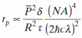
5.4 (a) A gold-coated microchain. (b) A structure made of a square of methacrylic polymer (left) and a square of acrylic polymer (right) that has been subjected to a copper metallization process. The acrylic polymer is coated selectively, while the methacrylic polymer remains pristine. (both reprinted with permission from Farrer et al., 2006)
If conformal coatings are desired, vapor-phase methods are also suitable for the coating of 3D polymeric structures created with MAP. Beyond simple evaporation or sputtering for deposition of metals, structures can be coated with a wide variety of materials using techniques such as chemical vapor deposition (Rill et al., 2008) and atomic layer deposition (Graugnard et al., 2009; King et al., 2006; Langner et al., 2008).
Inversion
For many applications in photonics, coatings are not sufficient to achieve the desired optical properties, such as refractive index contrast. In this case, 3D polymeric structures can be backfilled with other materials. If the voids in the 3D structure are on the scale of hundreds of nanometers, solution-phase approaches are not suitable for backfilling. Instead, techniques such as atomic layer deposition must be used to accomplish uniform filling.
Once backfilling has been achieved, the polymer is often removed by calcination. In this case, the backfilled material occupies the negative space of the original structure, and so the process as a whole is known as ‘inversion’ (King et al., 2006; Langner et al., 2008). It is also possible to backfill the inverted structure with a third material, and then to etch away the original backfilling material. This ‘double inversion’ process creates a structure with essentially the same geometry as the original polymeric structure but composed of an entirely different material (Tetreault et al., 2006).
Molding
Another approach to creating 3D structures from a wider range of materials is to use a polymeric structure fabricated with MAP to create a mold (LaFratta et al., 2004, 2006a). Molds are generally created with an elastomeric material such as polydimethylsiloxane (PDMS). The 3D structure is immersed in the elastomer, which is then allowed to set. The elastomeric mold is then removed from the master structure, and can be filled with a molding material and pressed against a substrate to create a replica. This technique is known as microtransfer molding (μTM). Each master structure can be used to create many molds, and each mold can be used to create many replicas (Fig. 5.5).
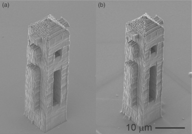
5.5 (a) Master structure created with MAP (b) Replica of the structure created with microtransfer molding. (both reprinted with permission from LaFratta et al., 2004)
The geometries of the master structures that can be used for μTM are limited due to the constraint that the mold must be able to be removed from the master structure (and from each replica). However, due to the elastic nature of PDMS, the topological constraints are not nearly as stringent as might be imagined (LaFratta et al., 2004). Additionally, a technique called membrane-assisted μTM (Fig. 5.6) even allows replicas with closed loops to be created (LaFratta et al., 2006a).
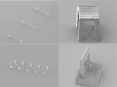
5.6 Examples of molded structures created with membrane-assisted microtransfer molding. (reprinted with permission from LaFratta et al., 2006a)
5.4 Applications of multiphoton lithography in photonics
Due to its ability to create high-precision, 3D nano- and micro-structures, applications of multiphoton fabrication have grown exponentially over the past decade. Here we will discuss examples of some of the prominent applications of multiphoton fabrication in photonics.
5.4.1 Micro-optics
The fabrication of micro-optics, such as lenses, phase plates and Fresnel optics, is often challenging using conventional lithography. Because these structures are three-dimensional, a gray-scale technique must typically be used for their fabrication on microscopic scales. Multiphoton fabrication is suited ideally for the rapid prototyping and production of 3D micro-optics. A number of groups have reported work in this area (Guo et al., 2006; Malinauskas et al., 2010a, 2010b; Yan et al., 2010), and multiphoton fabrication is a highly promising technique for creating both individual microoptics and arrays of micro-optics. Many of these devices are also amenable to molding after fabrication, making mass production feasible.
Multiphoton metal deposition has also been used to create micro-optics, such as diffraction gratings (Baldacchini et al., 2005; Cao et al., 2009; Kaneko et al., 2003b). By using multiphoton absorption to pattern helical channels in a positive-tone photoresist and then back-filling these channels with gold via electrodeposition, the creation of broadband circular polarizers has also been demonstrated (Gansel et al., 2009). This approach shows great promise for further applications in metamaterials.
It is also possible to incorporate dye molecules into structures created with MAP as a route to active micro-optics (Farsari et al., 2008; Sun et al., 2001; Yokoyama et al., 2003). The challenge with this approach is that the multiphoton polymerization process destroys many of the different molecules that it would be desirable to be able to incorporate. However, devices such as micro-scale, distributed-feedback lasers (Yokoyama et al., 2003) and dye-doped photonic crystals (Farsari et al., 2008) have been reported.
5.4.2 Waveguide-based devices
Because it can be used to create extremely smooth structures with feature sizes of a micrometre or less, multiphoton fabrication is well suited for the creation of waveguide-based devices. Multiphoton fabrication offers some advantages over other techniques for creating polymeric and dielectric-loaded waveguides, particularly in its ability to take advantage of the third dimension. The ability to incorporate other materials in or on fabricated structures may also provide a path towards making active devices and sensors.
In some of the first work on the creation of waveguides with MAP, devices such as couplers and interferometers were demonstrated between the ends of optical fibers (Klein et al., 2005, 2006). More recently, high-performance microring resonators (Fig. 5.7) have been demonstrated (Li et al., 2008a), in addition to index-modulated gratings within waveguides (Dong et al., 2007). Dielectric-loaded waveguides based on plasmonic metals are beginning to be explored as well (Reinhardt et al., 2009, 2010).

5.7 (a) Microring resonator created using MAP (b) Typical data from the through port of a microring resonator. (both reprinted with permission from Li et al., 2008a)
One of the attractive features of the 3D capability of multiphoton fabrication for waveguide devices is that it can be used for coupling of fibers with one another or with waveguides and on-chip photonic devices. 3D couplers or on-fiber optics can reduce coupling losses in optical systems considerably. As a result, interest is growing in the multiphoton fabrication of structures directly on the ends of optical fibers (Cojoc et al., 2010; Liberale et al., 2010) or on side-polished fibers (Sherwood et al., 2005).
5.4.3 Photonic crystals
Given the capability of multiphoton fabrication to create 3D structures with nanoscale resolution, its most popular application in optics has been in the creation of photonic crystals (Borisov et al., 1998; Deubel et al., 2004; Guo et al., 2005; Jia et al., 2009; Kaneko et al., 2003a, Sakellari et al., 2010; Serbin and Gu, 2006; Serbin et al., 2003; Straub et al., 2005; Sun et al., 1999). MAP is well suited for the creation of photonic crystals with nearly arbitrarily complex geometries, with resolution and voxel asymmetry being the main limitations in determining the geometries and operational wavelengths that can be achieved. Furthermore, because MAP is a direct-write method, defects such as cavities and waveguides can be created wherever desired within a photonic crystal.
MAP does have some drawbacks for the creation of photonic crystals. First, because it is a point-by-point fabrication method, the ultimate size of the photonic crystals that can be fabricated is typically on the order of hundreds of micrometres on a side. Photonic crystal structures are complex and have large numbers of voids, which means that they are not compatible with molding techniques. Second, material shrinkage upon exposure and development can distort photonic crystal structures, although this effect can generally be pre-compensated during fabrication. Finally, the index contrast between polymers and air is not sufficient to create a stop band. This last issue has been a major driver of research into the development of hybrid materials with higher refractive indices (Farsari et al., 2010; Sakellari et al., 2010; Serbin et al., 2003) and of inversion schemes (King et al., 2006; Langner et al., 2008; Tetreault et al., 2006).
5.4.4 Optical data storage
Another well-studied application of multiphoton absorption in photonics is in high-density optical data storage (Fig. 5.8) (Adam et al., 2010; Cumpston et al., 1999; Dvornikov et al., 2009; Iliopoulos et al., 2010; Li et al., 2008b; Olson et al., 2002; Wang and Stucky, 2004; Walker et al., 2008; Yanez et al., 2009b; Zhang et al., 2009). Rather than depositing material, in these approaches to optical memory multiphoton absorption is typically used to create a photochemical or photophysical change within a small volume of a macroscopic substrate. This change must later be able to be read out optically, either with a multiphoton process or, often preferably, with a linear process. Data are typically written in a binary format, and multiphoton absorption allows many layers to be addressed individually. Storage of a terabyte of data in 200 layers of a disk the size of a DVD has been demonstrated recently (Dvornikov et al., 2009; Walker et al., 2008). The key to practical commercial success for such devices will be achieving inexpensive and reliable read-out.

5.8 Data written in different planes of a molecular glass using multiphoton absorption. (reprinted with permission from Olson et al., 2002)
5.5 Future prospects for multiphoton lithography in photonics
Multiphoton fabrication offers unique capabilities for the creation of high-resolution, 3D structures, and can be performed with a table-top instrument. This technique is being used increasingly for applications in photonics. While multiphoton lithography is now a relatively mature technique, significant enhancements continue to be made both in materials and instrumentation. We can expect the resolution of this technique and the range of materials that can be employed to continue to improve in the coming years, enabling further applications and enhanced performance in photonics. Multiphoton fabrication is suited ideally to the prototyping of photonic devices as well as to the creation of devices for research purposes. If methods can be developed to increase the scalability of this technique, it has the potential to become a mainstay in the mass production of micro-and nano-photonic devices.
5.6 References
Adam, V., Mizuno, H., Grichine, A., Hotta, J.I., Yamagata, Y., Moeyaert, B., Nienhaus, G.U., Miyawaki, A., Bourgeois, D., Hofkens, J. Data storage based on photochromic and photoconvertible fluorescent proteins. Journal of Biotechnology. 2010; 149:289–298.
Baldacchini, T., Lafratta, C.N., Farrer, R.A., Teich, M.C., Saleh, B.E.A., Naughton, M.J., Fourkas, J.T. Acrylic-based resin with favorable properties for three-dimensional two-photon polymerisation. Journal of Applied Physics. 2004; 95:6072–6076.
Baldacchini, T., Pons, A.C., Pons, J., Lafratta, C.N., Fourkas, J.T., Sun, Y., Naughton, M.J. Multiphoton laser direct writing of two-dimensional silver structures. Optics Express. 2005; 13:1275–1280.
Bhuian, B., Winfield, R.J., O’Brien, S., Crean, G.M. Investigation of the two-photon polymerisation of a Zr-based inorganic-organic hybrid material system. Applied Surface Science. 2006; 252:4845–4849.
Borisov, R.A., Dorojkina, G.N., Koroteev, N.I., Kozenkov, V.M., Magnitskii, S.A., Malakhov, D.V., Tarasishin, A.V., Zheltikov, A.M. Fabrication of three-dimensional periodic microstructures by means of two-photon polymerisation. Applied Physics B: Lasers and Optics. 1998; 67:765–767.
Cao, Y.Y., Takeyasu, N., Tanaka, T., Duan, X.M., Kawata, S. 3D metallic nanostructure fabrication by surfactant-assisted multiphoton-induced reduction. Small. 2009; 5:1144–1148.
Chen, Y.S., Tal, A., Torrance, D.B., Kuebler, S.M. Fabrication and characterization of three-dimensional silver-coated polymeric microstructures. Advanced Functional Materials. 2006; 16:1739–1744.
Cojoc, G., Liberale, C., Candeloro, P., Gentile, F., Das, G., De Angelis, F., Di Fabrizio, E. Optical micro-structures fabricated on top of optical fibers by means of two-photon photopolymerisation. Microelectronic Engineering. 2010; 87:876–879.
Cumpston, B.H., Ananthavel, S.P., Barlow, S., Dyer, D.L., Ehrlich, J.E., Erskine, L.L., Heikal, A.A., Kuebler, S.M., Lee, I.Y.S., McCord-Maughon, D., Qin, J., Rockel, H., Rumi, M., Wu, X.-L., Marder, S.R., Perry, J.W. Two-photon polymerisation initiators for three-dimensional optical data storage and microfabrication. Nature. 1999; 398:51–54.
Denk, W., Strickler, J.H., Webb, W.W. Two-photon laser scanning fluorescence microscopy. Science. 1990; 248:73–76.
Deubel, M., Von Freymann, G., Wegener, M., Pereira, S., Busch, K., Soukoulis, C.M. Direct laser writing of three-dimensional photonic-crystal templates for telecommunications. Nature Materials. 2004; 3:444–447.
Dong, Y., Yu, X.Q., Sun, Y.M., Hou, X.Y., Li, Y.F., Zhang, M. Refractive index-modulated grating in two-mode planar polymeric waveguide produced by two-photon polymerisation. Polymers for Advanced Technologies. 2007; 18:519–521.
Dvornikov, A.S., Walker, E.P., Rentzepis, P.M. Two-photon three-dimensional optical storage memory. Journal of Physical Chemistry A. 2009; 113:13633–13644.
Farrer, R.A., Lafratta, C.N., Li, L., Praino, J., Naughton, M.J., Saleh, B.E.A., Teich, M.C., Fourkas, J.T. Selective functionalization of 3-D polymer microstructures. Journal of the American Chemical Society. 2006; 128:1796–1797.
Farsari, M., Ovsianikov, A., Vamvakaki, M., Sakellari, I., Gray, D., Chichkov, B.N., Fotakis, C. Fabrication of three-dimensional photonic crystal structures containing an active nonlinear optical chromophore. Applied Physics A: Materials Science & Processing. 2008; 93:11–15.
Farsari, M., Vamvakaki, M., Chichkov, B.N. Multiphoton polymerization of hybrid materials. Journal of Optics. 2010; 12:124001.
Fischer, J., Von Freymann, G., Wegener, M. The materials challenge in diffraction-unlimited direct-laser-writing optical lithography. Advanced Materials. 2010; 22:3578–3582.
Formanek, F., Takeyasu, N., Tanaka, T., Chiyoda, K., Ishikawa, A., Kawata, S. Three-dimensional fabrication of metallic nanostructures over large areas by two-photon polymerisation. Optics Express. 2006; 14:800–809.
Fourkas, J.T. Nanoscale photolithography with visible light. Journal of Physical Chemistry Letters. 2010; 1:1221–1227.
Gansel, J.K., Thiel, M., Rill, M.S., Decker, M., Bade, K., Saile, V., Von Freymann, G., Linden, S., Wegener, M. Gold helix photonic metamaterial as broadband circular polarizer. Science. 2009; 325:1513–1515.
Graugnard, E., Roche, O.M., Dunham, S.N., King, J.S., Sharp, D.N., Denning, R.G., Turberfield, A.J., Summers, C.J. Replicated photonic crystals by atomic layer deposition within holographically defined polymer templates. Applied Physics Letters. 2009; 94:263109.
Guo, R., Li, Z., Jiang, Z., Yuan, D., Huang, W., Xia, A. Log-pile photonic crystal fabricated by two-photon photopolymerisation. Journal of Optics A: Pure and Applied Optics. 2005; 7:396–399.
Guo, R., Xiao, S.Z., Zhai, X.M., Li, J.W., Xia, A.D., Huang, W.H. Micro lens fabrication by means of femtosecond two photon photopolymerisation. Optics Express. 2006; 14:810–816.
Haske, W., Chen, V.W., Hales, J.M., Dong, W.T., Barlow, S., Marder, S.R., Perry, J.W. 65 nm feature sizes using visible wavelength 3-D multiphoton lithography. Optics Express. 2007; 15:3426–3436.
Houbertz, R., Frohlich, L., Popall, M., Streppel, U., Dannberg, P., Brauer, A., Serbin, J., Chichkov, B.N. Inorganic-organic hybrid polymers for information technology: From planar technology to 3D nanostructures. Advanced Engineering Materials. 2003; 5:551–555.
Iliopoulos, K., Krupka, O., Gindre, D., Salle, M. Reversible two-photon optical data storage in coumarin-based copolymers. Journal of the American Chemical Society. 2010; 132:14343–14345.
Ishikawa, A., Tanakaa, T., Kawata, S. Improvement in the reduction of silver Ions in aqueous solution using two-photon sensitive dye. Applied Physics Letters. 2006; 89:113102.
Jia, B.H., Kang, H., Li, J.F., Gu, M. Use of radially polarized beams in three-dimensional photonic crystal fabrication with the two-photon polymerisation method. Optics Letters. 2009; 34:1918–1920.
Jun, Y., Leatherdale, C.A., Norris, D.J. Tailoring air defects in self-assembled photonic bandgap crystals. Advanced Materials. 2005; 17:1908–1911.
Kaneko, K., Sun, H.-B., Duan, X.-M., Kawata, S. Submicron diamond-lattice photonic crystals produced by two-photon laser nanofabrication. Applied Physics Letters. 2003; 83:2091–2093.
Kaneko, K., Sun, H.-B., Duan, X.-M., Kawata, S. Two-photon photoreduction of metallic nanoparticle gratings in a polymer matrix. Applied Physics Letters. 2003; 83:1426–1428.
King, J.S., Graugnard, E., Roche, O.M., Sharp, D.N., Scrimgeour, J., Denning, R.G., Turberfield, A.J., Summers, C.J. Infiltration and inversion of holographically defined polymer photonic crystal templates by atomic layer deposition. Advanced Materials. 2006; 18:1561–1565.
Klein, S., Barsella, A., Leblond, H., Bulou, H., Fort, A., Andraud, C., Lemercier, G., Mulatier, J.C., Dorkenoo, K. One-step waveguide and optical circuit writing in photopolymerizable materials processed by two-photon absorption. Applied Physics Letters. 2005; 86:211118.
Klein, S., Barsella, A., Taupier, G., Stortz, V., Fort, A., Dorkenoo, K.D. Optical components based on two-photon absorption process in functionalized polymers. Applied Surface Science. 2006; 252:4919–4922.
Kuebler, S.M., Rumi, M., Watanabe, T., Braun, K., Cumpston, B.H., Heikal, A.A., Erskine, L.L., Thayumanavan, S., Barlow, S., Marder, S.R., Perry, J.W. Optimizing two-photon initiators and exposure conditions for three-dimensional lithographic microfabrication. Journal of Photopolymer Science and Technology. 2001; 14:657–668.
Kumi, G., Yanez, C.O., Belfield, K.D., Fourkas, J.T. High-speed multiphoton absorption polymerisation: fabrication of microfluidic channels with arbitrary cross-sections and high aspect ratios. Lab on a Chip. 2010; 10:1057–1060.
Lafratta, C.N., Baldacchini, T., Farrer, R.A., Fourkas, J.T., Teich, M.C., Saleh, B.E.A., Naughton, M.J. Replication of two-photon-polymerized structures with extremely high aspect ratios and large overhangs. Journal of Physical Chemistry B. 2004; 108:11256–11258.
Lafratta, C.N., Fourkas, J.T., Baldacchini, T., Farrer, R.A. Multiphoton fabrication. Angewandte Chemie International Edition. 2007; 46:6238–6258.
Lafratta, C.N., Li, L., Fourkas, J.T. Soft-lithographic replication of 3D microstructures with closed loops. Proceedings of the National Academy of Sciences USA. 2006; 103:8589–8594.
Lafratta, C.N., Lim, D., O’Malley, K., Baldacchini, T., Fourkas, J.T. Direct laser patterning of conductive wires on three-dimensional polymeric microstructures. Chemistry of Materials. 2006; 18:2038–2042.
Langner, A., Knez, M., Müller, F., Gösele, U. TiO2 microstructures by inversion of macroporous silicon using atomic layer deposition. Applied Physics A: Materials Science & Processing. 2008; 93:399–403.
Li, L., Gattass, R.R., Gershgoren, E., Hwang, H., Fourkas, J.T. Achieving λ/20 resolution by one-color initiation and deactivation of polymerisation. Science. 2009; 324:910–913.
Li, L., Gershgoren, E., Kumi, G., Chen, W.Y., Ho, P.T., Herman, W.N., Fourkas, J.T. High-performance microring resonators fabricated with multiphoton absorption polymerisation. Advanced Materials. 2008; 20:3668–3671.
Li, X.P., Chon, J.W.M., Gu, M. Confocal reflection readout thresholds in two-photon-induced optical recording. Applied Optics. 2008; 47:4707–4713.
Liberale, C., Cojoc, G., Candeloro, P., Das, G., Gentile, F., De Angelis, F., Di Fabrizio, E. Micro-optics fabrication on top of optical fibers using two-photon lithography. IEEE Photonics Technology Letters. 2010; 22:474–476.
Malinauskas, M., Gilbergs, H., Žukauskas, A., Purlys, V., Paipulas, D., Gadonas, R. A femtosecond laser-induced two-photon photopolymerisation technique for structuring microlenses. Journal of Optics. 2010; 12:035204.
Malinauskas, M., Žukauskas, A., Purlys, V., Belazaras, K., Momot, A., Paipulas, D., Gadonas, R., Piskarskas, A., Gilbergs, H., Gaidukeviit, A., Sakellari, I., Farsari, M., Juodkazis, S. Femtosecond laser polymerisation of hybrid/integrated micro-optical elements and their characterization. Journal of Optics. 2010; 12:124010.
Maruo, S., Fourkas, J.T. Recent progress in multiphoton microfabrication. Laser & Photonics Reviews. 2008; 2:100–111.
Maruo, S., Saeki, T. Femtosecond laser direct writing of metallic microstructures by photoreduction of silver nitrate in a polymer matrix. Optics Express. 2008; 16:1174–1179.
Nagpal, P., Han, S.E., Stein, A., Norris, D.J. Efficient low-temperature thermo-photovoltaic emitters from metallic photonic crystals. Nano Letters. 2008; 8:3238–3243.
Olson, C.E., Previte, M.J.R., Fourkas, J.T. Efficient and robust multiphoton data storage in molecular glasses and highly crosslinked polymers. Nature Materials. 2002; 1:225–228.
Reinhardt, C., Seidel, A., Evlyukhin, A.B., Cheng, W., Chichkov, B.N. Mode-selective excitation of laser-written dielectric-loaded surface plasmon polariton waveguides. Applied Physics B: Lasers and Optics. 2009; 26:B55–B60.
Reinhardt, C., Seidel, A., Evlyukhin, A., Cheng, W., Kiyan, R., Chichkov, B. Direct laser-writing of dielectric-loaded surface plasmon-polariton waveguides for the visible and near infrared. Applied Physics A: Materials Science & Processing. 2010; 100:347–352.
Rill, M.S., Plet, C., Thiel, M., Staude, I., Von Freymann, G., Linden, S., Wegener, M. Photonic metamaterials by direct laser writing and silver chemical vapour deposition. Nature Materials. 2008; 7:543–546.
Sakellari, I., Gaidukeviciute, A., Giakoumaki, A., Gray, D., Fotakis, C., Farsari, M., Vamvakaki, M., Reinhardt, C., Ovsianikov, A., Chichkov, B.N. Two-photon polymerisation of titanium-containing sol-gel composites for three-dimensional structure fabrication. Applied Physics A: Materials Science & Processing. 2010; 100:359–364.
Serbin, J., Gu, M. Experimental evidence for superprism effects in three-dimensional polymer photonic crystals. Advanced Materials. 2006; 18:221–224.
Serbin, J., Egbert, A., Ostendorf, A., Chichkov, B.N., Houbertz, R., Domann, G., Schulz, J., Cronauer, C., Frohlich, L., Popall, M. Femtosecond laser-induced two-photon polymerisation of inorganic-organic hybrid materials for applications in photonics. Optics Letters. 2003; 28:301–303.
Sherwood, T., Young, A.C., Takayesu, J., Jen, A.K.Y., Dalton, L.R., Antao, C. Microring resonators on side-polished optical fiber. IEEE Photonics Technology Letters. 2005; 17:2107–2109.
Stellacci, F., Bauer, C.A., Meyer-Friedrichsen, T., Wenseleers, W., Alain, V., Kuebler, S.M., Pond, S.J.K., Zhang, Y.D., Marder, S.R., Perry, J.W. Laser and electron-beam induced growth of nanoparticles for 2D and 3D metal patterning. Advanced Materials. 2002; 14:194–198.
Stocker, M.P., Li, L., Gattass, R.R., Fourkas, J.T. Multiphoton photoresists giving nanoscale resolution that is inversely dependent on exposure time. Nature Chemistry. 2011; 3:225–229.
Straub, M., Nguyen, L.H., Fazlic, A., Gu, M. Complex-shaped three-dimensional microstructures and photonic crystals generated in a polysiloxane polymer by two-photon microstereolithography. Optical Materials. 2005; 27:359–364.
Sun, H.-B., Matsuo, S., Misawa, H. Three-dimensional photonic crystal structures achieved with two-photon-absorption photopolymerisation of resin. Applied Physics Letters. 1999; 74:786–788.
Sun, H.-B., Tanaka, T., Takada, K., Kawata, S. Two-photon photopolymerisation and diagnosis of three-dimensional microstructures containing fluorescent dyes. Applied Physics Letters. 2001; 79:1411–1413.
Tan, D., Li, Y., Qi, F., Yang, H., Gong, Q., Dong, X., Duan, X. Reduction in feature size of two-photon polymerisation using SCR500. Applied Physics Letters. 2007; 90:071106.
Tanaka, T., Ishikawa, A., Kawata, S. Two-photon-induced reduction of metal ions for fabricating three-dimensional electrically conductive metallic microstructure. Applied Physics Letters. 88, 2006. [081107/1–081107/3].
Tetreault, N., Von Freymann, G., Deubel, M., Hermatschweiler, M., Perez-Willard, F., John, S., Wegener, M., Ozin, G.A. New route to three-dimensional photonic bandgap materials: Silicon double inversion of polymer templates. Advanced Materials. 2006; 18:457–460.
Tosa, N., Vitrant, G., Baldeck, P.L., Stephan, O., Astilean, S., Grosu, I. Two-photon laser deposition of gold nanowires. Journal of Optoelectronics and Advanced Materials. 2007; 9:641–645.
Tosa, N., Vitrant, G., Baldeck, P.L., Stephan, O., Grosu, I. Fabrication of 3D metallic micro/nanostructures by two-photon absorption. Journal of Optoelectronics and Advanced Materials. 2008; 10:2199–2204.
Vurth, L., Baldeck, P., Stephan, O., Vitrant, G. Two-photon induced fabrication of gold microstructures in polystyrene sulfonate thin films using a ruthenium(II) dye as photoinitiator. Applied Physics Letters. 2008; 92:171103.
Walker, E., Dvornikov, A., Coblentz, K., Rentzepis, P. Terabyte recorded in two-photon 3D disk. Applied Optics. 2008; 47:4133–4139.
Wang, J., Stucky, G.D. Mesostructured composite materials for multibit-persite optical data storage. Advanced Functional Materials. 2004; 14:409–415.
Witzgall, G., Vrijen, R., Yablonovitch, E., Doan, V., Schwartz, B.J. Single-shot two-photon exposure of commercial photoresist for the production of three-dimensional structures. Optics Letters. 1998; 23:1745–1747.
Wong, S., Deubel, M., Perez-Willard, F., John, S., Ozin, G.A., Wegener, M., Von Freymann, G. Direct laser writing of three-dimensional photonic crystals with complete a photonic bandgap in chalcogenide glasses. Advanced Materials. 2006; 18:265–269.
Xing, J.-F., Dong, X.-Z., Chen, W.-Q., Duan, X.-M., Takeyasu, N., Tanaka, T., Kawata, S. Improving spatial resolution of two-photon microfabrication by using photoinitiator with high initiating efficiency. Applied Physics Letters. 2007; 90:131106.
Yan, L., Yu, Y., Guo, L., Wu, S., Chen, C., Niu, L., Li, A., Yang, H. High efficiency multilevel phase-type Fresnel zone plates produced by two-photon polymerisation of SU-8. Journal of Optics. 2010; 12:035203.
Yanez, C.O., Andrade, C.D., Belfield, K.D. Characterization of novel sulfonium photoacid generators and their microwave-assisted synthesis. Chemical Communications. 2009; 7:827–829.
Yanez, C.O., Andrade, C.D., Yao, S., Luchita, G., Bondar, M.V., Belfield, K.D. Photosensitive polymeric materials for two-photon 3D WORM optical data storage systems. ACS Applied Materials & Interfaces. 2009; 1:2219–2229.
Yang, D., Jhaveri, S.J., Ober, C.K. Three-dimensional microfabrication by two-photon lithography. MRS Bulletin. 2005; 30:976–982.
Yokoyama, S., Nakahama, T., Miki, H., Mashiko, S. Fabrication of three-dimensional microstructure in optical-gain medium using two-photon-induced photopolymerisation technique. Thin Solid Films. 2003; 438–439:452–456.
Yu, T., Ober, C.K., Kuebler, S.M., Zhou, W., Marder, S.R., Perry, J.W. Chemically amplified positive resists for two-photon three-dimensional microfabrication. Advanced Materials. 2003; 15:517–521.
Zhang, Z.S., Hu, Y.L., Luo, Y.H., Zhang, Q.J., Huang, W.H., Zou, G. Polarization storage by two-photon-induced anisotropy in bisazobenzene copolymer film. Optics Communications. 2009; 282:3282–3285.
Zhou, W., Kuebler, S.M., Braun, K.L., Yu, T., Cammack, J.K., Ober, C.K., Perry, J.W., Marder, S.R. An efficient two-photon-generated photoacid applied to positive-tone 3D microfabrication. Science. 2002; 296:1106–1109.