
Laser growth and processing of photonic structures: an overview of fundamentals, interaction phenomena and operations
Abstract:
Laser materials processing meets some innovative applications for advanced photonic technologies. The use of lasers in the fabrication of unique devices unavailable by other means opens up a field rich of science and engineering and promises many benefits in the years to come. This chapter illustrates the fundamental effects and the concepts behind the applications addressed in this book. It overviews the phenomena and the underlying mechanisms and sets the basis for understanding the advanced topics discussed in the following chapters. It further continues with a more detailed presentation of laser ablation methods in materials growth and processing. This part concludes summarizing the trends and prospects of emerging laser-based technologies in the fabrication of photonics devices.
1.1 Laser processing concepts and processes: an introduction
Laser radiation emerged in the 1960s as a very promising alternative tool in materials science and technology (Beesley, 1978). Novel sources of coherent radiation had the ability to provide a large amount of directional energy which could be handled and manipulated in free space with remarkable convenience using optical systems. Significant advantages are drawn from the high intensity, directionality and wavelength specificity of radiation. Radiation energy can thus be efficiently coupled into the workpiece and results in spatial localization of laser–matter interactions, enabling the achievement of superior quality processing results and providing novel means for advanced materials processing and engineering (Ion, 2005).
Primarily addressing cutting and welding in the engineering workshop, this technology progressed steadily to several industrial applications, from the heavy shipbuilding industry to the niche micro-engineering foundry (Steen and Mazumder, 2010). The growth of photonic materials, the fabrication of novel optical systems and the tailoring of complex waveguiding circuits are some first steps addressed in this book aiming at the realization of the future miniaturized three-dimensional (3D) photonics and hybrid multifunctional nanosystems.
Initial applications of lasers in materials processing have mainly relied on thermal effects produced by the use of high power carbon dioxide (CO2) lasers. This most energy efficient laser source emits 10.6 μm radiation in the long wave infrared (IR) region. Its ability to deliver kilowatt power beams in both the continuous wave (CW) and pulsed emission modes, at considerably low capital and running costs, makes it a favoured choice for materials processing. Depending on the optical properties of materials, energy is effectively transferred from the laser beam to the workpiece and it is coupled into a rather small volume near the surface, resulting in the rapid localized increase of temperature in the interaction region. Thermal properties take up and become responsible for the evolution of consequent effects. In the 1970s materials cutting, drilling and welding, followed by surface processing, such as thermal annealing and alloying, were all successfully adopted by the industry (Cline and Anthony, 1977).
Laser material interactions are usually initiated by focused laser radiation. Depending on the rate of energy deposition and the energy out-diffusion from the interaction region to the bulk, a number of associated effects, from phase changing and melting to evaporation and ablation, are possible. The properties of the laser radiation and the nature of the material determine the highly interdependent physical and chemical effects which yield processing of the material (Bäuerle, 2000).
Thermal processing of a metallic sample irradiated by a laser beam is an excellent example to illustrate the range of operations:
(a) At low laser intensity heating at a suitably high temperature causes phase transformation and leads to the alteration of the mechanical, electrical, optical or other properties of the material.
(b) Increasing the energy deposition produces melting and consecutive resolidification in a spatially localized region. This may result in phase transformation while more intense effects of crystallization or amorphization and vitrification can be produced depending on the conditions. In this mode, alloying and impurity doping by in-diffusion are also possible yielding considerable structural modifications and improving materials performance.
(c) Higher laser intensities can produce local vaporization of the material and mass removal from the interaction region under thermodynamic equilibrium. This process can be quite slow at relatively low intensities. The resulting heat diffusion yields an extended re-solidification and heat affected zone. Materials vaporization and removal in this case becomes a distillation process yielding elemental separation and phase transformations.
(d) Using very high-intensity nanosecond pulses, the above vaporization process evolves rapidly under non-equilibrium conditions. The energy is deposited in such a very short time scale which effectively does not allow heat diffusion through the bulk. A small superheated volume is explosively vaporized. Violent materials ejection occurs usually associated with the production and evolution of plasma. This is the so-called pulsed laser ablation (PLA) process. It is associated with minimization of the heat-effected zone and the simultaneous congruent removal of the materials constituents, in a mixture of atoms and ions, molecules, clusters and micro-particulates.
Laser technology advanced very rapidly (Siegman, 1986). The advent of lasers emitting at shorter wavelengths offered novel potential for materials processing due to the high energy photons absorbed near the surface. In addition, the stronger focusing and higher resolution imaging at short wavelengths set the basis of the laser micro-processing technology. Original developments in the field concerned thermal processing by use of pulsed Nd:YAG lasers emitting from a few milli-joules to several joules per pulse at 1.06 μm in the near infrared (NIR). Such systems are currently deployed in industrial operations for laser welding, cutting and drilling achieving micron scale accuracy appropriate for the micro-engineering and micro-electronics industries. Solid state laser sources emitting higher harmonics, as for example 2ω:532 nm, 3ω:355 nm and 4ω:266 nm of the Nd:YAG, as well as metal-vapour high power lasers, offered new tools based on visible and ultraviolet (UV) wavelengths, improved the accuracy and enhanced the coupling of radiation with superior results.
Significant advances are recorded with the availability and deployment of excimer lasers emitting mid and deep-UV radiation in nanosecond duration pulses (Laude, 1994). The intense beams of highly energetic photons produced by the metastable dimmers (emitting at) XeCl (308 nm), KrF (248 nm), ArF (193 nm) and more recently, F2 (157 nm) lasers, are responsible for a number of distinct processing operations unavailable by other means. First, the absorption coefficient at these short wavelengths is large for most materials and this reduces significantly the penetration depth (defined to 1/e2 intensity point) of the incident radiation. The result is the accumulation of energy in a very shallow interaction volume near the irradiated surface of the sample. In effect, a considerable amount of energy is deposited typically in a few nanoseconds in a very limited material volume. The material becomes superheated and ablated. Second, the photon energy may be capable of direct molecular photo-dissociation, or can trigger violent photochemical reactions and photomechanical effects. Overall such effects yield superior processing quality with minimal thermally affected zones. Third, materials ablation is a congruent process as it produces highly energetic multi-component plasma owing to the minimization of the inter-action region, heat transport and loss through the bulk. The deposition of the ablated material on solid substrates opened up the field of pulsed laser deposition (PLD) we address here (Chrisey and Hubler, 1994).
The availability of intense UV laser sources made possible a number of indirect non-destructive processes primarily relating to photo-polymerization, which to date has proved of the utmost importance in microfabrication technologies (Jain, 1990). The operations take advantage of the narrow line-width spatially incoherent UV laser sources, to yield short exposure times and improved imaging and irradiation procedures. These features have enabled accurate processing methods in micro-fabrication production lines and they have been integrated as an efficient industrial standard technology for micro-engineering, micro-electronics and photonics. Further photophysical and reactive photochemical processing methods for surface treatment and laser-assisted vapour deposition by use of precursor compounds for applications in micro-engineering, aerospace and other niche areas have been exhaustively investigated (Bäuerle, 2000). Direct ablative processing also attracts great interest as a viable alternative to conventional multi-step lithographic methods. The method has been developed and applied as a single step processing tool for micro-optics and multifunction device fabrication exhibiting great flexibility and universality as discussed in this work.
In recent years ultra-short laser pulses became available, with the Ti:sapphire laser system attracting major interest, due to its capability to emit sub-picosecond pulses, from about 200 femtoseconds, to less than 50 fs at 800 nm. Pulse energies range from the nJ/pulse produced by the high repetition rate (100 MHz) oscillators, to mJ/pulse low repetition rate main frame amplifier systems yielding from GW to TW range peak intensities. In this range the absorption of materials reaches the nonlinear regime. Materials transparent at the irradiating wavelength are becoming opaque due to nonlinear absorption with severe consequences in their response.
Ultra-short pulsed laser radiation defines the current research trends in laser materials processing and fabrication (Haglund, 2006). Although several well-established operations employing IR and UV lasers represent today’s industrial standards, multiphoton processing offers new potential and unique advantages. Multiphoton absorption reflects on further localization of the deposited energy in the high-intensity region of the beam. This is also assisted by the high quality Gaussian beams produced, which allow efficient beam control and delivery to the target workpiece. High quality direct ablative and/or photophysical and photochemical reactive processing are obtained.
This chapter provides an overview of the fundamental concepts and laser interaction effects, emphasizing mechanisms and parameters in the context of materials growth and processing. It aims to establish the appropriate background and guide the reader through the main body of this book. Acquaintance with the underlying basic physics and optics is assumed. Emphasis is placed on the physical notions of the various processes, rather than a complete mathematical treatment of the various quite complex topics, most of which are subjects of current research.
The growth and processing of photonic materials adds a new dimension to the traditional laser materials processing technology, owing to further stringent requirements imposed by the optical quality and the special properties of the final product. Pointing to the important aspects and parameters involved, the second section of this chapter summarizes the concepts behind the real processing systems and includes aspects of laser beam propagation and radiation coupling. A more detailed overview of the fundamental processes is found in section three, commencing from the absorption of radiation and elaborating the energy coupling and macroscopic processing effects. The fourth section aims to introduce the most important materials processing operations for photonics, focusing on cases of ablative operations and device fabrication. The final section concludes the discussion by summarizing the trends of this emerging technology and gives the floor to the eminent contributors of this book.
1.2 Laser radiation, propagation and delivery
1.2.1 Laser radiation, properties and sources
Laser radiation today covers an extended section of the electromagnetic spectrum, from the deep-UV to the far-infrared (FIR), while free electron systems extend to the X-ray region. CW and pulsed laser systems are available, delivering from a few mW to several kW optical power and laser pulses of millisecond to femtosecond duration at pulse energy levels ranging from nJ to several Joules for industrial systems, or kJ for systems developed for fusion and other high energy applications.
The principal properties of laser radiation, as contrasted to incoherent radiation in the same spectral regions, are briefly outlined here:
(a) The coherence of laser radiation is the result of the stimulated emission process in the atomic or molecular system. It relates to the narrow spectral bandwidth into which all available energy is channelled, thus achieving a very high spectral density. In addition to the tremendous properties of interference and diffraction, this property allows a wide range of applications including spectral pumping and tuning, efficient nonlinear propagation, selective absorption and activation and others.
(b) The directionality of the radiation by the formation of Gaussian beams is the result of the optical resonance necessary to achieve and sustain laser oscillation. Laser beams have increased spatial coherence and exhibit minimal deterioration due to diffraction, thus enabling efficient energy transmission and delivery on the target under processing.
(c) Both the above aspects are responsible for the celebrated high intensity of the laser beam, which together with the spatial and temporal coherence, as well as the polarization control, are crucial in materials processing operations.
A limited number of laser types have been proved suitable for and are efficiently deployed in materials processing. While laser radiation covers a very broad spectrum, from the X-ray or deep-UV to the FIR region, a number of significant appropriate parameters and requirements must be fulfilled, including:
(i) Wavelength of radiation, propagation in free space and absorption by the workpiece under processing. Selection of specific wavelength is important in many cases. It determines the beam delivery technology and the nature of operations.
(ii) Emission at CW and/or pulsed operation. It determines the nature and range of operations, as well as the technical and financial aspects of the deployed technology.
(iii) Efficiency of operation in technical and economic terms and power efficiency in reference to electrical-to-optical power conversion. It affects the operational costs and the market value of the final products.
(iv) Reliability of operation, technology complexity and automation. They are very important in the industrial floor.
(v) Acquisition and operational costs, production efficiency and final product price. They affect primarily the industrial production and also research operations.
The selection of laser types currently available and used in the materials processing operations includes:
(a) Carbon dioxide laser: CO2 laser emitting at 10.6 μm from the molecular transitions of carbon dioxide. Highly efficient (~ 30%) system offering both pulsed and CW operations from mW to kW CW output power levels and pulses of mJ to kJ energy. Systems widely deployed in industrial production, from heavy industry to microelectronics.
(b) Excimer lasers produce UV radiation by the metastable excited molecular dimers ArF (193 nm), KrF (248 nm), XeCl (308 nm) and the more recently developed F2(157 nm). They only emit pulsed operation and are pumped by high current discharges or electron beams. Their efficiency varies depending on their type. They deliver mJ to Joule pulses, of a few nanoseconds’ duration. Special hybrid dye-excimer systems offer sub-picosecond radiation. Excimer lasers offer highly energetic photons and enable unique operations, even though their beam coherence and spatial quality are reduced and limited by the electric discharge effects.
(c) Nd:YAG, Nd:Glass and related rare earth solid sate laser systems. Nd-based solid state sources have been and are widely used owing to their high efficiency operation at the NIR and the potential of visible and UV emission by use of frequency doubling and optical parametric oscillator systems. By these means they cover the range from the UV to the mid-IR, although at varying laser efficiencies. In addition to the fundamental frequency ω: 1064 nm, significant wavelengths deployed are 2ω: 532 nm, 3ω: 355 nm and 4ω: 266 nm. The use of various laser hosts and ions give new possibilities with prime candidates the Er+ (1.5–1.6 μm) and the Ho+ (2.1 μm) laser systems. Solid state technology has become widespread and enables highly efficient operations by the use of spectrally selective pumping by diode lasers. Systems deployed in CW at power levels of less than 1 mW to kW and pulsed modes emitting from the quasi CW to picoseconds pulses of nJ to tens of J energy are well established in industry. The wide range of free space systems is now enriched by the production of all-fibre lasers which deliver picosecond and femtosecond pulse trains in the NIR.
(d) Semiconductor diode lasers are deployed owing to the achievement of considerably high power levels delivered by laser diodes arrays. They operate in both pulsed and CW modes, achieving power levels approaching the 1 kW in the NIR range from ~ 800 nm to ~1600 nm. They are small, compact and reliable sources of very robust construction and in most cases offer fibre delivery alleviating the hazards of invisible radiation.
(e) Ti-Sapphire, Ti:Al2O3 laser system emitting broadband radiation at ~ 800 nm. This is one of the latest solid state laser developments which operate in the CW and pulsed modes. The broad gain bandwidth allows efficient mode locked operation producing 150 fs pulse trains at ~ 100 MHz repetition rates and above. By use of pulse compression and amplification techniques, these lasers offer currently sub-50 fs pulses of mJ energy, yielding extremely high peak power levels and several TW/cm2 intensities on target. These systems offer an extended wavelength selection by use of optical parametric oscillators (UV to NIR). Their use defines the current trends in several fields.
1.2.2 Laser beam formation and propagation
Optical feedback is fundamental in the operation of the laser oscillator. The optical cavity containing the active laser medium redirects the photons needed for stimulating the emission and thus determines the formation of the output laser beam. The feedback operation sets the boundaries for the propagation of the otherwise plane wave. It limits the spatial and temporal characteristics of the oscillating field by requiring a self-consistent regeneration of the optical field. The latter established in the resonator yields the specific spatial and spectral content of the emitted radiation.
The high intensity of the laser beam is the result of two effects. First, the stimulated emission is by nature a coherent process yielding high intensity and spectral purity. Second, the paraxial localization of propagating energy, with the formation of Gaussian beams in the laser cavity, limits the cross-sectional area and results in high intensities. Coherent laser radiation thus exhibits a narrow spectrum which can be tuned, filtered, modulated and generally manipulated in space and time.
Central to the laser oscillation is the formation of the fundamental Gaussian beam in the laser resonator (Yariv, 1986). It is the field mode determined by wave propagation under the slowly varying envelope approximation and represents the diffraction limited case. The beam reproduces itself in the resonator self-consistently and ‘survives’ after infinite round trips.
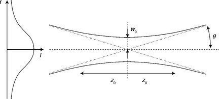
Figure 1.1 presents the typical geometry of the time-independent Gaussian beam propagating along the z-axis with wave vector, k, given by equation 1.1 as a function of various significant parameters defined in Table 1.1. The beam extends laterally to infinity. The spatial limits shown in Fig. 1.1 represent the envelope to 1/e points of the maximum electric field at z-position, or equivalently to 1/e2 intensity points, with respect to the on axis, z = 0, maximum value. The hyperboloid bounds physically the major part of the power transmitted along the z-direction.
Table 1.1
Notation and physical content of the fundamental Gaussian beam and related parameters
| 1 | W0 | Beam waist; the radius of the beam spot at focus; a measure of the diffraction limit. |
| 2 | w(Z) | Spot size; radius of the spot at the specified position z of the propagation axis. |
| 3 | q(z) | Complex radius of the beam at position z. |
| 4 | R(z) | Real radius of curvature of the wavefront at position z. |
| 5 | η(z) | Phase parameter describing the on axis departure of the wavefront from the phase of the planar wave. |
| 6 | Z0 | The distance from focus (z = 0) at which the cross-sectional area of the beam is doubled. Also referred as the Rayleigh length and defines the confocal parameter or depth-of-focus (DOF) of the beam, b = 2zo, the region in which the beam is considered to remain in focus. |
| 7 | θ0 | Divergence of the Gaussian beam; defines the diffraction limit and the speed of intensity decrease along propagation. |
| 8 | θM | Actual beam divergence. |
| 9 | M2 | M2-factor; determines the departure from the ideal Gaussian form; a measure of beam quality. |
Eq. [1.1] is an analytical expression of the fundamental Gaussian field:
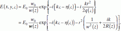
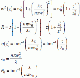
where the various significant parameters are defined in Eq. [1.2] and their significance is outlined in Table 1.1:
The spatial extent, w(z), of the beam determines the area of the interaction region, which is irradiated by the beam and it is a very important parameter as it defines the intensity, the power and the energy deposited on the target workpiece under processing.
Bearing in mind that in many processing operations focused radiation is used, the spot size at beam waist, w0, becomes of extreme importance and, effectively, determines the maximum intensity on target and the minimum interaction region. In turn, they reflect on the overall ‘intensity profile’ available to the processing operation which affects the results.
One important aspect of the Gaussian beam concerns its propagation properties. The Gaussian function transmitted in free space is responsible for the spatial invariability of its form. Diffraction in the far field (Fraunhofer region) is determined by Fourier transformations and preserve the Gaussian shape of the beam. In addition, transmission of the Gaussian field through an ideal lens becomes equivalent to the far-field diffraction and preserves the beam shape. It is important to underline here again the significance of the spot size, w0. The diffraction limited beam divergence, θ0, is inversely proportional to the ‘tightness’ of focus. A strongly focusing beam rapidly converges towards the focal point and then diverges fast on its propagation. The focusing condition determines the interaction volume and the intensity and energy content, which are the most crucial parameters for the processing operations. On the other hand, a weakly focused Gaussian beam having a small divergence is the most appropriate for radiation transmission and delivery, since it results in minimum energy loss through the system, while preserving the main beam characteristics, even in the presence of optical imperfections. Very important to the focusing and propagation properties is the confocal parameter of the beam. It is also referred to as the Rayleigh length, zo, and describes the depth-of-focus (DOF) of the beam. It is the ±z-point where spot size increases by 21/2 with respect to the waist, or equivalently, the spot area becomes doubled, thus representing the best focus region.
In the above context, the importance of a beam quality parameter M2-factor becomes apparent. A real laser beam usually departs from the ideal diffraction limited case, with the consequence of a larger beam divergence and confocal parameter (depth of focus) for a given spot size. The beam quality parameter, M2-factor, is defined by Eq. [1.3] in terms of actual beam divergence with respect to the ideal Gaussian as:

In addition to the fundamental Gaussian beam discussed above, higher order solutions-modes of the wave equation may exist under certain boundary values imposed by the resonator optics.
The larger spatial extent is also expressed in terms of the M2-factor. The possible coupling and power between modes, however, should also be mentioned and relates to the delivered laser beam quality on target. This is a crucial parameter affecting directly the final processing quality.
1.2.3 Laser beam delivery and radiation coupling
Laser power is delivered on target either directing the beam in free space using reflecting and focusing elements, such as lenses and mirrors, or by use of fibre optics including solid, hollow or liquid filled lightguides.
The Fourier transformations preserve the Gaussian form in free space propagation and delivery. In effect, natural diffraction transforms the Gaussian beam to itself, by effectively changing the pair (wo, θo), thus preserving the power but amending appropriately the intensity profile along the path. The optical system may take the form of a free space waveguide, formed by use of a series of focusing elements. This implies maximum transmission efficiency, experimentally approaching the diffraction limited performance. Various practical experimental geometries have been developed in the form of table-top optical systems, flat-bed and scanning work-stations, as well as robotic articulated-arm delivery systems.
The use of fibre optics and lightguiding offers significant advantages and convenience of operations covering the range from the deep-UV (> 200 nm) to the extended NIR (3 μm). Speciality silica fibres are used to transmit radiation of wavelength below 250 nm and non-oxide, chalcogenide glass (Ga-La-S, Ag-Se) waveguides transmit in the far-IR wavelengths above 5 μm. In cases requiring high power transmission, hollow and liquid filled light pipes are used, however, at decreased beam quality.
In materials processing operations, laser radiation must be optically coupled to the workpiece via its optical interphase, as depicted in Fig. 1.2. Figure 1.2a presents a typical laser beam, 1, incident on the target, 2. Irrespective of the specifics, the incident field may be approximated by a plane wave of wavelength, λ, and electric field, E, where:

1.2 (a) Specular reflection and transmission geometry by an ideal planar interphase with inset absorption graph and (b) reflection and diffraction by a real interphase exhibiting a finite roughness (drawn exaggerated for clarity). Incident beam (1), sample (2), reflected beam (3), transmitted/scattered and absorbed beams (4).
Part of the incident radiation is reflected in a specular mode, 3, and a part, 4, is transmitted and absorbed in the material (Born and Wolf, 1989).
In effect the material exhibits a complex refractive index:
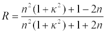
where n is the real part and k is the imaginary part describing energy loss. For a planar interface the reflection coefficient for normal incidence is given by:
Practically the beam transmitted in the z-axis is described by:
and undergoes absorption. The absorbed fraction of the incident power is used for processing the irradiated material. In the linear absorption regime the absorption coefficient, α, and penetration depth, δ (illustrated in Fig. 1.2), in a first approximation independent of the intensity, given by:
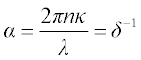
describe the exponential decay of the field along propagation into the bulk workpiece. These parameters are of great significance since, in conjunction with the spatial extent of the irradiating beam, they determine the laser–matter interaction volume.
Depending on the absorption coefficient, α, at the particular wavelength, penetration depth for the deep UV may be in the nanometre scale for many materials and certainly for metals. Figure 1.2b illustrates a more realistic situation. A laser beam approximated by the plane wave, 1, is incident on a nearly planar but textured sample, 2, having a finite roughness as met in most cases. A specularly reflected beam 3 is observed, but the inclusion of surface imperfections modifies significantly the problem. A scattered beam, 4, is observed at the interface and energy is redistributed with a part in free space and another part coupled into the material bulk.
(a) Irrespective of the nature of the material, the workpiece is described by a 3D interphase profile function of the form nc(x, y, z), which can be analysed in terms of spatial frequencies.
(b) The incident field is diffracted by this interphase in both semi-spaces breaking up into components determined by the particular geometrical and physical characteristics of the problem. The presence of suitable spatial frequencies in the sub-wavelength regime may reduce severely the reflectivity and can effectively produce opacity by presenting an artificial refractive index to the incident wave. Radiation may thus be coupled into the sample and become absorbed, irrespective of the prime natural reflection properties of the material. A totally different absorption response is therefore attained by the otherwise assumed ‘planar’ but textured interphase.
(c) The existence of localized imperfections produces scattering which leads to local modifications of the field. The ideal planar wave incident on the workpiece produce large local field intensities which can affect the material significantly. Multi-pulse irradiation produces localized damage in the material even at relatively low average intensity. Subsequent pulses may thus find totally different surface properties, which in nominal terms respond quite unexpectedly.
Further to the above, the use of ultra-short pulse high-intensity radiation yields nonlinear refraction and absorption effects. In practice this may be equivalent to the absorption at Ω = nω, but the relevant refractive index and absorption coefficients are functions of radiation intensity and the overall absorption along the propagation may be described by:

where the first is the linear term and the second and following terms with nonlinear absorption coefficients β,μ,…,ξ, respectively concern the possible 2-, 3-, … n-photon processes participating in the interaction with decreasing probabilities of occurrence.
Overall, the delivery of laser radiation and the coupling to the target is a complex problem which traditionally has been overlooked. Experimental evidence shows that the quality of the laser processing results depends primarily on surface properties which affect severely the radiation coupling. This may become of prime importance when working in the photonics miniaturization domain close to diffraction limits, where processing quality and accuracy at the microscopic level are important issues.
1.3 Summary of the interactions of laser radiation with condensed matter
The interactions of laser radiation with solid materials are primarily determined by the nature of the materials and the properties of the laser radiation, which define the parameter space of the individual problem. The high precision required in photonics and micro-engineering usually necessitates specific measures and advanced technological solutions. The requirements for each operation may differ significantly. Even though the basic technology remains the same, the high accuracy needed required our understanding of the fundamentals, in order to master the processing operations.
1.3.1 An outline of fundamental effects
The materials processing operations and observed phenomena are closely associated with a range of fundamental interactions:
(i) Electronic excitation and de-excitation upon radiation absorption: Transitions between bands by use of a single photon or many photons (multiphoton), associated with radiation emission (fluorescence, luminescence) and also non-radiative energy transfer via coupling to the lattice which may cause significant structural modifications.
(ii) Photo-ionization: Removal of electrons to the vacuum state usually followed by avalanche ionization, which leads to materials breakdown, triggering ablation and plasma formation.
(iii) Molecular photo-dissociation: Absorption and excitation to repulsive states leads to the dissociation of molecular bonds and disintegration of the material.
(iv) Photochemical reactions: Activation of chemical reactions, synthesis of new molecules or manipulation effects.
(v) Laser-plasma effects: formation, plasma post-ionization, resonant effects and superheating.
(vi) Other atomic and molecular interactions: radiation-induced forces, optical trapping and atomic cooling.
1.3.2 Range of macroscopic phenomena
Macroscopic phenomena observed are directly or indirectly associated with the above fundamental processes. They are supportive or detrimental to the materials processing operations. More specifically:
(a) Thermal effects are of prime interest and their participation cannot be excluded in any case. They range from the initial phase transformation to melting and re-solidification, evaporation and pyrolysis, processes evolving under thermodynamic equilibrium.
(b) Photomechanical effects relate to the direct or indirect application of mechanical forces. At low light intensities they concern radiation pressure and gradient field forces. In addition, thermomechanical stress effects, acoustic waves and shockwaves can be induced at high intensities, especially upon photo-ablation.
(c) Photochemical effects, including photo-dissociation and photolysis, photo-catalysis, photochemical reactions, photosynthesis and photopolymerization.
(d) Photo-desorption and photo-ejection from surfaces include molecular, atomic, ionic and electronic ejection by absorption of radiation. This is termed non-explosive materials ablation as it is effectively removal of materials in the atomic/molecular level.
(e) Photo-ionization of atoms and ions, plasma formation and driving of atomic beams.
(f) Explosive photo-ablation is a composite explosive effect embracing most of the above phenomena, developing under non-equilibrium thermodynamic conditions. It is associated with violent ejection of plasma accompanied by neutral species such as molecules, clusters and particulates.
The properties of laser radiation especially relate to the laser intensity and energy density (fluence) on target. In addition, the spectral and polarization characteristics are of supreme importance, affecting both radiation coupling and the nature of the developing process itself.
The following section gives a thorough overview of the microscopic processes involved to explain their utilization in the present context of photonics technology.
1.4 Radiation absorption and energy transfer
1.4.1 Metallic absorption and free electron coupling
The free electron model (Drude, 1900) provides an excellent account for the absorption by metallic surfaces at relatively low photon energies of the long-wavelength range. Free electrons in the conduction band are coupled to the electric field of the optical wave, become accelerated and dissipate their energy. This represents the main source of absorption in the far-IR, mm-wave and μ-wave regions.
In a more generic approach, the classical dispersion Lorentzian model approximates well the complex dielectric constant:
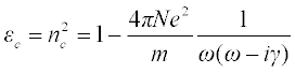
with:

for γ the loss (friction) coefficient and ωc the plasmon frequency, while such expressions can be generalized for multiple resonances (Roberts, 1955).
In real materials the electron mass should be replaced by the effective mass m* = ħ/∂2 E/∂k2 and the time constant τ = γ−1 is typically of the order of 10−15 to 10−13 s and describes the electron relaxation. Collisions with lattice imperfections, including phonons, impurities, vacancies and dislocations, are directly related to this prime cause of absorption and loss. At relatively low frequencies, below the plasma frequency and the relaxation rate (ω << τ−1) the metallic behaviour is evident with α ~ (2πσ/ω)1/2 and penetration depth α−1 diminishes at very high conductivities yielding unity reflectivity, as described by the Hagens-Rubens relation R ~ 1 – 2 (2πω/σ)1/2. However, for the optical frequencies above the plasmon frequency and the relaxation eigenfrequency ω >> τ−1. extinction decreases, k << 1, manifesting a dielectric behaviour for the metallic material. In this regime, however, interband transitions and direct photo-ionization become profound and are the principal causes of absorption in the material. Electrons may be excited to the continuum and transfer their energy to the lattice non-radiatively, resulting in temperature increase. In fact, at room temperature free electrons may have velocities of the order of 106 ms−1 (Fermi level). Under low radiation intensities, electrons are accelerated under the action of the e/m field of the incident radiation. This is a small perturbation of the random motion and electron collisions act to randomize and restore the distribution effectively with a time constant τD. For metals the Fermi level is much larger that kT and in practice the available states are only found close to the Fermi level. Therefore, electrons gaining energy from the optical field tend to occupy these states and thus determine the value of relaxation, τ, for the total distribution. The relaxation time constant, τD, in this case refers to the previously defined rapid processes in the time scale of τ ~ 10−13–10−15 s. This random redistribution of electrons having energy larger than kT contributes to the heat content of the material. There is, however, a significant difference between the randomization of electron momentum and the randomization of energy gained through interaction with the optical field, which is certainly slower, and it is represented by the energy relaxation time constant, τE. Considering a scattering cross-section σ and a density of scattering centres, N, the mean free path is lfree = (σN)−1. This parameter determines the efficiency of energy transfer to the lattice, providing energy and momentum conservation.
The increase of light intensity implies the application of a high electric field of several Volts/cm which strongly accelerates the electrons. ‘Hot electrons’ are thus produced that are moving fast under the influence of the e/m wave. The cloud develops its own high electron temperature Te. This electron energy gained is exchanged with the lattice and leads to equilibrium described through this energy relaxation time constant, τE, which becomes an important parameter. With the exception of aggregates and interfaces in the solid, especially found in alloys and nanocomposites, impurity scattering is quite low at room temperature and phonons are the main scattering centres. The acoustic branches cannot be responsible for a large velocity change associated with energy transfer, since they are limited by the speed of sound in the solid. Therefore, the largest energy loss mechanism is through scattering by optical phonons where the loss per collision is of the order of kΘD, where ΘD is the Debye temperature. The inclusion of structural inhomogeneities results in dramatic energy loss. Overall such processes yield large increase of temperature eventually leading to thermal transformations, melting and evaporation, phenomena fundamental in materials processing. In the case of significant energy excess, beyond the levels of the unperturbed electron gas, the rapid increase of its energy content yields strong electron collisions capable of producing avalanche ionization and explosive ablation of the material with plasma formation.
The evolution of effects in various laser intensity regimes are considered and discussed in the following sections of this chapter.
1.4.2 Absorption and energy transfer in semiconductors and insulators
Semiconductors and insulators constitute another important category exhibiting individual behaviours. The absorption processes are presented schematically in Fig. 1.3 with the typical absorption curve describing the various processes.
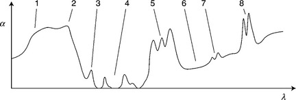
1.3 Absorption processes in a model semiconductor from the X-ray and extreme UV region (1) to beyond the FIR region. The fundamental absorption edge (2) embraces possible excitonic states (3) and is followed by impurity absorption states (4). The free electron IR absorption edge (6) with molecular coupling (5) and direct photon–phonon interactions (7), are followed by long-wavelength spin and cyclotron resonances (8), which are of minimal importance in our case.
The various regions and associated specific processes are as follows:
(i) In the UV spectral range (1–2) strong absorption is caused by interband transitions from the valence to conduction bands. The fundamental absorption edge, 2, may be in the visible or near-IR for semiconductors. The absorption coefficient is typically above α ~ 105 cm−1. For larger photon energy in the X-ray region and beyond, this absorption decreases rapidly. The energy and momentum conservation, respectively, ΔE = Ef – Ei = ħω(β) and kf – ki = β are valid. Towards the longer wavelengths, the edge 2 defines the limit of the band gap, Eg = hv, and yields a sharp decrease of absorption. Usually at low temperatures for bulk materials, this region comprises excitonic states, 3. Rayleigh and Mie scattering are always present and result in increased coupling effects.
(ii) Further to the exciton states, 3, absorption is due to impurity centres in the gap, 4, which become ionized. Intraband absorption concerns also the case of free electrons in the conduction band or holes in the valence band. High intensities may yield reflectivity increase due to free electrons. In contrast to the metallic behaviour, this type of absorption depends on the electron density and is limited. Electron density in insulators is negligible. For photon energies below the energy gap, hv < Eg, absorption decreases with ω2, defining the free electron absorption edge, 6, that extends to the lowest limit of the energy gap. Impurity absorption changes considerably the behaviour of the materials and has dramatic effects in the overall response. In the band gap where the material can in practice be fully transparent, ion centres or other imperfections lead to strong resonance absorption which depending on the matrix environment can present a quite broadened response. A linear absorption spectrum is thus observed. Characteristic examples here are the hydroxyl (O-H) bonds in silica, of special interest in optical fibres, which limit the NIR transmission, and the C-H bonds in polymers, with several chromophores producing dramatic absorption in the otherwise transparent materials.
(iii) In the far-IR region (> 20 μm) the interactions between photons and phonons are direct, in region 5. Photons interact with the optical modes due to dipole moment of the lattice and the comparable energy content (0.05–0.02 eV). At high frequencies the probability for the participation of multiphoton processes increases and absorption constants can approach 105 cm−1 in polar crystals. In covalent crystals, however, smaller values of 10–100 cm−1 are observed. Lattice imperfections again play a crucial role and lead to nonlinear coupling. Very low frequency effects, 7–8, such as cyclotron and spin resonances are not important in our case.
(iv) High laser intensities reveal a range of nonlinear processes in solids, owing to non-harmonic driving of the materials polarization as P ~ χE + χ(2) E2 + χ(3) E3 + …. Further to the frequency generation processes, nonlinear Raman or Brilluin scattering induce strong radiation coupling to the solid via stimulated processes. Of great significance here is the nonlinear absorption process occurring at high laser intensities, in which the simultaneous presence of multiple photons results in excitation and ionization of atoms and molecules, even by use of low photon energies. The response is analogous to the nth-power of the intensity as, Φ ~ In, where n is the process order defined as the number of participating photons.
In the above context, high-intensity laser radiation can be coupled directly or indirectly to the molecular or lattice vibrational modes depending on wavelength and release its large energy content locally in the material bulk. The large temperatures induced can drive pyrolytic reactions which can have a dissociative or a synthetic character. Such processes may be realized not only in solids, but also in the liquid and gas phase, while the involved processes may assume a chemical, a physical or a mixed character. Laser beams are ideal for delivering their energy on the spot and pyrolytic processing takes advantages of this effect. In addition, the thermal properties of the sample under processing must have appropriate values. In particular, thermal diffusivity is crucial for localized high temperature processing. In addition, resonant absorption aids further, by allowing selective and efficient processing.
Photolytic processes are also of particular interest. In this case highly energetic photons are used to activate photo-dissociative reactions which decompose the material by breaking molecular bonds. These operations make use of single or multiple photons of the UV, visible and up to the near-IR region. They may be realized under subtle thermodynamic equilibrium or take an explosive, photo-ablative character, depending on the irradiating intensity and materials nature. This process, however, can result in materials deposition by use of precursors in reactions of the type MX + hv → M* + X, where * denotes the possible presence of an excited state. Classic examples are the cases of metal-organic dissociation employed in Laser-assisted Chemical Vapour Deposition (Laser-CVD) by use of alkyl, alkalide, carbonyl and hydride precursors.
In molecular solids, transitions are realized between vibrational levels of the molecule (Frank-Condon principle) and high photon energy may lead directly to repulsive states and bond breaking. Depending on light intensity and nature of the material, in particular the state of impurity content, imperfections, water/analyte level of organic materials, a variety of processes may take place. Synthetic chemical reactions among molecular species are a major processing class, with photosynthesis of organic compounds found widespread in nature. Photo-polymerization is also a principal delegate. Further to conventional UV light and electron beam methods, laser lithography is also a well-established micro-fabrication process and it is widely deployed in micro-electronics and micro-engineering industries, due to the reliable process integration of deep-UV KrF (248 nm) and ArF (193 nm) laser sources. Current trends discussed in this work relate to multiphoton laser lithography which enables stereo-lithographic processing with submicron accuracy, as addressed in the following chapters.
A number of further processes concern molecular photo-adsorption and photo-desorption by relatively low intensity laser radiation (Georgiou et al., 1998). Laser radiation may resonantly drive atomic ensembles and produce large perturbation of their thermal distribution and thus retardation and cooling (Letokhov and Minogin, 1979). In addition the use of enhanced optical near fields in the vicinity of nanostructures such as metal tips leads to selective surface patterning (Jersch and Dikmann, 1996). Such processes are of fundamental interest in surface science leading to selective deposition in the atomic and molecular level with prospective impact in several fields, especially in forthcoming deposition and patterning micro-fabrication applications.
1.5 Materials processing phenomena: appraisal of energy dependencies
Laser processing operations commence upon the absorption of radiation and follow the conversion of energy. Absorption is described by the absorption coefficient, α(ω), which is a strong function of materials nature and the frequency of light. The individual absorption processes and the transfer and conversion of the energy are characteristic of the specific materials class as analysed in the previous section. Nevertheless, the solid workpiece may differentiate its physical response to the incident radiation, depending on surface properties, structural defect and impurity content. All these factors can differentiate greatly the processes involved and the operations performed even by using the same substance.
To illustrate the dependencies on radiation power properties we refer to Fig. 1.4 presenting a schematic description of typical events evolving by increasing laser intensity. We include in our discussion both cases of CW and pulsed operation, in conjunction with appropriate energy transfer and diffusion issues, as follows:

1.4 Scale of processing: (a) Subtle, non-destructive processing by low intensity radiation with physical and chemical effects yielding thermal, synthetic and polymerization operations, (b) higher laser intensity may lead to two zone transformations, (c) increasing intensity produces evaporation of material and may lead to photo-ablation process (d) with directional plasma formation and ejection of particles in a non-Maxwellian distribution.
(i) At relatively low intensities < 104 W/cm2 the energy absorbed can heat rapidly the material, as shown in Fig. 1.4a. Depending on energy deposition rate by beam 1 and heat transfer properties of the sample 2, including heat conductivity and geometry, an elevated temperature profile is established. A high enough temperature is able to produce initially phase changes and transform the material of region 3. Provided appropriately short wavelength laser radiation may induce photochemical reactions in region 3, processes well known in photochemical synthesis and photo-polymerization. Region 3, the heat (or radiation) affected zone (HAZ) of the workpiece, may exhibit upgraded or degraded physical and/or chemical properties (hardening, polymerization, etc.).
(ii) Irradiating by a beam 1 of intensity above 105 W/cm2, the material, 2, may melt under thermodynamic equilibrium, as shown in Fig. 1.4b. The energy deposition rate must exceed loss by thermal diffusion and the overall energy transfer determines again the established temperature above the melting point. The melt region solidifies after removal of radiation. Heat affected zone 3 and re-solidification zone 4 are observed. This case is relevant to alloying, vitrification and the like processes.
(iii) The case of higher beam intensities of the order 106 W/cm2 is presented in Fig. 1.4c where melting and evaporation become profound. Vaporized material 5 is ejected in vacuum (or the ambient gas atmosphere) uniformly leaving considerable heat affected (3) and re-solidification (4) zones on the sample surface. As a result of this process a crater is drilled in the material and may be fully penetrating. In metals the prolonged interaction may lead to the formation of a highly energetic plasma-radiation coupled region in the crater, namely a dynamic keyhole effect. This highly energetic keyhole is responsible for deep-penetration materials processing (drilling, cutting, welding). In this intensity regime, the use of pulses of highly energetic photons, for example in the UV, can lead to molecular photo-dissociation and atomic desorption which may also undertake an ablative character.
(iv) With the use of well above 106W/cm2 intensities as shown in Fig. 1.4d, the energy of beam 1 is deposited very fast on the material. This regime is reached by use of short (nanosecond) and ultra-short (< 1 picosecond) laser pulses. The interaction with the material thus becomes violent and explosive with a highly energetic plasma plume, 5, produced, which has directional properties. This is the laser ablation regime evolving under unstable non-equilibrium thermodynamic conditions and in practice it is an explosive process. Material is ejected rapidly from the target and undertakes a thermal or a less thermal character depending on wavelength and materials nature. The ejected material is a mixture of plasma species together with molecular clusters and micro-particulates formed on ablation. This is a very complex process caused by several interdependent physical and chemical effects. Here the extent of regions 3 and 4 is smaller and a ‘cleaner’ cut is etched on the surface, with minimal thermal or radiation affected zones.
Depending on wavelength and pulse duration thermomechanical and chemical effects are induced and drive the process with respective modifications. Pulse energy and duration are both crucial as discussed in the next section. Laser intensity determines the absorption linearity and the energy deposition rate – both of importance in process quality. The fluence and total energy deposited on the workpiece are associated with the extent of the operation. They quantify the ablation zone and the process affected zones on the workpiece.
Laser materials processing is a multifaceted operation rich in science and technology. The complexity of the involved processes and the interdependency of effects make the analysis of the involved processes very difficult. Most topics addressed here are subjects of current research, especially as they relate to photonics and micro-engineering sectors. They are a challenging field with many open problems yet to solve, but many promises to be fulfilled.
1.6 Laser-based materials processing for photonics
Two main processing modes are met and have been applied in the growth and processing of photonic materials and devices. The non-ablative, nondestructive subtle operations concern mainly thermal and photochemical processes. Three-dimensional polymerization and more recent advances relating to further photophysical effects such as the application of radiation forces are fields open to research. The second major category concerns the application of laser ablation in the growth and processing of photonic materials and devices. This section provides a brief outline of the operations and highlights the unique features and the achievements of the original developments, discussed further in the following chapters of this book.
1.6.1 Subtle, non-destructive materials processing
Operations in this category cover a wide range of photophysical and photochemical effects and applications, making use of a wide range of available laser sources. We outline here the main topics in the field and point the reader to the following chapters for a detailed state-of-the art analysis.
Photophysical effects
While laser radiation is an important tool for metalworking and the microelectronics packaging industries, laser-based processing in photonics technology meets niche applications (Basting and Marowsky, 2005). Laser annealing has been widely applied for the phase transformation of semiconductor interfaces such as in thin film transistor (TFT) production, as well as for selective materials doping. Thus, laser offers selective processing in the material bulk (Gamaly et al., 2006) leading to structure modification, crystallization, optical poling glass and polymers, and the induction of nonlinear optical properties Along these lines, photorefractive processes represent a large class of refractive index modification of materials by the application of usually intense optical fields. The refractive index of a material can be tailored by structured light even at milli-Watt power levels. Such changes may relate to the excitation of specific impurity centres or vacancies resulting in localized refractive modifications. In several cases these effects are also associated with strong photochromism owing to the excitation of relatively deep levels which affect the absorption properties, especially by use of UV radiation. Characteristic examples concern silica and other glass bulk and optical fibres with significant impact for fibre grating technology and other widespread photonic applications.
Structural modifications can be induced even by low intensity laser beams in amorphous and glass oxides (Mailis et al., 1998), and also non-oxide chalcogenide glass materials (Gill et al., 1995). The strength and the permanency of these effects depend on materials, laser wavelength and radiation intensity in the interaction region. Dynamic processes may be based on relatively long-lived effects that relate to impurity state excitation. They are followed by electronic or ionic relaxation phenomena which provide a degree of reversibility to the original materials state after removal of the irradiation. Intense irradiation, especially highly energetic deep-UV photons, may yield permanent structural changes usually associated with structural deformations. These effects result in significant variation of the refractive index and provide the means for the fabrication of micro-optics, optical waveguides and other photonic devices. In this case the high-intensity electric field rather than thermal effects has effectively modified the internal structure locally in the bulk in the area of beam focus, inducing large optical nonlinearities. Such effects take advantage of multiphoton processes induced by ultra-short high-intensity pulses, while refractive filaments in silica bulk offer new possibilities for photonic structure fabrication in the future (Haglund, 2006).
Quite different processing operations are possible by the deployment of laser radiation forces (Sigel et al., 2002). The application of structured optical fields leads to the production of reversible structures. They are formed by compressive forces in semi-dilute entangled soft matter causing rapid osmotic extraction of the solvent and subsequent solidification, forming three-dimensional micro-objects, discussed in a later chapter.
Photochemical effects
Some of the most well-known photochemical processes are those met in the reduction of silver in photographic emulsions. The dissociation of silver halide produces silver nanoclusters which darken the emulsion and develop the image, via the reaction AgX + hν → Ag + X. This process can also be activated by a focused or an interfering laser beam and can produce optical gratings in the bulk or the surface, a toolbox for the advent of holography and its numerous applications. The reduction of metallic compounds by using light is today a source for nanocluster production and it is applied as an alternative to chemical reduction methods.
The exposure of photoresists in lithographic processes use routinely high power UV lasers in the industrial floor. The relatively narrow spectrum of excimer lasers emitting at 248 nm (KrF) and 193 nm (ArF) and the high-intensity radiation allow tuning of the resist properties. In addition pulsed exposure allows fast processing speeds and high industrial yield. Deep-UV exposure has been advantageous in reducing the feature size of lithographic processing to the 100 nm size for contact methods. Resist technology has thus been developed in recent years to cope with lithography towards the extreme UV range. A favourable candidate appeared with the development of high power F2 excimer laser emitting at 157 nm. Even though this radiation promised to provide reduction of feature size well below the state of the art, two main problems hindered the further deployment of the technology. First, the delivery of beams at 157 nm requires complex vacuum or nitrogen or noble gas purged transmission lines, which increases the complexity of the technology. Second, the highly energetic photon of 7.9 eV produces molecular dissociation of the photoresist and large amounts of debris which is deposited on masks or near field optics thus decreasing the efficiency and the accuracy of the lithographic process.
Current industrial developments in the micro-electronics and photonics industries incorporate high power UV laser lithography for large-scale production and multiphoton lithographic processing currently provides significant feature size reduction. This is caused by the use of the high-intensity section of the focused beam, which can be tuned to reach processing regions sized below the optical diffraction limits. In this context scanning laser lithography by femtosecond lasers leads to 3D structure development, as an evolution of conventional stereolithography. Complementary approaches relating to metallized structures have also been presented.
Further to the photo-polymerization processes, intense UV beams have been used for the deposition of metals and the growth of semiconductors, which can be realized in gas, liquid and solid environments. For example, the use of organometallic compounds has provided selective deposition of metals by photo-dissociative reactions such as M (–Cx Hy–) + hv → M↓ + CxHy↑. Metal hydrides have been similarly used with significant examples of amorphous silicon growth through silane decomposition in a series of photoreactions with deep-UV radiation to yield hydrogenated amorphous silicon through: SiH4 + hν → {SiH2 + 2H} + hν + Si → α-Si:H. Further applications involve oxidation and reduction processes with important examples being the production of reactive gas such as oxygen and nitrogen roots for oxide and nitride materials growth. The above processes may be realized as part of more complex processes such as physical vapour, molecular beam deposition, or laser ablative processes.
Photoreactions may also be used to achieve selective corrosive processing, while in most cases a suitable chemical equilibrium may be established depending on the application sought.
As a general rule the surface or bulk photochemical process embraces:
• Physical contact of the reactive species with the surface or dilution in the bulk
• Molecular adsorption on the surface of interest or establishment of a suitable composition which enables to develop further reactions
• Activation by laser radiation of suitable photon energy
• Production of reactive species and/or dissociation of products
The localization or not of the targeted process depends exactly on the laser interaction region and the extent and nature of the process achieved via localized or delocalized primary and/or secondary reactions. Effects may take an explosive character under intense illumination, thus denoting a rather ‘grey borderline’ between subtle and ablative processes.
In its relevant chapters this book provides an exhaustive account of state-of-the-art photophysical and photochemical processing, expanding in detail on the emerging research and future technologies.
1.6.2 Ablative materials growth and processing
Main ablation schemes
Of extreme fundamental and technological interest are the ablative processes realized upon interaction of solid or liquid materials with high-intensity laser pulses. Figure 1.5 depicts the typical interaction geometries implemented to date. In Fig. 1.5a, an intense laser pulse 1 is focused on surface of a solid target 2. The material absorbs the pulse energy and the material is explosively photo-ablated and forms a deposit, 3, on suitable oppositely positioned substrate, 4. In this case a pulsed laser deposition (PLD) scheme is realized, in which a highly energetic plasma plume 5 is formed. Figure 1.5b emphasizes the direct laser ablative processing scheme, where the target is etched with high precision by a highly focused beam or a complex pattern imaged on the surface, 2, at high resolution (Vainos et al., 1996). Both operations require laser intensity on target exceeding the characteristic threshold value. This threshold value is materials, surface and wavelength dependent. Below this value photo-desorption effects are possible which may be assisted by the substrate and/or the matrix.

1.5 Ablative processes: (a) backward ablation and materials deposition, (b) resulting surface etching, (c) forward ablation and micro-printing operation by laser-induced forward transfer and (d) selective film etching by forward materials ablation.
The forward ablation scheme (Bohandy et al., 1986) and the resulting micro-printing are illustrated in Fig. 1.5c. A transparent target substrate embodying a thin or thick film 5 is used. The irradiating pulsed beam is transmitted through the substrate 2 and is absorbed by the film 5 which is thus ablated at its interphase. The film material is expelled by the vaporized layer and forms a deposit 3 on the receiving substrate 4. The accuracy of this micro-printing operation performed by laser-induced forward transfer (LIFT) can reach the submicron levels (Zergioti et al., 1998). The remaining film is etched with high precision as shown in Fig. 1.5d, forming patterns, 3, of complementary design to those being micro-printed.
As we will discuss later in this chapter, both backward and forward ablation modes have achieved quite remarkable results. A wide range of materials, from glass and amorphous to high crystallinity epitaxial films have been achieved, while high precision direct etching has been proved a viable scheme capable for micro-fabrication.
Ablation mechanisms
Depending on the nature of the material, exposure of a local region of the materials interphase a (usually) focused high-intensity beam produces a rapid, abrupt vaporization of the surface material under thermodynamic non-equilibrium conditions. A superheated volume builds up close to the surface, the Knudsen layer, establishing internal temperature much higher than the vaporization temperature and a very high pressure. The density of this layer is proportional to the laser pulse intensity and the very small mean free path aids to equalize instantaneously the internal temperature of the layer.
This superheated layer is expanded from the near surface region expelling the possibly present ambient gas. Depending on pulse intensity this expansion may be subsonic (speed < Mach 1), sonic (speed = Mach 1) or supersonic (speed > Mach 1). In case of Mach 1, the external ambient pressure determines the vaporization. Mach 1 is a limiting case from which mass continuity is satisfied by the production of new vapour that adds on, finally creating a shock wave which propagates in the neighbouring materials.
This is exactly the case which onsets a series of laser interactions relating to the production of plasma as shown in Fig. 1.5. The intense light pulse produces fast ionization and the formation of a highly energetic directional plasma plume ejected as shown in Fig. 1.5a. Depending on the process parameters this plasma can be produced either by radiation heating of the ejected vapour, or by photo-ionization and direct photo-dissociation of the material or their combination. Plasma can be established under local thermodynamic equilibrium (LTE), governed by the Saha equation:
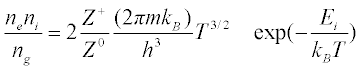
where respectively: ng, ne, ni are the number densities of atoms, electrons and ions, Z+ and Z0 the partial functions of ions and neutral atoms, me the electron mass, T temperature, kB and h are Boltzmann’s and Planck’s constants respectively, and Ei is the ionization energy.
Plasma extends and expands above the interaction region with a visible plume formed with temperatures reaching above 10000°K and pressures of the order of 104–107 Pa. Depending on intensity, particles are ejected at supersonic speeds, above 106 cm/s. Depending on the number density and radiation wavelength, plasma may absorb or reflect radiation, with such effects naturally becoming more profound by using IR radiation and long laser pulses.
Bearing in mind the above, it is important to underline that there is not an integrated theory available to date capable of describing well these complex phenomena. The thermal, photophysical, photomechanical and photochemical mechanisms are coupled together and constitute this explosive photo-ablation effect. The participating strength of each mechanism depends on the specific experimental parameters, which determine the evolution of events, and no absolute borders can be defined in all cases.
There are two types of ablation processes demonstrated to date. The backward ablation scheme described above (Fig. 1.5a) leads to a highly directional plasma plume which is characterized by multiple constituent components. The ejected matter comprises electrons and ionic species, neutral atoms, complexes, clusters and micro-particles, all ejected at different speeds from the ablation volume and following different spatiotemporal distributions. This latter effect is of extreme importance and offers significant advantages in applications requiring filtering of specific species. On the one hand the eroded material exhibits a minimal distillation effect, and the remaining part after ablation preserves the original composition of the target, and on the other hand, the ejected material also preserves its overall composition and can be deposited on a substrate achieving the original stoichiometry and in many cases the crystallinity of the target material. While there are exceptions, it has been observed that the less thermal the nature of the ablation process is, the more stoichiometric the expected deposits would be.
Influence of the actual experimental parameters
There are a number of important parameters which influence the ablation process, its nature and individual characteristics. These parameters are interdependent and affect not only the coupling of energy to the target but also the nature of the process itself as follows:
(a) Nature of target material, properties and surface characteristics.
(b) Wavelength of the laser beam and optical properties.
The nature of the target material determines the overall process and it is in full dependence on the laser parameters. The optical and physical properties are decisive in the development and evolution of these effects. Wavelength and surface properties are the main factors that determine the degree of energy coupling into the target, through the absorption property and the diffractive coupling effects induced by the surface texture.
According to our previous discussion, radiation incident on the planar surface is absorbed in the penetration depth, δ = α−1, where α is the absorption coefficient at the particular wavelength. The surface texture of spatial frequency comparable to the wavelength is acting to increase coupling of radiation, while sub-wavelength components are enhancing the most this nominal apparent absorption. The absorption of most materials in the deep-UV region is usually very high and the penetration depth is minimal, with the exception of highly transparent fluorides and related compounds. The penetration depth of UV radiation in metals is a few nanometres, except in some alkali. Infrared radiation can be more penetrating and thus energy is deposited in a larger interaction region than the UV.
The physical properties of the material undertake the next task of transferring this energy to the bulk. The nature of the material then determines the evolution of effects. In a case of solid having finite thermal conductivity, it is the combination of penetration depth δ and thermal diffusion length, Lth:
where, Dth is the thermal diffusion coefficient and τ is the laser pulse duration, which determines the interaction. In effect, the energy is deposited in a depth δ = α−1 and is converted to heat. During the laser pulse this heat is diffusing in depth Lth. A maximum energy accumulation effect is thus expected when during the irradiation time, τ, all energy deposited in δ cannot diffuse away, but remains in the interaction region with δ ~ Lth. Provided the pulse energy is high enough, this fact will lead to efficient ablation.
The intensity of the laser beam thus becomes the most crucial parameter. It relates to the energy deposition rate per unit area. While the pulse energy fluence is an important factor, it is effectively the pulse duration, τ, what governs the overall process. Figure 1.6 presents a range of effects evolving at different pulse length values and the respective intensities. In Fig. 1.6a CW radiation or a relatively long pulse 1, up to the nanosecond regime, irradiates the sample 2. Radiation may be absorbed within a specific volume, 3, by electrons in the valence band or impurity states, 4. This energy is transferred to the lattice via collisions and heats the material bulk. The more than few nanoseconds’ duration of interaction greatly exceeds the energy relaxation time (~ picosecond), meaning that interaction extends during the laser pulse irradiation. Region 3 is thermally transformed and melts under laser exposure. Non-destructive chemical effects may also take place.

1.6 (a) Long pulse effects from the cw to nanosecond pulse irradiation and (b) ultra-short pulse effects of sub-picosecond duration inducing multiphoton processing.
The use of high intensity, relatively long nanosecond laser pulses produces an electron avalanche inducing strong collisions with the lattice and finally causes materials breakdown by avalanche ionization yielding the photo-ablation effect. In molecular solids such as polymeric materials high energy photons may yield excitation to higher molecular states and enable the reach of dissociative states and molecular breakdown with minimal thermal effects. Even though in the case of polymer ablation thermal action cannot be excluded, the low thermal conductivity may yield a rapid passage to the evaporation state with minimal heat diffusion effects in the non-irradiated volume (Urech and Lippert, 2010).
In the nanosecond regime photo-ablation yields a visible ablated crater, 7, accompanied by a heat affected zone, 5, and re-solidification zone, 6.
Quite different effects are met by using high-intensity ultra-short pulses (Pronko et al., 1995). In Fig. 1.6b a sub-picosecond duration pulse, 8, irradiates the sample, 9. Irrespective of the laser wavelength a relatively high energy is confined in a small laser spot, thus leading to a smaller diameter interaction region, 10. This is caused by two effects: (a) the short interaction time becomes comparable to the energy relaxation time in the material and consequently it confines in space the whole event; (b) electrons are excited and become ionized by multiphoton absorption from the valence or impurity bands, or from a molecular state, as shown in 11 of Fig. 1.6b. The high-intensity pulse induces extreme acceleration and direct photo-ionization of electrons, leading to direct ablation. High laser intensities thus produce ablation with a smaller crater formation, 12, and minimal heat affected and re-solidification zones, 13. It is now proved experimentally that multiphoton effects enable high-resolution processing.
Laser ablation is characterized by intensity (and energy density) threshold effects and specific erosion (etching) rate behaviours. These are strong functions of the material, the wavelength of radiation and the pulse duration, through the processes outlined above. Multiphoton processing has a smaller ablation threshold and attains linearity of the etching rate. Radiation is absorbed and interacts in a shallow region near the surface, which yields high quality ablative processing. On the other hand, the energy density (fluence) value represents the total energy deposited per unit target volume and determines the extent of the overall etching process. In the long pulse regime, even in the nanosecond scale, the longer duration of interaction leads to larger ablation volumes, but with inferior etching quality effects. The ablation threshold is higher and the etching rate as a function of energy density shows a linear behaviour followed by a nonlinear saturation region. Figure 1.7 presents typical experimental data for threshold and etching (erosion) for polymer and metal substrates as a function of energy density. It is noted that the beam intensity is about 50 000 times higher in the ultra-fast case, though the energy deposited per unit area remains a quite important parameter. The material dependence is in any case distinguishable with the metal alloy showing clear improvement of the erosion rate and lowering of ablation threshold. It is worth noting here the difference between single and multi-pulse experiments. In the latter case the gradual deterioration of the structure results in lowering the apparent threshold and increasing the overall etching rates. Characteristic also is the difference between sub-picosecond and 20 ns pulses where the great difference in peak intensity leads to severe reduction of the etching threshold (Mailis et al., 1999).
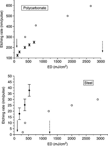
1.7 Typical experimental etching results for planar polycarbonate and polished steel substrates obtained by 20 ns (open circles) and 0.5 ps (closed circles) of KrF excimer laser beam at 248 nm, under identical focusing conditions. Solid arrows indicate single pulse etching threshold using 0.5 ps pulses and dotted arrows indicate the single pulse threshold using 20 ns pulses, both at 248 nm. (After Mailis et al., 1999.)
Considering the ablation process the intensity affects the plasma distribution leading a narrow cone of plume and matter ejection. Energy density also affects significantly the products of ablation. While femtosecond laser pulses were initially thought to yield highest quality ablation products and a smaller particulate content this has not been verified experimentally and nanosecond pulses are still seen to produce superior results in PLD experiments.
1.7 Specific laser processing schemes for photonics applications
Following our discussion of fundamental effects and processes we focus here on two specific laser processing schemes used in the fabrication of materials and devices, both relating to ablative processing. The reader is directed to the following chapters of this book for a presentation of schemes relating to lithographic and photorefractive processing.
Pulsed laser deposition is a prime application of congruent laser ablation having developed numerous devices and applications in the last decades (Eason, 2007). The method has been applied for the growth of photonic materials since the late 1980s, by exploring the nature of the process in the case of highly complex epitaxial oxide structures (Vainos et al., 1998), and proceeding to date with highly sensitive novel nanocomposites (Grivas et al., 1998). In all cases laser methods offer unique tools especially for materials that have proved hard to grow at high quality by conventional methods.
Micro-ablation effects are explored in micro-fabrication by etching and tailoring the surfaces and bulk of optical materials to produce photonic structures by use of nanosecond and femtosecond laser pulses. This latter scheme offers an alternative to well-established lithographic processing methods, with unique advantages in terms of single step, generic surface processing and in-the-bulk tailoring not available by other means. In addition, microprinting applications by laser-induced forward transfer (Fogarassy et al., 1992) are discussed here in the context of photonics.
1.7.1 Pulsed laser deposition (PLD) of photonic materials
Appraisal of methods and apparatus
The growth of photonic materials imposes stringent requirements on the nature of the ablation process, the materials used and the conditions applied. Photonics require extreme quality with respect to optical properties such as transparency, bulk homogeneity and surface quality, in addition to specific individual properties, such as composition, doping or other physical properties.
To comply with these requirements, extreme control of the process is required and a huge effort has been made in this respect. These initial efforts have been directed to ferroelectric and paraelectric oxides, such as respectively barium titanate (BaTiO3) and bismuth silicate (Bi12SiO20) as holographic photorefractive materials (Youden et al., 1991). This progress has been followed by further materials including garnets and sapphire, which led to the achievement of the first laser actions by PLD grown in Ti-Sapphire, Nd:YAG and Nd:GGG optical waveguides (Anderson et al., 1997a, 1997b). More recently, nanostructured thin film oxide materials for photonic sensor applications have been developed (Mazingue et al., 2005). The overall methodology is developed and presented in reference to the typical PLD experimental configuration presented in Fig. 1.8a.
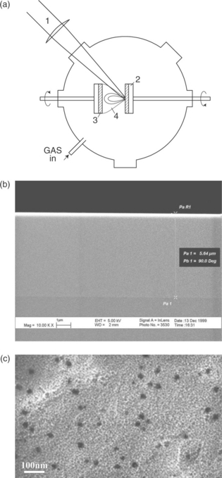
1.8 (a) Typical configuration of a PLD system. Includes a focused laser beam (1), target material (2), substrate with grown film (3), plasma formation and ablated material ejection (4). (b) Example of high quality laser glass composite grown for optical telecom applications and (c) indium oxide nanocomposite structure for light activation photorefractive effects.
A high or ultra-high vacuum (HV or UHV) reactor vessel is especially designed and constructed to incorporate optical windows and feed-through ports. The ambience of the vessel can be modified by gas injection and monitored by, for example, a quadrupole mass spectrometer (not shown). A pulsed laser beam 1 is directed through a transparent window and is focused on the target material 2. The target from which material is to be ablated may be in a solid crystalline, glass or sintered ceramic form. The target is usually attached on a rotating or translating holder platform, to ensure refreshing of the material undergoing ablation. This material is laser sputtered and grown as film, 3, on an oppositely placed substrate, which is usually a glass or crystalline plate, or wafer. A train of laser pulses, usually delivered at a repetition rate of a few Hz to some tens of Hz, ablate the target material producing a plasma plume, 4, which is directional and flushes the substrate. The ejected material is thus deposited on the substrate and grows a film, 3, on the substrate, while measures are taken to ensure uniform coverage in film growth. In Fig. 1.8b and 1.8c two distinct examples of photonic structures are shown: a highly compacted waveguide optical amplifier (Vainos et al., 1999) and indium oxide nanocomposite comprising nanocrystals and metal clusters in the amorphous matrix (Grivas et al., 2002).
While the overall laser sputtering process appears to be simple in its principle and provides a large flexibility in its operation, there are several interdependent parameters which need to be tuned for the successful growth of a specific structural composition. Even though there are various commercial systems available which operate reliably for specific relatively simple coating processes, the specific individuality and the interdependency of parameters make PLD a not yet industrially standardized process.
Interdependency of PLD processing parameters and methodologies
Several important issues determine the PLD methodology, with specific aspects of the scheme concerning:
(i) The nature of the target material: This determines the composition of the ablation plume and the stoichiometry of the deposit. The atomic and molecular composition and its constituents are determined by the density of the target and its form. There are several types of targets to be used: (a) solid crystalline target of material, (b) glass compound material, (c) sintered ceramic target and (d) liquid target used in specific cases. The more concrete and dense target produces better results in terms of particulate content and stoichiometry. In addition the rotation of the target is very important in refreshing the material and producing a relatively uniform composition over the duration of growth, the latter ranging from a few minutes to several hours. It is noted here that upon irradiation the target is usually severely eroded by ablation. Two effects are observed: (i) the composition of the target material is altered and in effect this differentiates the products of ablation over time and consequently the composition of the grown film; (ii) the morphology of the target is changed and this affects the direction of the plasma plume and the overall ejection of species, which consequently affects the growth process and the final composition and morphology of the grown film.
(ii) Laser parameters and ablation products: These are fundamental in plasma production and deposition and determine the nature of ablation. Following the previous discussion on ablation and plasma formation they determine the ablation process as follows:
(a) The laser wavelength determines the initialization regime and the type of ablation. Longer wavelengths produce thermal ablation effects, while the use of deep-UV laser pulses, such as those delivered by excimer lasers, is seen to produce advantageous results in terms of preserving the target stoichiometry in the ablated plume and reducing heat effects (congruent ablation). This preservation of stoichiometry is crucial in producing the desired composition on the film grown. Furthermore, high photon energy values are usually associated with a decrease of threshold intensity, with penetration depth also decreasing.
(b) The laser beam profile and the pulse intensity are crucial and determine the nature of the process and the energy of the ejected material. They affect the ablation threshold and the specific plasma plume formation and the ablation products distribution. The latter parameters are significant for establishing an efficient PLD configuration, in terms of substrate-target distance and geometry, the use of atomic, ionic, cluster or particulate ejects is crucial in the overall growth quality. The intensity of laser pulses determines the energy of the ejected products and the composition of electrons, ions, atoms, molecules, clusters and particulates, which subsequently travel in free space, vacuum or gas ambient and are incident on the target to grow the film.
(c) The total energy density on target determines the quantity of the ablated material and the overall deposition rate, by controlling the mass ejected per incident pulse and consequently the incremental thickness growth.
(iii) Experimental geometry and ambient atmosphere: The target-substrate configuration in particular is crucial in the growth of the thin film. The composition of the ablation plume is not uniform over the angular range. In addition the velocity profile of the ejected particles also varies in angle and depends on the nature of the particulates. The angular and velocity profiles are strong functions of the intensity profile on target and the specific geometry on the irradiated spot. Furthermore, the ambient atmosphere affects significantly the velocity profile and also the deposition through reactions of the ejected products upon collisions with the gas molecules. In effect, the presence of oxidizing and reducing gases affects greatly the growth process and can yield completely different compositions. Oxides and composites have been grown with variable stoichiometry (Vainos et al., 2004), as well as nitride materials, starting from metallic targets. These parameters are tuned in relation to the laser and other specifics of the scheme, in order to achieve the final growth goals.
(iv) Substrate temperature and physical properties: The growth of most inorganic materials and structures, especially in the form of crystalline epitaxial films necessitate deposition on substrates that are heated at high temperatures. The temperatures are characteristic of the specific material to be grown and for most oxides are above 600°C and exceed 1100°C for refractory oxides such as sapphire (Al2O3). More stringent requirements apply in the growth of epitaxial materials, in which case the choice of a suitably lattice matched substrate is necessary, in addition to the elevation at high temperatures. In all growth cases the highly energetic plasma plume is highly beneficial because the kinetic energy of the ablation products is transferred on to the substrate and assists to establish the proper thermodynamic conditions for growth. The net effect is that even by depositing at room temperature the produced films are quite compacted and exhibit higher adherence to the substrate, thus differing in strength and properties to those of similar composition grown by other sputtering methods. Several heating configurations have been employed in the growth of photonic materials commencing from conventional heating wires and filaments and progressing to ceramic elements. In these cases the contact of the heating plate with the substrate has been found to produce non-uniform temperature profiles which affect severely materials growth, in terms of uniformity, composition and crystallinity. Carbon dioxide laser heating methods have been developed in the last decades making use of beam-folding-mirror and light-pipe homogenizers as well as raster scanning methods coupled to temperature profile monitors by thermal imaging, all targeted to producing uniform temperature profiles in the substrate (Barrington and Eason, 2000).
(v) Process optimization – Film quality: While significant progress in the growth of materials has been made, the strong interdependency of parameters necessitates detailed optimization to be applied for each material or at least materials class. Furthermore, the spatially narrow and non-uniform distribution of ablation products creates difficulties and inhibits deposition on large size substrates with good uniformity. Typical deposition areas of the order of 1–2 cm2 are most usual. Special approaches using eccentric or planetary motion of substrate and target are explored to extend to larger substrates of the order of 5 cm diameter for generic growth. It should be underlined here that thermal laser ablation, for example by IR lasers, of single element materials, such as carbon or silicon or metal, may indeed provide appreciable results over relatively large areas of 5–10 cm diameter wafers, owing to reduced directionality and simple elemental composition. Nevertheless, this is not generally applicable, especially when using high-intensity UV pulses forming multi-component plasma to enable multi-element and complex compound growth. One very important issue in PLD growth is the presence of cluster and particulates in the ablated material, which is directed and incident on the substrate becoming integrated in the deposited film. Two effects are worth mentioning here: (a) the cluster and submicron particulates which become embedded in the film may act in various ways. First, they act beneficially assuming the role of growth centres assisting the creation of crystallinity. Second, they may act disadvantageously since they create scattering inhomogeneities especially by incorporating particles sized in the tens of nanometres range and larger. However, in other applications the incorporation of such particulates has also been seen to act advantageously in creating nanocomposite materials, in which an amorphous and finely structured matrix hosts crystalline nanoparticles which have been produced by the ablation process, (b) It is usual to observe relatively large particles on the surface of the film. Especially those sized several hundred nanometres to micrometres create significant problems in photonics applications producing considerable optical scattering and waveguide losses, the latter being deleterious in highly demanding laser applications. There have been several schemes proposed aiming to reduce particulates by use of gas streams, velocity filters in the form of mechanical shutters, electromagnetic filters to steer the plasma and others. However, in view of the above discussed central use of nanoparticulates in crystalline growth and the formation of nanocomposites it is the specific application and the target operation what will dictate the appropriate methodology.
(vi) Advanced multi-target operations: The development of PLD systems is to date in a quite advanced state, although full automation to the degree of industrial standardization of the scheme has not yet been achieved. Systems available to date offer significant flexibility and considerable ability for generic operations by use of multi-target systems which allow multi-compound growth, multi-layers and complex dopants, in amorphous and crystalline growth results. Those use advanced environmental control and target and substrate motion protocols for growth control. Relevant issues and current advances are presented in the following chapters.
In conclusion, PLD has proved to be a quite versatile growth tool which can be adapted to the application needs. While the system is quite flexible, the very nature of the process has not yet allowed industrial standardization and reliability for large-scale production. The limited area and uniformity of deposition, together with the difficult control of parameters in large-scale and long-run operations are some present impediments. The latter yields an overall incompatibility with the existing micro-electronics and photonics foundry, thus limiting wide exploitation of the scheme.
Advanced schemes for photonics are discussed in a later chapter.
1.7.2 Micro-ablative processing operations
Laser micro-etching operations
The use of laser beams finely focused in the micron scale produces materials micro-ablation. This operation is limited in the micron or submicron size laser spot area and requires relatively low pulse energy in the range of a few milli-joules. In this regime the strong focusing in micron size spots of nanosecond pulses leads to extremely high intensities in the GW/cm2 range corresponding to energy density values of several J/cm2. These values are well above the ablation threshold of most materials including the highly transparent glass and crystalline compounds. The micro-ablation process thus leads to a series of processing operations allowing direct materials treatment spatially. These are now considered viable as alternatives to well-established lithographic methods, offering specific advantages and unique features as analysed here (Mailis et al., 1999).
Figure 1.9 provides an outline of a direct laser micro-fabrication station. The beam, 1, is delivered by a laser source (not shown) and is transmitted through a beam-shaping optics system, 2. The system performs beam expansion, filtering and possibly homogenization. The processed laser beam is directed through a folding mirror, 5, into a focusing objective, 3, which delivers the radiation onto the workpiece, 4, for processing. This workpiece is positioned on a platform allowing controlled x-y-z motion to enable focusing in the z-direction and x-y surface processing. It is noted here that depending on the specific configuration folding mirror 5 may be replaced by a raster scanning system, especially to be used with long focal length focusing. The overall processing area is monitored by ocular system, 6, which may include video imaging. We note here that such a system may be used in projection lithography in which case the laser intensity and power throughput needs may be reduced in favour of resolution.

1.9 Schematic of a direct laser micro-fabrication station. Includes laser beam (1), beam-shaping optics (2), focusing optics (3), workpiece for processing (4), folding system (5) ocular observation and monitoring system (6).
The operation of the system is assisted by the controlled motion of the platform especially by use of high precision nanomotion-motorized stages controlled by position encoders currently available with sub-100 nm accuracy. This allows precise processing of the workpiece in raster scanning and/or vector scanning modes. In addition, the beam-shaping system may comprise a suitable imaging mask or diaphragm which is projected onto the surface of the workpiece for direct etching of complex patterns such as holographic patterns and images, in conjunction with beam homogenizers.
The above imaging operation mode is considered to be most appropriate as it allows precise intensity control to be applied in the system through calibration procedures. It allows high precision ablative processing via high-resolution imaging, yielding controlled intensity profile and pattern transfer onto the workpiece. This scheme, combined with absolute motion control, enables high precision direct processing. It is worth underlining that the use of a focused beam is not always appropriate due to the Gaussian or other highly peaked beam profile at the waist which may lead to inhomogeneous processing. Nevertheless, in some cases this allows a type of super-resolved processing in the sub-wavelength regime (previously shown in Fig. 1.6b), utilizing only the high-intensity part of the beam, while the beam shoulders have intensity below the required ablation threshold.
Figure 1.10 depicts the first developed examples of micro-fabrication of computer-generated holographic optics etched directly on the surface of acrylic and polished stainless steel plate with their optical reconstructions having appreciable finesse though non-optimal configurations have been applied. Fig. 1.10c shows a Fresnel micro-lens of about 500 μm diameter. Fig. 1.10d shows a polymer optical fibre processed for sensor applications with long light coupling slot. This unique operation proves the generic processing capability of the scheme. Such operations benefit from the nature of ablation which is able to cope with different materials of composite nature without concern for differential erosion or preferential etching effects, provided the intensity is well above the ablation threshold. The quality and the speed of processing depend clearly on the laser parameters and the physical properties of the material. All issues discussed previously concerning the surface quality and the ablation mode established for processing also apply here. Bearing in mind the sensitive and the precise nature of the operation, the laser parameters must be tuned exactly in relation to the physical properties of the workpiece and the application sought in order to achieve high quality results. It is clear that excessive intensity may cause severe damage to the sample, while reduced intensity may lead to gradual deterioration of surface quality, making the required process impossible.
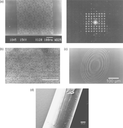
1.10 Direct micro-fabrication by UV laser radiation: Computer-generated holograms etched by direct ablation on (a) acrylic using 0.5 ps excimer laser pulses at 248 nm and optical reconstruction of interconnect matrix (b), stainless steel plate etched with computer-generated hologram using 20 nanosecond excimer laser pulses at 248 nm, (c) Fresnel lens element etched on polymer deposited on fused silica and (d) processed polymer optical fibre for sensor applications (unpublished). (After Vainos et al., 1996, Mailis et al., 1999 and unpublished data.)
Specific examples of photonics-related processing include the production of surface relief patterns, the production of micro-lens arrays, the processing of optical fibres and the tailoring of waveguide structures, as well as photonics packaging applications. The main advantages of the direct laser processing operation are drawn from its materials generic nature and the flexibility of application on surfaces of arbitrary geometry, practically on every solid surface. The scheme has been recently explored successfully in the fabrication of authenticity micro-holograms for security applications in the frame of the EU project initiative ‘HOLAUTHENTIC’, which resulted in a laser-based authentication system.
Laser micro-printing approaches
A complementary operation has been developed for photonics applications by use of the typical micro-fabrication station (Fig. 1.9). The material to be transferred is deposited on a transparent ‘carrier’ substrate as previously presented in Fig. 1.5c. An ultra-short laser pulse irradiates the film after transmission in the carrier plate and ablates the material at the substrate–film interphase. The net result is the ejection of the material in free space, propelled by the ablation gas products, and its deposition in the nearby positioned substrate. Figure 1.11 presents the dynamics of this forward ablation process by Schlieren imaging of the ejected material in free space (Zergioti et al., 2002). The velocity of the ejected material is a function of intensity of the laser pulse and determines the kinetic energy which is in turn deposited on the substrate. It is worth noting here that this operation can be performed either in vacuum or in gas atmosphere, while velocities in the range of 1 Mach have been recorded. It is noted that in this particular case the produced ablates are expanding in flight, while in other configurations the solid or liquid ejects are propelled and deposited on the substrate. This is the case with either metal targets or inorganic deposition by use of dynamic release layers, which rapidly photo-dissociate and detonate upon absorption of laser radiation.
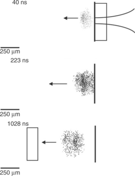
1.11 Dynamics of forward micro-ablation process. (After Zergioti et al., 2002.)
Figure 1.12 presents the first laser micro-printing operation in the submicron regime by using a single 0.5 ps laser pulse at 248 nm. Series of 700 nm diameter metallic Cr dots deposited on glass, silica and silicon substrates show excellent adherence, a fact which verifies the energetic nature of the process. By using a modified deposition cell micro-printing on optical fibres has been possible, as shown in the examples in Fig. 1.12b for dot series on D-fibre and high curvature etched cylindrical fibre. Such operations may lead the way to photonic sensor applications, enabling enhanced optical coupling and advanced interrogation.
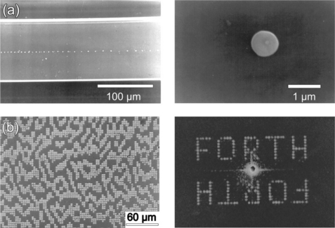
1.12 Micro-printing of (a) submicron chromium dots on the planar surface of D-optical fibre and (b) computer-generated hologram with its optical reconstruction by a HeNe laser. (After Mailis et al., 1999 and Zergioti et al., 1998.)
While the first application of laser-induced forward transfer concerned the repair of photomasks, the reduction of printed patterns and the high quality of deposits led the original developments in the field of photonics. Micro-printing operations thus first addressed the fabrication of photonic micro-structures in the form of computer-generated holograms of metals and metal-oxides.
Since these original developments several techniques have been developed for photonics applications, with most recent advances relating to the fabrication of waveguide devices by depositing metallic Ti stripes on lithium niobate for subsequent in-diffusion for waveguide fabrication. Further developments involve the use of polymeric dynamic release layers (Banks et al., 2008), which upon photo-dissociation produce a considerable amount of gas that enables efficient propulsion of the transfer layer, used especially in cases of transferring inorganic oxides, such as GGG and YAG laser garnets. It is worth mentioning that the method has so far allowed the deposition of submicron metal nanodroplets, achieved currently in the range of 500 nm and below to 300 nm diameter, by using amplified femtosecond Ti-Sapphire laser pulses in forward and backward transfer modes. Metallic films show a most suitable behaviour for decreased feature size, because the film melts locally releasing nanodroplets due to the unstable hydrodynamic conditions induced that enable propelling of matter to the oppositely placed substrates.
A case of global laser-based micro-fabrication
In Fig. 1.13 an example of a global laser-based device fabrication approach is presented (Koundourakis et al., 2001). The process commences with the PLD of metal oxide. In this specific case a non-stoichiometric mesoscopic indium oxide (InOx) nanocomposite is grown by reactive PLD using metallic indium target as shown in Fig. 1.13a. The material is deposited by use of nanosecond laser pulses at 248 nm on fused silica substrate. Its structure comprises several defects in the form of oxygen vacancies and metal nanoclusters, which enable charge transfer processes to evolve leading to variations of its electrical and optical properties. The latter effects lead to holographic recording in the material due to localized photorefractive effects induced by interfering UV laser beams.

1.13 Exclusively laser-based fabrication process producing active diffractive indium oxide diffractive elements. (a) PLD of the InOx parent film on carrier plate, (b) micro-printing of InOx grating, (c) functionality testing by diffraction experiments under the activation of a UV beam, (d) AFM image of a part of the InOx grating, (e) response of diffraction efficiency enhancement upon UV illumination. (After Koundourakis et al., 2001.)
This thin-film-on-carrier-plate structure is used in the laser processing station to micro-print a diffraction grating on a transparent glass plate by 0.5 ps 248 nm pulses, as presented in Fig. 1.13b. This grating is fabricated by repetitive transfer of grating lines sized in the micron range. We note that the build-up of the grating is achieved by precise relative positioning of the carrier plate and the receiver substrate, with the distance between film carrier and substrate kept in the few microns range.
The functionality of the deposited structure has been investigated by diffraction experiments under UV illumination at different temperatures. Fig. 1.13c depicts the typical experimental configuration used for functionality testing. The inset Fig. 1.13d shows an atomic force microscope image of the final diffractive structure. A UV laser beam is turned on and off and the diffraction efficiency of the micro-printed grating is altered within a certain response time determined by the participating charge transfer processes. In a manner identical to the parent InOx nanocomposite material, the refractive index of the grating is altered by the illuminating UV beam. This produces changes in the observed diffraction efficiency as shown in Fig. 1.13e in a similar time scale to that observed in the original ‘parent’ material.
It is worth mentioning that the alternative approach would be the lithographic processing of the planar film in order to produce the desired diffraction grating with expected similar results. Further to the complexity of this multi-step processing operation, a unique advantage of the laser-based scheme is drawn from its potential to produce micro-printed structures of arbitrary design on practically every given surface of arbitrary morphology, even of high curvature or discontinuous geometry, with no restriction. This is the significant advantage of the scheme in addition to the generic and inert processing nature of laser ablation. Indeed, as discussed above, lithographic approaches involve steps of wet deposition of masks, possibly followed by chemical or reactive etching which affects the nature of sensitive materials.
1.8 A suite of emerging concepts driving future trends
Direct laser processing schemes have emerged as viable alternatives to well-established fabrication and processing methods. Among the several open fields, we may focus on two regimes and distinguish them with respect to the intensity of participating processes corresponding to subtle and explosive operations.
Further to the widespread conventional laser lithography and laser surface annealing applications, relatively low power radiation induces photophysical and/or photochemical effects which directly modify the nature of the materials and yield photonic structures of extreme importance, such as waveguide networks, diffractive elements and switches or three-dimensional photonic structures for advanced coupling, filtering and sensing operations.
The second category embraces high-intensity operations associated with ablative materials photo-dissociation or explosive reactions leading to materials synthesis. Significant advances in this category concern the growth of photonic materials by PLD methods, in effect verifying the suitability of the method for the production of high optical quality and low loss materials suitable for photonic devices such as laser sources, waveguide circuits, switches and holographic storage.
Laser-based materials growth and processing exhibits unique advantages which concern the direct and non-contact nature of the operation. The required effects are induced usually by single-step operations and evolve simultaneously with laser irradiation. This offers high speed and flexibility in processing. In addition, the nature of the effects is quite generic, and, in effect, tuning of a set of parameters can suit to several materials and processing operations, with no further assumptions. The highly energetic photons of UV radiation, for example, induce photorefractivity, permanent or dynamic, in a variety of materials and has already led to Bragg grating and switching devices, as well as direct written optical circuits, tailored photonic crystal fibres and others.
Along the above lines, micro-ablative processing offers novel tools for direct etching and printing of materials in a single processing step, with no assumptions on materials nature or further compromises on the morphology and nature of the substrate or workpiece under processing. By these means, the etching of thin optical fibres or the printing of structures on a high curvature cylinder surface becomes possible, as does the internal processing of structures such as photonic crystals or multi-layer composites. In addition, large-scale ablation yields the production of multi-component plasma which is appropriate for the growth of complex multi-element epitaxial crystals or multi-layer stacks and nanocomposites exhibiting performances not available by other means.
Emerging technologies are multi-sectoral with novel concepts covering an interlaced network of techniques, materials and applications. The PLD growth of complex materials and devices is expected to follow niche routes leading to advanced photonics functionalities. While these systems may not be readily industrially acceptable, trends point to the exploration of their novel fabrication potential for advanced multi-layer and nanocomposite structures primarily of inorganic dielectrics and polymer-based structures. Laser devices, waveguide structures and sensors are current targets. The nanostructuring of semiconductor devices by laser radiation adds a new potential and exhibits characteristics compatible and integration ready with semiconductor processing foundries. The growth and the manipulation of devices will be realized by well-controlled PLD and surface processing techniques developed for specific classes of compounds. To this effect, it is yet unclear whether the full flexibility and the generic character of PLD will be exploited in the near future and technical limitations and specific features will prevail. However, there is scope and it is feasible to achieve appreciable size of growth by applying well-controlled multi-target planetary deposition approaches in perfectly mastered ambience.
Direct laser processing in the submicron scale is true and leads the way to nanoscale operations. In prime position are found deep-UV lasers but an important role will also be played by the available ultra-short lasers emitting high-intensity pulses at variable repetition rates. Solid state laser systems are favoured due to their compact size, reduced maintenance needs and overall ease of deployment, even though their cost remains high. The trend to ultra-short pulses is aiming to enhance performance based on multiphoton effects. The simultaneous interaction of two or more photons with the material enables the excitation of high energy states by use of low energy photons emitted by NIR lasers such as, for example, Ti-sapphire, Er-doped fibre lasers (EDFL) and the like. Furthermore, the attainment of super-resolution is realized by utilizing only the high-intensity ‘peak’ section of the beam profile, the lateral size of which can be smaller than the wavelength of light used when strong focusing with large numerical aperture objectives is applied.
Index manipulation in bulk devices and fibres also has great potential due to its novel character, while drawing benefits from multiphoton processing. The routine fabrication of Bragg fibre gratings with broad applications is a contemporary example of this rich area. Unique operations produced exclusively by laser light such as photorefractive and other light-induced structure modification effects are expected to offer enhanced performances combined with new materials and devices. Optical poling and phase changes, as well as localized thermal manipulation in glass and polymers are leading to advanced diffractive devices for telecommunications and sensing. The exploitation of these methods in speciality fibres and photonic crystal fibre structures represents new routes to follow in the future.
On the horizon for industrial application, ultra-short laser pulses for multiphoton lithographic processing and structure manipulation are important. Nano-fabrication will benefit by the use of ultra-short pulses in rapid prototyping and the direct construction of specialized three-dimensional devices by multiphoton stereolithography techniques enabling processing in the sub-wavelength scale. In this context structured fields come to play a very important role for the realization of innovative architectures. Of special interest are optical interference fields produced by femtosecond laser beams potentially enabling processing in a small fraction of the wavelength. Equally important are related multiphoton technologies which enable metallization, localized activation and micro-moulding processing, presenting a complete suite of multiphoton micro/nano-fabrication methods.
The following chapters of this book expose the richness of ‘Laser Growth and Processing for Photonics’ in a set of thorough reviews. The flexible methodologies developed in this emerging field are based on numerous scientific and technical achievements of the contributing authors and are expected to impact in several fields. Even though it remains unclear whether these methods will gain full reception and integration in the current industrial fabrication facilities, they hold a great potential and a living promise for new science and innovation in the years to come.
1.9 Acknowledgements
The original developments described in this chapter have been the result of successful research initiatives implemented in the frame of EU and national funded projects. In particular, the development of PLD schemes for photonics has been supported by the HCM EU-HCM ERB 4050 PL 92 1612: ‘Advanced Optical Waveguide Components and Systems’ and the INCO-Copernicus: ‘Inter-European PLD Network’. Diffracted optics and sensing systems have been developed through the support of EU-ESPRIT 6863: ‘Parallel Optical Processors and Memories’, the EU-GROWTH ‘Holographic Authenticity sensors (HOLAUTHENTIC)’, the EU-IST 2001 ‘Nanostructured photonic sensors (NANOPHOS)’ and various national PENED and ENTER projects funded by the Hellenic General Secretariat for Research and Technology, as well as the current HERACLITUS initiatives. The support of the ESF-COST Actions P2, P8, and MP0604 on advanced photonic materials is gratefully acknowledged. Many thanks go to Miltiadis Vasileiadis, Loukas Athanasekos and Dimitris Alexandopoulos for useful discussions and help with this chapter. The author remains grateful to all his collaborators who participated in the above research efforts – without their eminent contributions and hard work these developments could not have been realized.
1.10 References
Anderson, A.A., Bonner, C.L., Shepherd, D.P., Eason, R.W., Grivas, C.H., Gill, D.S., Vainos, N.A. Low loss (0.5 dB/cm) Nd: Gd3Ga5O12 waveguide layers grown by pulsed laser deposition. Optics Communications. 1997; 144:183–186.
Anderson, A.A., Eason, R.W., Hickey, L.M.B., Jelinek, M., Grivas, C.H., Gill, D.S., Vainos, N.A. Ti:Sapphire planar waveguide laser grown by pulsed laser deposition. Optics Letters. 1997; 22:1556–1558.
Banks, D.P., Kaur, K., Gazia, R., Fardel, R., Nagel, M., Lippert, T., Eason, R.W. Triazene photopolymer dynamic release layer-assisted femtosecond laser-induced forward transfer with an active carrier substrate. EPL(Europhysics Letters). 2008; 83 38003:1–6.
Barrington, S.J., Eason, R.W. Homogeneous substrate heating using a feedback controlled raster scanned c.w. CO2 laser with temperature monitoring. Review of Scientific Instruments. 2000; 71(11):4223–4225.
Basting, D., Marowsky, G.Excimer laser technology. Berlin: Springer-Verlag, 2005.
Bäuerle, D.Laser processing and chemistry. Berlin: Springer-Verlag, 2000.
Beesley, M.J.Lasers and their applications. London: Taylor and Francis, 1978.
Bohandy, J., Kim, B.F., Adrian, F.J. Metal deposition from a supported metal film using an excimer laser. Journal of Applied Physics. 1986; 60:1538–1539.
Born, M., Wolf, E.Principles of optics. London: Pergamon, 1989.
Chrisey D.B., Hubler G.K., eds. Pulsed laser deposition of thin films. New York: Wiley, 1994.
Cline, H.E., Anthony, T.R. Heat treating and melting with a scanning laser or electron beam. Journal of Applied Physics. 1977; 48:3895–3900.
Drude, P. Zur Elektronentheorie der Metalle. Annalen der Physik. 1900; 1:566–613.
Eason R.W., ed. Pulsed laser deposition of thin films: Applications-led growth of functional materials. Hoboken: Wiley, 2007.
Fogarassy, E., Fuchs, C., de Unamuno, S., Kerherve, F., Perriere, J. High Tc superconducting thin film deposition by laser induced forward transfer. Materials and Manufacturing Processes. 1992; 7:31–51.
Gamaly, E., Luther-Davies, B., Rode, A. Laser–matter interaction confined inside the bulk of a transparent solid. In: Misawa H., Juodkazis S., eds. 3D laser microfabrication: Principles and applications. Weinheim: Wiley; 2006:5–36.
Georgiou, S., Koubenakis, A., Lambrakis, J., Lassithiotaki, M. Formation and desorption dynamics of photoproducts in the ablation of van der Waals films of chlorobenzene at 248 nm. Journal of Chemical Physics. 1998; 109:8591–8601.
Gill, D.S., Eason, R.W., Zaldo, C., Rutt, H.N., Vainos, N.A. Characterization of Ga-La-S chalcogenide glass thin optical waveguides fabricated by pulsed laser deposition. Journal of Non-Crystalline Solids. 1995; 191:321–326.
Grivas, C.H., Gill, D.S., Mailis, S., Boutsikaris, L., Vainos, N.A. Indium oxide thin-film holographic recorders grown via excimer laser reactive sputtering. Applied Physics A: Materials Science & Processing. 1998; 66:201–204.
Grivas, Ch., Mailis, S., Eason, R.W., Tzamali, E., Vainos, N.A. Holographic recording mechanisms of gratings in indium oxide films using 325 nm helium-cad-mium irradiation. Applied Physics A: Materials Science & Processing. 2002; 74:457–465.
Haglund, R.F., Jr. Photophysics and photochemistry of ultrafast laser materials processing. In: Misawa H., Juodkazis S., eds. 3D laser microfabrication. Principles and applications. Weinheim: Wiley; 2006:139–175.
Ion, C.J.Laser processing of engineering materials: Principles, procedure and industrial application. Oxford: Elsevier Butterworth-Heinemann, 2005.
Jain, K.Excimer laser lithography. Bellingham: SPIE, 1990.
Jersch, J., Dikmann, K. Nanostructure fabrication using laser field enhancement in the near field scanning tunneling microscope tip. Applied Physics Letters. 1996; 68:868–870.
Koundourakis, G., Rockstuhl, C., Papazoglou, D., Klini, A., Zergioti, I., Vainos, N.A., Fotakis, C. Laser printing of active optical microstructures. Applied Physics Letters. 2001; 78:868–870.
Laude L.D., ed. Excimer lasers. Dordrecht: Kluwer Academic Publishers, 1994.
Letokhov, V.S., Minogin, V.G. Cooling, trapping, and storage of atoms by resonant laser fields. Journal of the Optical Society of America. 1979; 69:413–419.
Mailis, S., Anderson, A.A., Barrington, S.J., Brocklesby, W.S., Greef, R., Rutt, H.N., Eason, R.W., Vainos, N.A., Grivas, C.H. Photosensitivity of lead germanate glass waveguides grown by pulsed laser deposition. Optics Letters. 1998; 23:1751–1753.
Mailis, S., Zergioti, I., Koundourakis, G., Ikiades, A., Patentalaki, A., Papakonstantinou, P., Vainos, N.A., Fotakis, C. Etching and printing of diffractive optical microstructures by femtosecond excimer laser. Applied Optics. 1999; 38:2301–2308.
Mazingue, T., Escoubas, L., Spalluto, L., Flory, F., Socol, G., Ristoscu, C., Axente, E., Grigorescu, S., Mihailescu, I.N., Vainos, N.A. Nanostructured ZnO coatings grown by pulsed laser deposition for optical gas sensing of butane. Journal of Applied Physics. 2005; 98:74312–74316.
Pronko, P.P., Dutta, S.K., Du, D., Singh, R.K. Thermophysical effects in laser processing of materials with picosecond and femtosecond pulses. Journal of Applied Physics. 1995; 78:6233–6240.
Roberts, S. Interpretation of the optical properties of metal surfaces. Physical Review. 1955; 100:1667–1671.
Siegman, A.E.Lasers. Sausalito: University Science Books, 1986.
Sigel, R., Fytas, G., Vainos, N., Pispas, S., Hadjichristides, G. Pattern formation in homogeneous polymer solutions induced by a continuous wave visible laser. Science. 2002; 297:67–69.
Steen, W.M., Mazumder, J.Laser material processing. London: Springer, 2010.
Urech, L., Lippert, T. Photoablation of polymer materials. In: Allen N.S., ed. Photochemistry and photophysics of polymer materials. Hoboken: Wiley; 2010:541–568.
Vainos, N.A., Mailis, S., Pissadakis, S., Boutsikaris, L., Dainty, P., Parmitter, P.H., Hall, T.J. Excimer laser use for microetching computer-generated holographic structures. Applied Optics. 1996; 35:6304–6319.
Vainos, N.A., Grivas, C.H., Fotakis, C., Eason, R.W., Anderson, A.A., Gill, D.S., Shepherd, D.P., Jelinek, M., Lancock, J., Sonsky, J. Planar waveguides of Ti:Sapphire, Nd:GGG and Nd:YAG grown by pulsed laser deposition. Applied Surface Science. 1998; 129:514–519.
Vainos, N.A., Klini, A., Prassas, M., PLD grown waveguide amplifiers for telecoms. Private and Confidential Results for Corning Inc. 1999.
Vainos, N.A., Tsigara, A., Manasis, J., Giannoudakos, A., Mousdis, G., Vakakis, N., Kompitsas, M., Klini, A., Roubani-Kalantzopoulou, F. Metal/metal-oxide/metal etalon structures grown by pulsed laser deposition. Applied Physics A: Materials Science & Processing. 2004; 79:1395–1397.
Yariv, A.Quantum electronics. New York: Wiley, 1986.
Youden, K., Eason, R.W., Gower, M.C., Vainos, N.A. Epitaxial growth of Bi12GeO20 thin-film optical waveguides using excimer laser ablation. Applied Physics Letters. 1991; 59:1929–1931.
Zergioti, I., Mailis, S., Vainos, N.A., Papakonstantinou, P., Kalpouzos, C., Grigoropoulos, C.P., Fotakis, C. Microdeposition of metal and oxide structures using ultrashort laser pulses. Applied Physics A: Materials Science & Processing. 1998; 66:579–582.
Zergioti, I., Papazoglou, D.G., Karaiskou, A., Vainos, N.A., Fotakis, C. Laser microprinting of InOx active optical structures and time resolved imaging of the transfer process. Applied Surface Science. 2002; 197:868–872.