Chapter 4: Power Electronics and Electric Motor Drives of Hybrid Vehicle
The hybrid vehicle is a complex electrical and mechanical system. In all system configurations, a hybrid vehicle has two energy flow paths—electrical and mechanical. Mechanical energy flow is through a conventional powertrain, while the electrical powertrain provides a path for electric energy flow. In hybrid electric vehicle systems, the task of the electric motor and power electronics is to process and control electric energy flow to meet the vehicle demand power with maximum efficiency under various driving situations.
Power electronics generally combine electronic components, electric power, and control methodology. Their performance not only affects overall vehicle fuel economy and drivability but also makes up a major portion of the material cost of the vehicle. Depending on the type and configuration of a hybrid vehicle system, electric motor and power electronics can make up more than 25% of a hybrid vehicle material cost, which is almost equal to the expense of the energy storage system. Since DC electric energy conversion is implemented by power electronic circuits and the conversion efficiency is one of the most important performance considerations in hybrid vehicle system design, this chapter presents the basic principles of commonly used power electronics in hybrid vehicle applications.
4.1 Basic power electronic devices
Power electronic devices, or power semiconductor devices, deal with the control and conversion of electric power from one form to another. They play an intermediary role between the energy storage system and the propulsion motor in a hybrid vehicle. In order to achieve low cost-and high-efficiency power control and conversion in hybrid vehicle applications, power electronic devices always work in the switching mode. This section reviews the basic characteristics of commonly used power electronic devices in hybrid vehicles.
4.1.1 Diodes
A diode has one pn junction that makes it conduct one way only. The circuit symbol, structure, and i–v characteristics of a diode are shown in Fig. 4.1a–c. When the potential on the anode is greater than the potential on the cathode, the state of the diode is called forward biased, and the diode conducts. A conducting diode has 0.3–0.8 V forward voltage drop across the pn junction depending on the junction material, manufacturing process, and junction temperature. When the potential on the cathode is greater than the potential on the anode, the state of the diode is called reverse biased. In this state current flow is blocked and there is only negligible leakage current through the diode until the applied voltage reaches the reverse breakdown voltage (also called avalanche or zener voltage).
Figure 4.1 Symbol, structure, and i–v characteristic of diode.

Depending on the application requirements, a diode can be selected from the following types of power diodes:
All major diode parameters can be found in manufacturer's data sheets. Some of the principal ratings of diodes are as follows:
4.1.2 Thyristors
Thyristors are four-layer pnpn power semiconductor devices. These devices have three pn junctions and three terminals: anode, cathode, and gate. The electrical circuit symbol, pn junctions, and i–v characteristics of thyristors are shown in Fig. 4.2a–c. In contrast to power diodes, a thyristor has three operating modes: reverse-block mode, forward-blocking mode, and forward-conducting mode.
Figure 4.2 Symbol, structure, and i–v characteristic of thyristor.

When the potential on the anode is greater than the potential on the cathode, the junctions J1 and J3 are forward biased while the junction J2 is reverse biased, resulting in only a small leakage flow from the anode to the cathode. In this condition, the thyristor is in the forward-blocking, or the off state, and the leakage current is called as off state current. If the potential difference between the anode and cathode is increased to a certain value resulting in reverse-biased J2 junction breaks, the thyristor conducts as a diode and is in the forward-conducting, or the on state. Another way to change the state of the thyristor from forward blocking to on is to apply a positive gate current for a short period of time; furthermore, once the thyristor begins to conduct, the on state is latched and the gate current can be removed. It should be noted that the thyristor cannot be turned off by the gate, and it will continue to conduct like a diode until the forward current drops below the hold current IH or the thyristor is reverse biased. From the i–v characteristic curve, it can be seen that the gate current IG also controls the value of forward breakdown voltage. The bigger the gate current IG, the lower the forward breakdown voltage.
The principal thyristor ratings include:
4.1.3 Bipolar Junction Transistors
A bipolar transistor is a three-layer device with two pn junctions stacked opposite each other. If a transistor has two n regions and one p region, it is called an npn-type transistor; otherwise, it is called a pnp-type transistor. The three terminals of a transistor are the base, the collector, and the emitter. The electrical circuit symbols and structures of bipolar junction transistors (BJTs) are shown in Fig. 4.3a,b. The direction of the arrow on the emitter symbol distinguishes the npn-type transistor from the pnp type. The pnp-type transistor has an arrowhead pointing toward the base, while the npn-type has an arrowhead pointing away from the base. Based on the common emitter circuit with an npn transistor, the steady-state input and output characteristics are shown in Fig. 4.4.
Figure 4.3 Electrical circuit symbol and pn structure of transistor.

Figure 4.4 Steady-state input and output characteristics of npn transistor.

Operating Regions and Switching Characteristics As shown in Fig. 4.4c, a transistor has three operating regions: cutoff (off), saturation (on), and active. In power applications, a transistor works at cutoff and saturation regions as a switch. In the cutoff region, the collector–emitter voltage VCE is equal to VC as there is no current going through it, so the transistor acts as an opened switch in this state. In the saturation region, the base current is sufficiently high so that the collector–emitter voltage is very low; therefore the transistor acts as a closed switch in this state. In the active region, the transistor works like an amplifier to adjust the collector–emitter voltage based on the base current.
From the characteristics of a transistor, it can be seen that the base current needs to be high enough to allow the transistor to work as a switch. Thus, the on or off state of a transistor switch is determined by the base current, and the collector and the emitter are considered as two terminals of a switch. The values of VC and RC determine the operating points of a transistor from the DC load line shown in Fig. 4.4c.
In the on state, the collector–emitter voltage VCE should be near zero, so the collector current should equal (VC − VCE)/RC, where ![]() , is the saturation voltage at which the voltage drop across the collector–emitter terminals of a transistor is smallest. In other words, the collector–emitter voltage VCE is saturated when the base current is equal to or greater than the saturation current,
, is the saturation voltage at which the voltage drop across the collector–emitter terminals of a transistor is smallest. In other words, the collector–emitter voltage VCE is saturated when the base current is equal to or greater than the saturation current, ![]() ; at this point, the collector current is maximum and the transistor has the smallest voltage drop across the collector–emitter terminals. In the off state, the collector current IC should be near zero and the collector–emitter voltage VCE is equal to the supply voltage VC, which occurs when the base current IB = 0.
; at this point, the collector current is maximum and the transistor has the smallest voltage drop across the collector–emitter terminals. In the off state, the collector current IC should be near zero and the collector–emitter voltage VCE is equal to the supply voltage VC, which occurs when the base current IB = 0.
BJT Power Losses The BJT power losses mainly include the on-state power loss and turn-on/off switching loss. The on-state power loss is determined by the saturation voltage of the power transistor, and the lost power is given as ![]() . The switching frequency has a significant impact on the switching losses of a power transistor. For the power transistor, the higher the switching frequency, the more power loss in the transistor; however, the increase of switching frequency in a power device may result in a size reduction of other power components and power loss decrease in the components.
. The switching frequency has a significant impact on the switching losses of a power transistor. For the power transistor, the higher the switching frequency, the more power loss in the transistor; however, the increase of switching frequency in a power device may result in a size reduction of other power components and power loss decrease in the components.
4.1.4 Metal–Oxide–Semiconductor Field Effect Transistors
As mentioned above, the on or off state of a BJT is controlled by its base current; furthermore, a larger base current is needed to keep it in the on state. These characteristics make the base drive circuit design of BJTs very complicated and expensive. To overcome these drawbacks, a new type of power electronic device, metal–oxide semiconductor field effect transistor (MOSFET), was invented in the early 1970s. Compared to BJTs, MOSFETs are voltage-controlled devices and their switching speed is very high so they can be turned on and off in the order of nanoseconds. Power MOSFETs are the major power electronic devices in low-power, high-frequency converters. There are two types of MOSFETs: depleting and enhancement. The circuit diagram and i–v characteristics of an n-channel MOSFET are shown in Fig. 4.5a,b. The transfer characteristics of the n-channel depletion- and enhancement-type MOSFETs are shown in Fig. 4.6a,b.
Figure 4.5 Circuit symbol and output characteristics of n-channel MOSFET.

Figure 4.6 Transfer characteristics of n-channel depletion- and enhancement-type MOSFETs.

Steady-State Model Similar to power BJTs, a MOSFET also has three operating regions: on, off, and linear. As shown in Fig. 4.6b, an n-channel enhancement-type MOSFET will be in the off region if VGS ≤ VT, in the on region if VGS > VT and VDS > VGS − VT, and in the linear region if VGS > VT and VDS ≤ VGS − VT, where VT is the threshold voltage. The steady-state equivalent circuit of an n-channel MOSFET is shown in Fig. 4.7, where the transconductance gm and output resistance ro are defined as
4.1 ![]()
Figure 4.7 Steady-state equivalent circuit of n-channel MOSFETs.

Switching Model From MOSFET transfer characteristic curves, it can be seen that an n-channel depletion-type MOSFET remains in the on state even if the gate voltage VGS = 0 while an n-channel enhancement-type MOSFET remains in the off state at zero gate voltage. Therefore, n-channel enhancement-type MOSFETs are commonly used as switching devices in power electronic applications. The switching-mode equivalent circuit of an n-channel MOSFET is shown in Fig. 4.8, where Cgs and Cgd are the parasitic capacitances from gate to source and from gate to drain and Cds and rds are drain-to-source capacitance and resistance.
Figure 4.8 Switching-mode equivalent circuit of a n-channel MOSFET.

4.1.5 Insulated Gate Bipolar Transistors
To overcome the base-current control problem of power BJTs and improve the current-handling (power) capability of power MOSFETs, another power electronic device, the insulated gate bipolar transistor (IGBT), was developed which has the advantages of both BJTs and MOSFETs. The characteristics and specification of IGBTs allow them to be predominantly used as power electronics in hybrid electric vehicle applications.
Figure 4.9 shows the circuit symbol and equivalent IGBT circuit with three terminals labeled gate (G), collector (C), and emitter (E). An IGBT is a voltage-controlled device similar to a power MOSFET, and it is turned on by simply applying a positive gate voltage and turned off by removing the gate voltage. IGBTs have lower switching and conducting losses, share many attractive features of power MOSFETs, and require a very simple control circuit. Typical iC–vGE transfer and i–v (output) characteristics of an IGBT are shown in Fig. 4.10.
Figure 4.9 Circuit symbol and equivalent IGBT circuit.

Figure 4.10 Typical IGBT transfer and i–v characteristics.

IGBTs can be turned on and off in the order of microseconds, which is essentially faster than a BJT but inferior to MOSFETs. Current ratings of an IGBT module are as large as 1700 V and 1200 A.
4.2 DC/DC converter
In hybrid vehicle applications, DC–DC converters are commonly used to supply electric power to 12-V DC loads from the fluctuating high-voltage DC bus of an HEV/EV. They are also used in DC motor drives. To meet the fuel economy requirement of an HEV and electric mileage requirement of a PHEV/EV, the efficiency of an automotive DC–DC converter needs to be above 95%. This section presents the basics of DC–DC converters and commonly used DC–DC converters in hybrid vehicle systems.
4.2.1 Basic Principle of DC–DC Converter
The function of a DC–DC converter is to convert DC power from a voltage level (input) to other levels (outputs). In other words, a DC–DC converter is used to change and control the DC voltage magnitude; like an AC transformer, it can step down or step up a DC voltage source. The goal of current converter technology is that they be small and light weight as well as have substantial high efficiency.
The operating principle of DC–DC converters can be illustrated by Fig. 4.11a, b. To obtain the average voltage Vo on the load R in Fig. 4.11a, the switch needs to be controlled at the constant frequency (1/Ts) shown as Fig. 4.11b. Thus, the average output voltage Vo will be controlled by adjusting the on switch duration. The output average voltage Vo and the average load current Io can be calculated by the equations
4.2 ![]()
4.3 ![]()
Figure 4.11 A DC–DC converter.

The above control strategy is called pulse width modulation (PWM) control and is commonly used in DC–DC converters and DC–AC inverters. It is obvious that the longer the switch is on in a given signal period Ts, the higher is the average voltage of the device output. In PWM control, this characteristic can be described by the duty ratio D, defined as the ratio of the on duration to the switching time period Ts.
Sometimes, the term duty cycle is also used to describe the relationship of on-state time to the period of time of a given signal; furthermore, the duty cycle is expressed in percentage and a low duty cycle corresponds to a low voltage, for example, 100% duty cycle is fully on.
A PWM switch control diagram is given in Fig. 4.12, where the power electronics are switched on and off following the PWM control command at a constant frequency. In the diagram, the PID controller outputs the control voltage Vcontrol based on the difference between the desired output voltage and the actual output voltage of the DC–DC converter, and then the control voltage Vcontrol compares with the periodic saw tooth wave signal to generate the required PWM signal to switch the power electronics on or off, shown in Fig. 4.12b. The frequency of the periodic sawtooth wave establishes the frequency of PWM signal, while the duty ratio is generated based on the level of the control voltage Vcontrol. In practice, the actual switching frequency of a DC–DC converter can be from a few to a few hundred kilohertz depending on the detailed performance requirements and selected power electronic devices.
Figure 4.12 A PWM switch control diagram.

An important note on PWM switching control is that the PWM signal frequency has to be much higher than what would affect the load; otherwise it will result in discontinuous effect on the load. Depending on the load, a DC–DC converter may be operated in two distinct modes: continuous-current conduction and discontinuous-current conduction, so the switch control signal needs to be properly designed to have the converter work well in both operation modes.
4.2.2 Step-Down (Buck) Converter
The step-down converter, also called buck converter, produces an average output voltage that is lower than the DC input voltage. The circuit of a step-down converter, shown in Fig. 4.13, has a low-pass filter to avoid having the output voltage fluctuate between zero and the input voltage.
Figure 4.13 Step-down converter.

During the switch-on time ton, the circuit can be simplified asthe circuit shown in Fig. 4.14a with the relationships
4.5 
that is, the following dynamic equation can be established:

Similarly, during the switch-off time toff, the circuit can be simplified as shown in Fig. 4.14b with the relationships
4.7 
that is, there is the following dynamic system equation:

The dynamic characteristics of iL and vo can be obtained by solving the state space equations (4.6) and (4.8) at the given initial conditions.
Figure 4.14 switch on and off equivalent circuits of step-down converter.

4.2.2.1 Steady-State Operation
Continuou-Conduction Mode In the steady-state operation and when switch is on, the inductor voltage is equal to the input voltage subtracted by the output voltage: vL = Vin − vo. If we assume that the capacitor is very large and thus the ripple on the output voltage is very small, then the output voltage vo is approximately equal to the average output voltage Vo, that is, vL ≅ Vin − Vo.
Under this assumption, during the switch-on period of time, from equation (4.4), the inductor current can be calculated as
When the switch turns off, the inductor voltage changes direction and the current can be calculated as
From the inductor current flow, shown in Fig. 4.15, it can be seen that the current slope in the switch-on period is (Vin − Vo)/L and the current slope in the switch-off period is − V0/L.
Figure 4.15 Inductor current and voltage waveforms of buck converter.

During steady-state operation, the current waveform iL repeats from one period to the next, and the current at the beginning, IL(0), must be equal to the current at the end IL(Ts). Thus, from equations (4.9) and (4.10), we can obtain the following equation describing the inductor voltage waveform:
4.11 
that is,
4.12 
If we assume that the voltage waveform on the capacitor repeats from one period to another during steady-state operation, we can analyze the voltage on the capacitor as
4.13 
The foregoing equations imply the following in the steady-state operation:
Discontinuous-Conduction Mode In some cases, the amount of energy required by the load is larger than that stored in the inductor so the inductor is completely discharged. In these cases, the current through the inductor decreases to zero during the switch-off period, resulting the converter operating in the discontinuous-conduction mode. Figure 4.16 shows the switching state, inductor current, and voltage waveforms of a buck converter in the discontinuous-conduction mode of operation.
Figure 4.16 Discontinuous-conduction mode of operation of buck converter.

During the time tdisc in the discontinuous-conduction operation mode, the inductor current is zero and the power to the load is supplied by the filter capacitor alone. If the output voltage ripple is small enough, we have the following equations for the circuit shown in Fig. 4.13:

Since charge and discharge must be equal during steady-state operation, we have
4.15 
Solving for Vo yields
From the capacitor charge balance and equation (4.14), we have

From Fig. 4.16, the integration in the above equation is equal to
4.18 ![]()
Hence, equation (4.17) is rewritten as
Solve system equations (4.16) and (4.19) for Vo:

If the K is defined as above, the output voltage can be achieved when the converter operates in the discontinuous current mode as
4.21 ![]()
where D is the PWM duty ratio.
From the foregoing discussion:
4.2.2.2 Output Voltage Ripple
For switch-mode-based DC–DC converters, the output voltage rises when the switch turns on and falls when the switch turns off. This phenomenon is called voltage ripple and is mainly determined by output filter capacitance as well as affected by the switching frequency and filter inductance. The voltage ripple calculation is an important design calculation, but this section only presents very basic concepts. For more detailed information, the interested reader can refer to Mohan et al. (2003) and Erickson and MaKoimovic (2001).
From previous discussion, we know that the practical output voltage of a switch-mode DC–DC converter is a rippled DC rather than a solid DC and can be expressed as
4.22 ![]()
If we assume that the load resistor takes the average component in current flow iL(t) and the ripple component goes through the filter capacitor, the charge on the capacitor can be calculated based on the capacitor initial current iC(0) and final currents iC(ton), which are obtained from equation (4.14) and Fig. 4.16 as follows:
4.23 
4.24 
The stored charge in the capacitor shown in the shaded area in Fig. 4.17 is equal to the integration of the positive current flowing through it over time, that is,
4.25 ![]()
Thus, the magnitude of output voltage ripple on the load is equal to
4.26 ![]()
The voltage ripple on the high-voltage bus is an important parameter and needs to be less than a certain value in hybrid vehicle applications. The magnitude of output voltage ripple can be diminished by increasing the output capacitor, filter inductor, and switching frequency; however, the capacitor and inductor are normally selected based on cost and physical size, and a higher switching frequency generally lowers the converter's efficiency and may also raise the EMI in hybrid vehicle system applications.
Figure 4.17 Output voltage ripple of buck converter.

In the worst ripple case, we can assume the charge current Ib to up and down linearly as shown in Fig. 4.18b. di = ΔIb, dt = t1 = DT = 0.778 × 50 × 10−6 = 38.9 μs. Therefore, from equation (4.27) we have

Thus, the required inductor needs to be with 0.48 mH inductance.
Figure 4.18 DC converter with battery pack.

4.2.3 Step-Up (Boost) Converter
A boost converter is capable of providing the average output voltage at a level higher than the input or source voltage; therefore, the boost converter is often referred to as a step-up converter. The circuit of a boost converter is shown in Fig. 4.19, where the DC input voltage is in series with a large inductor acting as the current source. When the switch is on, the diode is reverse biased, and thus the output is isolated with input and output voltage maintained by the capacitor; meanwhile, the input supplies energy to the inductor. When the switch is off, the load and capacitor receive energy from the input and inductor so the average output voltage is higher than the input voltage. Corresponding with the switch state, the circuit can be split into two circuits, as shown in Fig. 4.20a,b.
Figure 4.19 Boost converter.

Figure 4.20 Boost converter with switch on and off.
In steady-state operation the waveform must repeat for each cycle, so the volt-second of the inductor must be balanced between the switch on state and the switch off state; that is, the integral of the inductor voltage over one time period must be equal to zero in the steady state. In other words, the shaded area A must be equal to the shaded area B in Fig. 4.21. If assume that the current through the inductor linearly changes, the voltage conversion ratio of a boost DC–DC converter can be obtained as
4.28 
The relationship between the voltage across the inductor L and the current flowing through it can be described by the following differential equation, and the current can be determined by integrating the voltage:
4.29 ![]()
When the switch is on, the inductor current can be determined as
4.30 ![]()
where Vin/L is the slope of the inductor current change when the switch is on. The inductor current when the switch is off is
4.31 ![]()
where (Vin − Vo)/L is the slope of the inductor current change when the switch is off.
Figure 4.21 Inductor voltage and current on continuous-conduction mode of boost converter.

Since the converter is in the steady state, the current waveform iL repeats from one period to the next; thus, the current at the beginning, iL(0), must be equal to the current at the end, iL(Ts). The input ripple current ΔiL, pp shown in Fig. 4.21 can be determined as
Similar to the analysis of the bulk converter, if we assume that the capacitor shown in Fig. 4.19 is big enough to absorb the ripple current passing through the inductor and the load resistor only absorbs the DC component, the output voltage ripple can be calculated based on the following charge balance equation on the capacitor. The detailed waveforms related to the output voltage ripple are shown in Fig. 4.22.
4.33 ![]()
The magnitude of the output voltage ripple is
Equation (4.32) shows that the ripple current reduces as inductance increases, while equation (4.34) shows that the ripple voltage reduces as capacitance increases.
Figure 4.22 Capacitor charge and output voltage ripple of boost converter.

From the foregoing discussion of the boost DC–DC converter we have:
4.2.4 Step-Down/Up (Buck–Boost) Converter
A step-down/up converter is also called a buck–boost
converter, and provides output voltage that can be either lower or higher than the input voltage. In addition, in a buck–boost converter the polarity of the output voltage is opposite to the input voltage. A schematic of a buck–boost converter circuit is shown in Fig. 4.23. The power switch can be a power bipolar transistor, MOSFET, IGBT, or any other device that is turned on (and off) by following a control scheme. The circuit is operated in two states, with the switch on and off. The circuits for these two states are shown in Fig. 4.24a,b.
Figure 4.23 Buck–boost converter.

Figure 4.24 Buck–boost converter with switch in on and off states.

When the power switch is in the on state, the input current flows through the inductor L and the input energy is stored in the inductor, and the output voltage is maintained by the capacitor C. When the switch is in the off state, the stored energy in inductor L will be transferred to the load R and capacitor C. The steady-state voltage and current waveforms of the buck–boost converter are shown in Fig. 4.25 in the continuous-conduction mode. These waveforms are obtained from the following derivation.
Figure 4.25 Inductor voltage and current in continuous-conduction mode of buck–boost converter.

As shown in Fig. 4.24a, in the steady state the inductor voltage equals the input voltage, which results in a linear increase of the inductor current iL(t) from the minimum value at the beginning, iL(0), to the maximum value at the end, iL(ton), of the switch on state as follows:
4.35 ![]()
During the toff state, ton < t ≤ Ts, the current falls linearly from the peak state iL(ton) to the initial value iL(0) = iL(Ts):

Therefore, the peak-to-peak current ripple of the inductor is ΔiL, pp = iL(ton) − iL(0) = VinDTs/L. Based on the volt-second balance of the inductor in the steady state, the shaded area A should be equal to the shaded area B in Fig. 4.25, which yields the following input voltage and output voltage relationship:
The output voltage ripple of a buck–boost converter can be calculated from the charge balance of the capacitor in the continuous-conduction mode. If the capacitance is high enough to absorb all the ripple components of inductor current iL(t) and its DC component flows through the load resistor during the toff period, the total discharged amount QA of the capacitor during the ton period should be equal to the accumulated charge QB during toff period based on the charge balance principle at the steady state. Therefore, the output voltage ripple can be calculated as follows and the waveforms are shown in Fig. 4.26:
Figure 4.26 Capacitor charge and output voltage ripple of buck–boost converter.

Figure 4.27 Buck–boost converter PHEV battery charger.

![]()
and from equation (4.37), we have
![]()
From equation (4.38), the peak-to-peak output voltage ripple ΔVripple is calculated as
![]()
From equation (4.36), we have the peak-to-peak current ripple ΔiLpp:

4.2.5 DC–DC Converters Applied in Hybrid Vehicle Systems
In previous sections, we introduced the switch-mode DC–DC converter as well as the buck, boost, and buck–boost DC–DC converters. The presented materials should be good enough to support hybrid vehicle system modeling and performance simulation. This section introduces the two types of DC–DC converters in hybrid vehicle systems.
4.2.5.1 Isolated Buck DC–DC Converter
In an HEV/PHEV/EV system, a DC–DC converter is needed to convert the high voltage supplied by the main battery system to a lower voltage to charge a 12-V auxiliary battery and supply electrical power to various accessories, such as headlamps, wipers, and horns. As vehicle safety regulations require that 12-V power system has to be isolated from a high voltage, the DC–DC converter must be an isolated buck converter. Figure 4.28 shows the circuit of such a converter.
Figure 4.28 Full bridge isolated buck converter.

This converter has two switching periods and four operating modes. During the first subinterval of the first switching period, MOSFET switches Q1 and Q4 are on while Q2 and Q3 are off; during the second subinterval, all MOSFET switches are off. During the first subinterval of the second switching period, MOSFET switches Q1 and Q4 are off while Q2 and Q3 are on; during the second subinterval, all MOSFET switches are off. A square-wave AC is generated at the primary winding of the transformer by turning these switches on and off. In the steady state, neglecting the ripple current passing the inductor L and magnetizing current of the transformer, the main waveforms in the continuous-conduction mode are shown in Fig. 4.29.
Figure 4.29 Main waveforms in steady-state operation of full-bridge isolated buck converter.

During the first subinterval of the first switching period, when Q1 and Q4 are on and Q2 and Q3 are off at time ton, the voltage across the primary winding of the transformer is equal to vp = Vin, and the diode D5 conducts. During this period of time, the voltage across the second winding of the transformer is stepped down to
4.39 ![]()
The voltage across the filter inductor L is given by
4.40 ![]()
During the second subinterval of the first switching period, when all switches Q1, Q2, Q3, and Q4 are off at time toff, the voltage across the primary winding of the transformer is equal to zero, and both diodes D5 and D6 conduct. During this period of time, the voltage across the filter inductor L equals
4.41 ![]()
Thus, current flow through the inductor L can be obtained by
4.42 
During the first interval of the second switching period, switches Q1 and Q4 are off and Q2 and Q3 are on at time ton, which results the voltage across the primary winding vp being opposite to the input voltage Vin and the diode D6, conducting on the second side of the transformer. The operating principle of the output filters and load are same as the first switching period, as shown in Fig. 4.29.
Applying the volt-second balancing principle in the steady state of operation to the inductor L, the shaded area A equals the shaded area B in Fig. 4.29, which yields the following input and output voltage relationship:
4.43 
As in the steady state of operation, iL(0) = iL(Ts); thus the peak-to-peak current ripple of the inductor is
4.44 ![]()
As in the previous analysis, if the filter capacitance is big enough to absorb all the ripple components so the DC component goes through the load resistor, the charge Q on the capacitor during the half period of the duty cycle, shown in Fig. 4.29, can be calculated as
4.45 ![]()
where
4.46 
Thus, the ripple output voltage on the load equals
4.47 ![]()
It should be noted that the above equation and waveforms are obtained by neglecting the transformer magnetizing current. If the transformer magnetizing current must be taken into account in the analysis, the actual waveforms will deviate from the above idealized analysis.
4.2.5.2 Four-Quadrant DC–DC Converter
Traction motors and other higher voltage auxiliary power units, such as the electric-powered air conditioner in a hybrid vehicle, need to be powered by a shielded high-voltage DC–DC converter. In contrast to the converters introduced in previous sections, this type of converter sometimes also needs to be able to transfer the DC power bidirectionally, which means the converter can not only power electric loads but also use the regenerative braking energy to charge a high-voltage battery. Such a converter is called as four-quadrant DC–DC converter. Figure 4.30 shows the circuit, and the operating principle is described below.
Figure 4.30 Four-quadrant DC–DC converter with DC motor load.

The forward power control operates in the first quadrant where MOSTFET power switches Q1 and Q4 are turned on and Q2 and Q3 are turned off, which results the DC motor being powered for forward turning. The forward regeneration operates in the fourth quadrant, and this happens when the back electromotive force (EMF) Ea of the motor is greater than the input DC voltage Vin, which makes diodes D1 and D4 conduct, and the motor, acting as a generator, returns energy to the supply (charging battery). The third quadrant is for reverse-power operation the MOSTFET power switches Q2 and Q3 are turned on and Q1 and Q4 are turned off, and the motor is powered in the reverse direction. Reverse regeneration happens in the second quadrant when the back EMF Ea of the motor is greater than the input DC voltage Vin; in this case, the motor works as a generator in the reverse direction to return energy to the supply.
It should be noted that this circuit is also able to adjust the output voltage vo through a PWM control scheme so the speed or torque of the motor can be controlled. For detailed control design and analysis, the interested reader is referred to Moham et al. (2003) and Rashid (2008).
4.3 DC–AC Inverter
In HEV/EV systems, an inverter converts the battery DC power to AC power to power electric motors or the motor captured AC power to DC power to charge the battery once regenerative braking energy is available; therefore, the DC–AC inverter is one of the most important parts in hybrid electric and pure electric vehicles. This section briefly introduces the operating principle of most common DC–AC converters.
4.3.1 Basic Concepts of DC–AC Inverters
The function of a DC–AC inverter is to change a DC power to AC power with desired voltage magnitude and frequency. In HEV/EV systems, the inverter, as the core part of the AC motor drive, is mainly to power the traction motor, and IGBTs are normally used as power electronic switches. Sometimes, power MOSFETs are also used for higher end systems that require higher efficiency and higher switching frequency. Most inverters operate at switching frequencies of 5–20 kHz to avoid audible noise being radiated from motor windings and to be with higher efficiency and lower cost.
The working concept of a DC–AC inverter can be explained using the circuit in Fig. 4.31. For a resistive load and in the steady state, power switch IGBT Q1 and Q2 conduct Ts/2 or 180° during the period of time Ts. That is, during the first half of the period, 0 < t ≤ Ts/2, power switch Q1 is turned on and Q2 is turned off, and the voltage across the load, vAN, equals Vin/2; during the other half of the period, Ts/2 < t ≤ Ts, power switch Q1 is turned off and Q2 is turned on, and load voltage vAN = − Vin/2. The current and voltage waveforms with resistive load are shown in Fig. 4.32.
Figure 4.31 Inverter circuit.

Figure 4.32 Waveforms of inverter circuit with resistive load.

For the inductive load and in the steady state, power switches Q1 and Q2 each conduct only Ts/4, or 90°, and power diodes D1 and D2 each conduct the other Ts/4, or 90°, during time Ts. This is because the load current cannot immediately change even if power switch Q1 or Q2 is turned off, and power diodes D1 and D2 provide an alternative path to have the current continue flowing through them. The waveforms of the circuit with inductive load are shown in Fig. 4.33. During the first quarter (0 < t ≤ Ts/4) of the period of time Ts, power switch Q1 is turned on and Q2 is turned off, and the voltage across the load, vAN, equals Vin/2 and the energy is stored in the inductor through the Q1 → L → C2 path; during the second quarter, Ts/4 < t ≤ Ts/2, both power switches Q1 and Q2 are turned off and D2 conducts so the stored energy returns to the DC source by the D2 → L → C1 path, and the load voltage vAN = − Vin/2 in this period of time. Similarly, during the third quarter, Ts/2 < t ≤ 3Ts/4, power switch Q1 is turned off and Q2 is turned on, and the voltage across the load, vAN equals − Vin/2 and the energy is stored in the inductor through the C1 → L → Q2 path; during the fourth quarter, 3Ts/4 < t ≤ Ts, both power switches Q1 and Q2 are turned off and D1 conducts to have the stored energy return to the DC source by the C2 → L → D1 path, and the load voltage vAN = Vin/2 in this period of time.
Figure 4.33 Waveforms of inverter circuit with inductive load.

The current passing through the inductor can be calculated based on the volt-second balance principle; thus, the inductor current during the first and second quarters are calculated as follows:
4.48 
and

As in the steady state, iL(Ts/2) = iL(0) = 0, the current at t ≤ Ts/4 can be obtained from equation (4.49) as
4.50 ![]()
It should be noted that the conduction time of power switches Q1 and Q2 for an RL load would vary from 90° to 180° depending on the detailed RL impedance.
From Fig. 4.32 and Fig. 4.33, it can be seen that the inverted AC voltage is a square wave rather than the expected sinusoidal waveform. To achieve a sinusoidal waveform, we need to expand the obtained square-wave voltage in Fourier series as
4.51 ![]()
where
4.52 ![]()
as vAN(t) is an odd function over [ − Ts/2, Ts/2] and
4.53 
thus, the instantaneous output voltage is expressed as

where ω = 2πf is the angular frequency of the output voltage (rad/s). Equation (4.54) shows that only odd harmonic voltages are present and the fundamental component is expressed as
4.55 ![]()
If filters are applied to the inverter's output to filter out all higher harmonic voltages and just allow the fundamental component to pass through the filter, a sinusoidal wave output voltage is obtained.
For the resistive load, the instantaneous output current is
4.56 ![]()
for the pure inductive load, the instantaneous output current is
4.57 ![]()
and for the RL load, the instantaneous output current can be expressed as
4.58 
4.3.2 Single-Phase DC–AC Inverter
Single-phase DC–AC inverters are commonly utilized to power single-phase AC traction motors in most light HEVs. In addition, the auxiliary power unit (APU), including air conditioners and cooling pumps in most HEVs/EVs, are also powered by single-phase AC induction motors. The electric power of a single-phase inverter usually flows from the DC to the AC terminal, but in some cases reverse power flow is possible to capture regenerative energy.
The commonly used single-phase DC/AC inverter in practical hybrid vehicle systems is the full bridge voltage source inverter, and the circuit and waveforms with inductive load are shown in Fig. 4.34a,c. For the inductive load, the operating sequences of power switches and diodes are: (i) during the first quarter (0 < t ≤ Ts/4) of the period Ts, power switches Q1 and Q4 are turned on and Q2 and Q3 are turned off, and the voltage across the load, vAB, equals Vin, so the current gradually reaches the maximum and the energy is stored in the inductive load through the Q1 → L → Q4 path; (ii) during the second quarter, Ts/4 < t ≤ Ts/2, all power switches are turned off, but power diodes D2 and D3 conduct so the stored energy is able to return to the DC source and the current gradually diminishes to zero by the D2 → L → D3 path, and the load voltage vAB = − Vin in this period; (iii) during the third quarter, Ts/2 < t ≤ 3Ts/4, power switches Q2 and Q3 are turned on and Q1 and Q4 are turned off, and the voltage across the load, vAB, equals Vin so the current gradually increases to the negative maximum and the energy is stored in the inductor; (iv) during the fourth quarter, 3Ts/4 < t ≤ Ts, all power switches are turned off again, but power diodes D1 and D4 conduct and the current gradually decreases to zero from the negative maximum and the stored energy returns to the DC source, and the load voltage vAB = Vin in this period. The detailed current passing through the inductor can be calculated based on the volt-second balance principle as discussed in previous sections.
Figure 4.34 Circuit and waveforms of single-phase full bridge inverter.

Similarly, expanding the output voltage vAB in Fourier series, we can obtain the instantaneous output voltage and current of the inverter as follows:
4.59 ![]()
where ω = 2πf is the angular frequency of the output voltage (rad/s). It shows that the output of a single-phase full bridge inverter does not include even harmonic voltages, and the fundamental component is
4.60 ![]()
Depending on the load property, the instantaneous output current can be expressed as

4.61
4.62

Since the power diode pairs D1–D4 and D2–D3 are able to return the stored energy to the DC source, the full bridge inverter can operate bidirectionally or four quadrants, as shown in Fig. 4.34b. In an HEV/EV, when regenerative braking is applied to the vehicle and the back EMF of the motor is greater than the input DC voltage Vin the power diode pair D1–D4 or D2–D3 conducts to return the captured regenerative energy to the DC source (charging battery), and the motor acts as a generator.
The DC power source, is a high-voltage battery, one of the most expensive HEV/EV subsystem; therefore, it must be well understood how the DC/AC inverter impacts on the DC side. Since the efficiency requirement for HEV/EV inverters is very high, the power losses on the inverter can be neglected, so the DC ripple can be calculated based on the following instantaneous power balance:
For an RL load, if we only take the fundamental frequency component into account, from equation (4.63), we know that the DC side current is equal to
4.65 
where ω = 2πfs is the fundamental frequency, fs is the switching frequency, and θ is the load impedance angle at the fundamental frequency.
Equation (4.65) indicates that the current ripple frequency at the DC side doubles the frequency at the AC side, and the magnitude depends on the load property. In hybrid vehicle applications, the battery can act as a capacitor to absorb a certain degree of current ripple; however, if the ripple is too large, it can violate the battery limits and damage the battery. The capacitors C1 and C2, shown in Fig. 4.31, need to be carefully designed to diminish the ripple by considering the battery's capability, but it also needs to be kept in mind that a large high-voltage capacitor is costly and requires space to be installed.
4.3.3 Three-Phase DC–AC Inverter
HEV/EV systems generally use a three-phase DC–AC inverter to power a traction motor. The circuit of a three-phase bridge inverter is shown in Fig. 4.35. In this circuit, each switch conducts 180° and three switches are always on. Assigning A, B, and C as the output terminals, the inverter outputs three-phase square-wave AC power to the connected three-phase load, which could have a Δ or Y connection internally, shown on right in Fig. 4.35. The three-phase inverter shown has eight switching states: from state 0, where all output terminals are clamped to the negative DC bus, to state 7, where they are all clamped to the positive bus. These eight switching states are listed in Table 4.1 and the inverted voltage waveforms are shown in Fig. 4.36.
Figure 4.35 Three-phase bridge inverter.

Figure 4.36 Waveforms of voltages between three terminals.

Table 4.1 States and Output Voltages of Voltage Source Three-Phase Inverter
 |
From Fig. 4.36, it can be seen that the inverted AC voltages have a square wave and various harmonic components. As discussed in the previous section, the obtained voltages can be expressed as a Fourier series as
4.66 ![]()
Since the voltage VAB is symmetric with respect to the origin when it is shifted by π/6, the even-harmonic voltages are absent, that is, ak = 0, k = 0, 1, 2, … . Thus, the instantaneous voltage VAB equals
4.67 ![]()
where

Since VAB, VBC, and VCA are phase shifted by 120°, these line-to-line voltages can be expressed in the following Fourier series if ωt starts at 0 instead of − π:

4.71 ![]()
From equations (4.69, 4.70, 4.71), it can be seen that the triple odd harmonics are also absent as sin(kπ/3) = 0 if k = 3, 6, 9, … . The fundamental line-to-line voltages are
4.72 
If the three-phase RL load with impedance Z is internally connected in Y form, the instantaneous phase voltages and current are as follows:
4.73 

4.4 Electric Motor Drives
A motor drive consists of an electric motor, a power electronic converter or inverter, and a torque/speed controller with related sensors. In HEV/EV applications, basically there are three types of motor drivers: a BLDC motor drive, an induction motor drive, and a switched reluctance motor drive. In all drives, torque and speed need to be controlled, and the power DC–DC converter or DC–AC inverter play the roles of a controller and an interface between the input power and the motor.
Different from industrial applications, HEV/EV applications require that the motors operate well in all conditions of frequent start and stop, high rate of acceleration/deceleration, high-torque and low-speed hill climbing, and low-torque and high-speed cruising. To meet these drivability requirements, HEV/EV electric motors are operated in two modes: constant-torque mode and constant-power mode, also called normal mode and extended mode. Within the rated speed range, the motor exerts constant torque regardless of the speed, and once past the rated speed, the motor outputs constant power and the output torque is reduced proportional to the speed. Depending on the vehicle system architecture, the electric motor can be used as a main-mover, peak-power device or a load-sharing device, which means that the electric motor has to be able to deliver the necessary torque for adequate acceleration during its constant-torque mode before it changes to its constant-power mode for steady speeds.
4.4.1 BLDC Motor and Control
The BLDC motor operates similar to a brushed DC motor and has the same torque and speed characteristic curve. As the name implies, BLDC motors do not have mechanical brushes for commutation as traditional DC motors do but must be electronically commutated in order to produce rotational torque. Since there are no brushes to wear out and replace, BLDC motors are highly reliable and almost maintenance free. The high reliability, efficiency, and capability of providing large amounts of torque over a wide operating speed range make BLDC motors accepted as high-performance propulsion motors in HEV/EV applications.
4.4.1.1 Operation of BLDC Motor
The function of electric motors is to convert electric energy into mechanical energy to generate the vehicle-required mechanical torque. A basic BLDC motor typically consists of three main parts: stator, rotor, and electronic commutation with/without position sensors. The stator in most HEV/EV BLDC motors is a three-phase stator that generates a rotating magnetic field, but the number of coils is generally replicated to reduce torque ripple. The rotor of the BLDC motor consists of an even number of permanent magnets. The number of magnetic poles in the rotor also affects the step size and torque ripple of the motor, and more poles generate smaller steps and less torque ripple. Commutation is the act of changing the motor phase current at the appropriate times to produce rotational torque, and exact commutation timing is provided either by position sensors or by the coil back-EMF measurements. Figure 4.37a shows the stator and rotor configuration of a BLDC motor. Figure 4.37b shows the electrical diagram of the three-phase stator which has six coils each including coil inductance, resistance, and back EMF.
Figure 4.37 Stator and rotor diagram of BLDC motor.

4.4.1.2 Torque and Rotating Field Production
Based on the fundamental physical principle, the torque developed on the motor shaft is directly proportional to the interaction of the field flux produced by the rotor magnets and the current in the stator coil. The relationship among the developed torque, field flux, and current is
where τm is the mechanical torque of the motor (Nm), ψ the rotor magnetic flux (Wb), i the stator coil current (A), and Km the torque constant determined by the detailed BLDC motor construction.
In addition to the developed torque, when the rotor rotates, a voltage is generated across each stator coil terminal. This voltage is proportional to the shaft velocity and tends to oppose the coil current flow and so is called back EMF. The relationship between the back EMF and the shaft velocity is
where Ea denotes the back EMF (V), ωm is the shaft velocity (rad/s) of the motor, and Ke is the voltage constant of the motor. The constants Km and Ke are numerically equal, which can be proved by the following electrical and mechanical power balance at the steady state:
In HEV/EV applications, the stator current i is controlled by the phase voltage VxN and is established by the voltage balance equation
4.78 ![]()
The motor speed ωm is increased according to the torque balance equation
4.79 ![]()
where τm is the mechanical torque developed by the motor, Jm is the rotor inertia of the motor, Bm is the viscous frictional coefficient, and τload is the equivalent work load torque. Equations (4.75, 4.76, 4.77, 4.78, 4.79) are the basis of BLDC motor operation.
To generate the rotating field, the current flow needs to be commutated against the rotor position, which is normally detected by Hall sensors placed every 120°, as shown in Fig. 4.37a. With these sensors, three phase commutations can be achieved so that at any time one of the three phase coils is positively energized, the second coil is negatively energized, and the third one is not energized. The six-step commutation process and rotation of a BLDC motor are illustrated in Fig. 4.38a–f and the associated Hall sensor signal, back EMF, and output torque are given in Fig. 4.39. Figure 4.39 also shows that it needs two cycles of six commutation steps for one motor rotation for the given three phase BLDC motor. The power switches and states of Hall sensors in the circuit, shown in Fig. 4.35 and Fig. 4.37, are given in Table 4.2 and Table 4.3 for a motor rotating clockwise and counterclockwise, respectively.


Figure 4.39 Hall sensor signal, back EMF, and output torque waveforms.
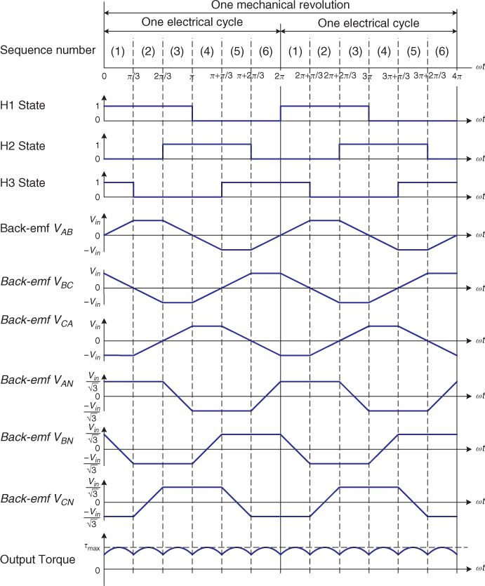
Table 4.2 States of Hall Sensors and Power Switches for Rotating Motor in Clockwise Direction
 |
Table 4.3 States of Hall Sensors and Power Switches for Rotating Motor in Counterclockwise Direction
 |
4.4.1.3 BLDC Motor Control
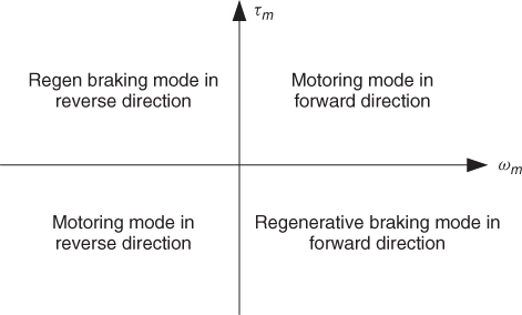
Since the propulsion motor in an HEV/EV needs to be operated in four quadrants, as shown in Fig. 4.40, the BLDC motor control tasks include determining the rotating direction, maintaining the demand torque, and regulating motor speed. The rotation direction of the BLDC motor can be easily controlled by changing the sequence of turning the power switches on and off based on the Hall sensor values. As an example, Table 4.2 gives the sequence for clockwise rotation and Table 4.3 for counterclockwise rotation based on the example motor and inverter circuit. However, it is a challenge to control the motor toque and regulate speed in HEV/EV applications. This is because the vehicle operates under various road and weather conditions as well as different driving styles; also the vehicle is accelerated and decelerated unpredictably. Such a load-varying nature demands higher fidelity and more accurate control strategies to deliver and maintain the required torque and speed. From the control system point of view, closed-loop control is the minimum to allow the motor to respond to the driver's request and load disturbance fast, accurately, and robustly. This section introduces a basic PID control strategy; there are advanced control strategies, such as adaptive control and model predictive control, capable of meeting the strict control performance requirements in emerging HVE/EV applications.
Figure 4.40 Four-quadrant operation of propulsion motor in HEV/EV.
A PID torque control diagram for an HEV/EV BLDC motor is shown in Fig. 4.41, where the input ![]() is the required torque from the vehicle controller, calculated based on the state of charge of the battery, engine speed, and position of the acceleration pedal or brake pedal. This required torque is then compared with the t-w characteristic curve at the present condition to ensure it within the motor's capacity; otherwise the torque will be saturated to the maximum torque of the motor. The processed
is the required torque from the vehicle controller, calculated based on the state of charge of the battery, engine speed, and position of the acceleration pedal or brake pedal. This required torque is then compared with the t-w characteristic curve at the present condition to ensure it within the motor's capacity; otherwise the torque will be saturated to the maximum torque of the motor. The processed ![]() is then converted to the required stator current
is then converted to the required stator current ![]() based on equation (4.75), and the required stator current is further limited within the maximum allowable current to set the desired stator current
based on equation (4.75), and the required stator current is further limited within the maximum allowable current to set the desired stator current ![]() . The error eI(k) between the desired stator current
. The error eI(k) between the desired stator current ![]() and the actual measured stator current Iactual feeds to the PID controller, which computes the corrective action Δu(k) from the following equation to PWM ratio which sent to three-phase inverter to produce the expected phase current for the BLDC motor. The on–off turning sequence of the power switches is based on the actual rotor position measured by the Hall sensor and the desired rotating direction of the BLDC motor:
and the actual measured stator current Iactual feeds to the PID controller, which computes the corrective action Δu(k) from the following equation to PWM ratio which sent to three-phase inverter to produce the expected phase current for the BLDC motor. The on–off turning sequence of the power switches is based on the actual rotor position measured by the Hall sensor and the desired rotating direction of the BLDC motor:
4.80 ![]()
where kp = K, ki = K/Ti, and kd = K · Td are called the proportional, integral, and derivative gain, respectively, and Ts is the sampling period. For the detailed PID controller design and analysis, the interested reader is referred to ![]() strom and Hägglund (1995).
strom and Hägglund (1995).
Figure 4.41 PID control diagram of BLDC motor for HEV/EV applications.

4.4.1.4 BLDC Motor Torque–Speed Characteristics and Typical Technical Parameters
As is well known, a key point to improve HEV/EV performance is to use a propulsion motor that matches with the characteristics of the battery system. From equations (4.75, 4.76, 4.77), we have the torque–speed characteristic curve shown in Fig. 4.42a. In HEV/EV applications, the torque is normally specified as applicable torque–speed characteristics with the constant-torque zone and constant-power zone shown in Fig. 4.42b. In the constant-torque zone, the output torque remains constant up to the rated speed, and once the motor speed is beyond the rated speed, the output torque starts dropping and is limited by the rated power. The maximum operating speed of the BLDC motor can be as high as double the rated speed. In practical HEV/EV system design, the motor is principally sized based on the required peak torque, RMS torque, and operating speed range. Table 4.4 gives typical parameters of the BLDC motor in HEV/EV applications.
Figure 4.42 Torque–speed characteristics of BLDC motor for HEV/EV applications.

Table 4.4 Typical Technical Specification Parameters of BLDC Motor for HEV/EV Application
 |
4.4.1.5 Sensorless BLDC Motor Control
From the preceding discussion, we know that a BLDC motor drive generally uses Hall sensors that provide rotor position information with a controller for synchronization. Hall sensors are costly and additional wiring is necessary, which may lower the vehicle system's reliability and durability. Since the 1980s, sensorless BLDC motor control technologies have been developed so the material cost can be reduced while meeting performance requirements.
Sensorless BLDC motor control is based on the relationship between the phase back EMF and the rotor position when the permanent magnet rotor is rotating; in other words, the rotor position can be detected by the measured phase back EMF so the synchronized phase commutations can be implemented without using physical position sensors.
The key technique implementing sensorless BLDC motor control is to effectively detect rotor position under different working conditions based on stator current and voltage. Various methods have been explored to improve system performance, including the extended Kalman filter state estimator, robust state observer, and artificial intelligent–based rotor position estimation methods such as fuzzy logic and artificial neural network.
4.4.2 AC Induction Motor and Control
The induction motor is widely accepted as a propulsion motor in HEV/EV applications due to lower cost, less maintenance, and longer lifetime. Since induction motors require an AC supply, they might seem unsuitable for the DC source of HEV/EV applications; however, nowadays AC can be easily inverted from a DC source with modern power electronics. The two common types of induction motor are based on the rotor structure: wound and squirrel cage. Three-phase squirrel cage induction motors are normally used in the lower end HEV/EV systems due to their rigidity and construction simplicity.
4.4.2.1 Basic Principle of AC Induction Motor Operation
All three-phase induction motors have same stator, consisting of three-phase windings distributed in the stator slots, displaced by 120° from each other. These stator windings produce the rotating magnetic field. A typical squirrel cage rotor consists of a series of conductive bars welded together at either end forming the short-circuit windings shown in Fig. 4.43.
Figure 4.43 Typical structure of squirrel cage rotor of AC induction motor.

As we know, a balanced three-phase sinusoidal current flowing through the stator establishes a constant rotating magnetic field with synchronous speed ωs = 2ω/p, where p is the number of magnetic poles created by the stator winding and ω is the angular frequency (rad/s) of the three-phase voltage applied to the stator. The rotating magnetic field intersects the rotor conductors at slip speed ωslip, inducing a corresponding EMF which causes current to flow in the short-circuit windings. The slip speed is the differential speed between the synchronous speed ωs of the rotating magnetic field and the rotor spinning speed, ωslip = ωs − ωr. Although the slip speed ωslip is a very important variable of the induction motor, the relationship between slip speed and synchronous speed, or slip, is most used in induction motor analysis. Slip s is defined as
4.81 ![]()
The phase equivalent circuit of an induction AC motor at steady state is shown in Fig. 4.44a, where ![]() is the supply voltage, Rs and Lsl are the resistance and leakage inductance of the stator windings, Lm is magnetic inductance, Rr and Lrl are the resistance and leakage inductance of the rotor windings, and Rr[(1 − s)/s] represents the developed torque.
is the supply voltage, Rs and Lsl are the resistance and leakage inductance of the stator windings, Lm is magnetic inductance, Rr and Lrl are the resistance and leakage inductance of the rotor windings, and Rr[(1 − s)/s] represents the developed torque.
Figure 4.44 Equivalent circuit of induction motor at steady state.

The equivalent circuit of Fig. 4.44a can be simplified as the circuit shown in Fig. 4.44b from Thevenin's theorem, where
4.82 
Thus,
4.83 ![]()
Since ωsLm ![]() ωsLsl, ωsLm
ωsLsl, ωsLm ![]() Rs,
Rs,
4.84 ![]()
from the Thevenin equivalent circuit of Fig. 4.44b, the rotor current is solved as

Since the absorbed electric power of the rotor is ![]() , which is equal to the output mechanical power Pme = τd · ωm = τe · ωr, the torque–speed relationship of the AC induction motor can be obtained as
, which is equal to the output mechanical power Pme = τd · ωm = τe · ωr, the torque–speed relationship of the AC induction motor can be obtained as
4.87 
where τe is the produced electromagnetic torque (Nm), ωr is the electrical angular speed (rad/s) of the rotor, τd is the developed mechanical torque (Nm) at the shaft, p is the number of magnetic poles created by the stator winding, Vs is the phase stator voltage, and f is the frequency (Hz) of the input voltage.
If the motor speed is represented by n in terms of RPM (revolutions per minute), then n = (60/2π)ωr; thus, the motor speed n can be expressed as
4.88 ![]()
From equation (4.87), we have the toque–speed characteristic curve of an induction motor illustrated in Fig. 4.45.
Figure 4.45 Torque–speed characteristics of induction motor.

4.4.2.2 Controls of AC Induction Motor
The torque–speed relationship equation (4.88) implies the following three ways to control the torque and speed of a squirrel cage induction motor:
From previous discussion, we know that the induction motor is singly excited and the rotor field is induced by the stator field; in other words, compared with DC or BLDC motors, the stator and rotor magnetic fields of the induction motor are not fixed orthogonal to one another. As we know, the developed torque of a DC motor can be expressed by the equation
where If is the field current that generates the field flux linkage and Ia is the armature current that generates the armature flux linkage. These two flux linkages are naturally orthogonal in a DC motor so it is easy to be controlled and has fast transient response.
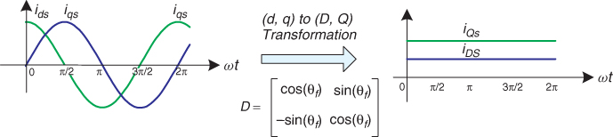
Vector control of an induction motor is the process of decoupling the stator current to a vector with two orthogonal components: air-gap flux current, or d axis ids, and torque current, or q axis iqs. It can be implemented by two transformations: first transforming three-phase stationary reference frame variables (as–bs–cs) into two-phase stationary reference frame orthogonal variables (ds, qs) and then synchronously rotating the reference frame variables (D, Q), or the DC quantities.
Assume that ias, ibs, and ics are the instantaneous balanced three-phase stator currents:
4.90 ![]()
This three-phase stationary reference frame (a, b, c) can be transformed into the two-phase stationary reference frame (d, q), shown in Fig. 4.46a, as

where i0s is the zero-sequence component making the matrix invertible so the two frames can be one-to-one transformed. This transformation can be applied to all quantities of an induction motor, including the phase currents, voltages, and flux linkages.
Figure 4.46 Stationary frame three-phase (a, b, c) to two-phase orthogonal (d, q) axes transformation.

Ignoring the zero-sequence component and setting θ = 0, that is, the qs-axis is aligned with the as-axis, the transformation relation equation (4.91) is simplified to
4.92 
Thus, (a, b, c) to (d, q) transforms a three-phase time-varying system into a two-phase time-varying system where the two variables are orthogonal. As shown in Fig. 4.46c, the d and q components in the two-phase stationary reference frame are still AC signals.
In vector control, all quantities must be stated in the same reference frame. Since the components ids and iqs depend on time and speed, the stationary reference frame is not suitable for the control process. To convert these two orthogonal AC signals to DC quantities, these components must be transformed from the stationary frame to the synchronous D, Q frame that rotates at the same speed as the angular frequency of the phase current by the following transformation:
4.93 ![]()
The D and Q components in equation (4.93) actually rotate at the synchronous speed ωs with respect to the (d, q) axes at the angle θf = ωst, which is equivalent to mounting the two-phase (d, q) windings on the hypothetical frame rotating at the synchronous speed, resulting in conversion of the sinusoidally varying waveforms to the DC vector shown in Fig. 4.47. After getting these DC quantities, each component of the DC vector can be independently controlled to generate the desired torque, which mimics the torque equation of a DC motor.
Figure 4.47 Stationary frame (d, q) to synchronous frame (D, Q) transformation.
By applying the above transformations, the voltage and flux linkage equations of the stator and rotor as well as electromagnetic torque of an induction motor in the synchronous frame can be written as follows:
4.94 ![]()
4.95 ![]()
4.96 ![]()
4.97 ![]()
4.98 ![]()
4.99 ![]()
4.100 ![]()
4.101 ![]()
4.102 ![]()
4.103 ![]()
where
vQs = stator quadrature-axis voltage (V)
vDs = stator direct-axis voltage (V)
vQr = rotor quadrature-axis voltage (V)
vDr = rotor direct-axis voltage (V)
iQs = stator quadrature-axis current (A)
iDs = stator direct-axis current (A)
iQr = rotor quadrature-axis current (A)
iDr = rotor direct-axis current (A)
ΨQs = stator quadrature-axis flux linkage (Wb)
ΨDs = stator direct-axis flux linkage (Wb)
ΨQr = rotor quadrature-axis flux linkage (Wb)
ΨDr = rotor direct-axis flux linkage (Wb)
Rs = stator phase resistance (Ω)
Rr = rotor phase resistance (Ω)
Ls = stator phase inductance (H)
Lr = rotor phase inductance (H)
Lm = magnetizing inductance (H)
ωs = synchronous speed (rad/s)
ωr = electrical rotor speed (rad/s)
ωm = mechanical rotor speed (rad/s)
p = number of pole
τd = developed torque (Nm)
τload = load torque (Nm)
τloss = lumped loss torque (Nm)
J = rotor inertia (kg· m2)
The above vector or field-oriented control method was invented in the early 1970s and enables an induction motor to be controlled like a separately excited DC motor. Vector control brought a renaissance to the performance control of AC drives. With advances in modern power electronics and microelectronics as well as development of control techniques, vector control has been accepted as the standard in AC drives and has been widely applied to HEV/EV propulsion systems as well.
An implementation block diagram of the vector control is shown in Fig. 4.48 for HEV/EV applications. In this example, once the position signal of the acceleration or brake pedal is received, the vehicle controller calculates the demand torque based on the vehicle speed, DC link voltage, and motor speed and sends a torque request to the motor controller. The motor control then calculates the desired stator direct-axis current ![]() and quadrature-axis current
and quadrature-axis current ![]() in response to the corresponding command
in response to the corresponding command ![]() from the vehicle controller. These two desired current values are compared to the actual stator direct-axis current iDs and quadrature-axis current iQs. The errors between the desired and actual currents,
from the vehicle controller. These two desired current values are compared to the actual stator direct-axis current iDs and quadrature-axis current iQs. The errors between the desired and actual currents, ![]() and
and ![]() , are fed to the PID controller or an advanced controller to calculate the control requests
, are fed to the PID controller or an advanced controller to calculate the control requests ![]() and
and ![]() . The motor controller makes use of two stages of inverse transformation to generate three-phase request signals
. The motor controller makes use of two stages of inverse transformation to generate three-phase request signals ![]() , and
, and ![]() to produce a PWM switching sequence for the three-phase inverter. At the same time, the measured rotor flux position signal θf is sent by the inverse transformation block to ensure correct alignment between current
to produce a PWM switching sequence for the three-phase inverter. At the same time, the measured rotor flux position signal θf is sent by the inverse transformation block to ensure correct alignment between current ![]() and the rotor flux ΨDr and perpendicular to current
and the rotor flux ΨDr and perpendicular to current ![]() . On the other hand, the inverter generates currents ia, ib, and ic in response to the corresponding command currents
. On the other hand, the inverter generates currents ia, ib, and ic in response to the corresponding command currents ![]() , and
, and ![]() from the motor controller. The measured terminal currents ia, ib, and ic are converted to ids and iqs through the forward three–two orthogonal phase transformation. They are further converted to iDs and iQs components by the stationary frame–synchronous frame transformation with the measured rotor flux position signal θf.
from the motor controller. The measured terminal currents ia, ib, and ic are converted to ids and iqs through the forward three–two orthogonal phase transformation. They are further converted to iDs and iQs components by the stationary frame–synchronous frame transformation with the measured rotor flux position signal θf.
Figure 4.48 Block diagram of induction motor vector control for HEV/EV applications.

In general, the vector control technique uses the dynamic equivalent circuit of the induction motor to decouple the stator current into two perpendicular components—one generating the magnetic field and the other producing torque—so they can be independently controlled as a DC drive. Progress in power electronics, microelectronics, and control techniques has substantially supported the application of induction motors to high-performance drives.
4.5 Plug-In Battery Charger Design
Plug-in hybrid electric vehicles (PHEVs) and BEVs have been and continue to be developed. To charge the battery of a PHEV/BEV, a high-efficiency charger is needed. The Electric Power Research Institute defined the following three charging levels:
4.5.1 Basic Configuration of PHEV/BEV Battery Charger
No matter what level the plug-in charger is, the operation principle and basic system configuration are the same. The charger consists of an EMI filter, a full-wave rectifier, in-rush current protection, power factor correction (PFC), and a DC-DC-converter. The architecture of a PHEV/BEV battery charger is illustrated in Fig. 4.49.
Figure 4.49 Architecture of PHEV/BEV battery charger.

There are many semiconductor power switches in a PHEV/BEV battery charger, and the switch-mode operation is the source of the EMI produced. To meet the EMI requirements, standards, and national codes, special measures must be taken to limit the EMI level. The most cost-effective way is to install an EMI filter at the AC input port.
Since the discharged capacitor initially approaches the short-circuit state when voltage is applied to it, a precharge resistor is necessary to limit in-rush current during power up. Once the precharge is completed, the bypass switch shorts the precharge resistor to eliminate undesired power loss. The function of the rectifier is to transfer sinusoidal AC voltage into DC voltage, and the most common circuit is the full-bridge rectifier. Any type of power electronics, such as diodes, thyristors, and MOSFETs, can perform the transformation; however, since it is not necessary to control the output voltage, diodes are the easiest and most economical components to implement the function. The rectifier, shown in Fig. 4.49, is composed of diodes D6, D7, D8, and D9. When the input AC is positive, D6 and D9 are on and D7 and D8 are off, while when the input AC is negative, D6 and D9 are off and D7 and D8 are on. In most cases, a filter capacitor is placed in parallel to the rectifier output to improve the quality of the DC voltage. The waveforms of a full-bridge rectifier are shown in Fig. 4.50.
Figure 4.50 Voltage waveforms of full-bridge rectifier with filter capacitor.

To minimize harmonic distortion and improve the power factor, most PHEV/BEV battery chargers incorporate PFC devices. After the PFC, the DC–DC converter finally converts the rectified DC voltage to the desired DC voltage to charge the battery based on the control command from the battery system.
4.5.2 Power Factor and Correcting Techniques
As a means of minimizing harmonic distortion and improving the power factor, PFC is an important technique applied to PHEV/BEV battery chargers. The power factor is defined as the ratio of the real power to the apparent power by the equation
4.104 ![]()
where P is the real power (W) and S is apparent power (VA).
If we assume that both current and voltage waveforms are ideal sinusoidal, the three power components real power P, apparent power S, and reactive power Q in volt-amperes form the right triangle shown in Fig. 4.51. The relationship among them is given as
4.105 ![]()
4.106 ![]()
where ϕ is the angle between the input voltage and current and is defined as the phase lag/lead angle or displacement angle in the ideal sinusoidal waveform.
Figure 4.51 AC power triangle.

If we consider the case of a PHEV/BEV charger where the input voltage stays undistorted and the current waveform is periodic nonsinusoidal, the real power and apparent power are
4.107 ![]()
where I1, RMS is the RMS (root-mean-square) value of the fundamental frequency component of the current. As a nonsinusoidal waveform contains harmonic components in addition to the fundamental frequency, a distortion factor kd is further defined to quantify the impact of harmonic components on the real power:
4.108 ![]()
Applying the Fourier transform to the current, the RMS value of the current can be obtained as
4.109 ![]()
where I0 is the DC component of the current and I0 = 0 because the distorted current is with a pure AC waveform, I1, RMS is the RMS value of the fundamental component of the current, and I2, RMS ![]() In, RMS are the RMS values of the harmonic components of the current.
In, RMS are the RMS values of the harmonic components of the current.
Figure 4.52 shows the input current waveform of a full-bridge rectifier with filter capacitor and without a PFC corresponding with Fig. 4.50c. Since the typical rectifier only charges the capacitor when the input voltage is greater than the voltage on the capacitor, the input current flows only near the peak input voltage; therefore, the value of I1, RMS is very small, which results in an actual power factor that is generally less than 0.5:
4.110 ![]()
There are many methods that can improve the power factor; however, the most common technique used in plug-in chargers is to apply a PFC in the circuit shown in Fig. 4.49. The objective of placing a PFC is to extend the current conduction angle β to 180°, while the operation principle is similar to that of the boost DC–DC converter shown in Fig. 4.19. By means of inductance LPFC and switching Q5 with higher frequency, the input AC waveform closely tracks the rectified AC voltage shown in Fig. 4.53.
Figure 4.52 Input voltage and current of full-bridge rectifier with filter capacitor.

Figure 4.53 Principle of PFC operation.

4.5.3 Controls of Plug-In Charger
The PHEV/BEV battery system is normally charged through two stages of operation: constant-current mode and constant-voltage mode, as shown in Fig. 4.54. The switching point of the charging mode is controlled by the maximum charging voltage sent by the battery system controller, and the maximum charging voltage is determined by the operation temperature and desired battery SOC to be charged to. To implement the constant-current and constant-voltage operation, the charging control scheme normally consists of two closed loops: a voltage loop and a current loop. A common charging control scheme is shown in Fig. 4.55, where the voltage loop is placed as an outer loop and the PI controller generates the desired current to the inner loop based on the difference between the desired charging voltage and actual battery voltage. The PI controller cooperates with a saturation block and an anti-windup block to limit the generated current reference. In the current loop, the difference between the generated desired current and actual charging current is fed to the PI controller to generate the PWM signal that operates the corresponding power switches on or off to obtain the desired battery charging curve.
Figure 4.54 Required charging process of PHEV/BEV battery.
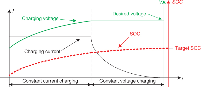
Figure 4.55 PHEV/BEV charging control scheme.

References
Moham, N., Undeland, T. P., and Robbins, W. P. Power Electronics—Converters, Applications, and Design, 3rd ed. Wiley, Hoboken, NJ, 2003.
Rashid, M. H. Power Electronics Circuits, Devices, and Applications, 3rd ed. Prentice-Hall of India, New Delhi, 2008.
Erickson, R. W., and Maksimovic, D. Fundamentals of Power Electronics, 2nd ed. Springer, New York, NY, 2001.
Astrom, K., and Hägglund T. PID Controllers: Theory, Design and Tuning, 2nd ed. Instrument Society of America, Research Triangle Park, NC, 1995.