
Terahertz Spectroscopy and Imaging
School of Electronic and Electrical Engineering
University of Leeds, Leeds LS2 9JT, U.K.
1. Introduction
The terahertz (THz) region (0.3–10 THz) of the electromagnetic spectrum spans the frequency range between the infrared and millimeter/microwave, as illustrated in Fig. 1. Historically this region has not been fully exploited owing to the very limited number of suitable (in particular, coherent) radiation sources and detectors that have been available. In recent years,1 outstanding progress has been made in developing THz components and systems. Highlights include the fabrication of the first THz quantum cascade laser,2 together with the commercialization of THz spectroscopy and imaging systems based on femtosecond-laser technology,3 notably for non-destructive testing in the pharmaceutical industry (for example, investigating polymorphic transformations, and drug distributions in tablets4). Further, three years ago an ultra-broadband THz spectroscopy system was proposed, making use of photoconductive emitters in a reflection geometry. This offered a bandwidth in excess of 20 THz for spectroscopy applications,5 and its performance was demonstrated through measurements of the absorption of polycrystalline adenosine.1 Good agreement was obtained with spectra acquired using the complementary technologies of Fourier-transform infrared, Raman, and neutron inelastic spectroscopy.
Despite these exciting developments, when the previous conference treatise1 reviewed THz technology, the field of THz imaging and spectroscopy was still in its infancy: extensive research was needed on the basic interactions of THz radiation with materials. Even so, a diverse range of applications had been identified across the physical, biological and medical sciences, including medical and dental imaging, the detection of concealed explosives and drugs, biomedical spectroscopy, atmospheric sensing, process monitoring, non-destructive testing of composite materials, diagnostic testing, high-bandwidth communications, astronomy, and condensed matter physics, inter alia.

Figure 1. Schematic diagram showing the electromagnetic spectrum, and illustrating the “THz gap” for which there has been, until recently, a lack of convenient solid-state sources and detectors.
Over the past three years, the field of THz spectroscopy and imaging has undergone extremely rapid growth, with major developments being seen in THz components, THz systems and potential application areas. To give just three examples:
- THz spectroscopy is being considered by security agencies around the world as a potential technique for identifying drugs-of-abuse and explosives;
- on-chip THz systems have been extensively developed, and offer an exciting prospect both for biomedical sensing with femtomole sensitivity, and the detailed study of condensed matter systems at cryogenic temperatures;
- THz quantum cascade lasers have been demonstrated to operate at frequencies below 2 THz, and at temperatures above 160 K. They are also being incorporated into THz imaging systems.
Here, we discuss two of these developments in greater detail: the development of on-chip THz systems, and the applications of THz spectroscopy for studying drugs-of-abuse and explosives; the latest developments in the field of THz quantum cascade lasers are discussed elsewhere in this volume. We conclude this chapter by considering just a few of the possible developments that may be seen in the field of THz spectroscopy and imaging over the next three years and beyond.
2. Broadband THz spectroscopy of drugs-of-abuse and explosives
Figure 2 shows an experimental configuration allowing THz radiation with frequency components over 20 THz to be obtained using a biased and asymmetrically excited GaAs photoconductive emitter. Its maximum useful bandwidth exceeds that seen in most THz systems based on photoconductive emitters, which are generally limited to ~4 THz.
In brief, the emitter comprises two vacuum-evaporated NiCr/Au electrodes separated by a 0.4 mm gap, deposited on a low-temperature-grown (LT) GaAs layer. We chose LT-GaAs because it provides a short photocarrier recombination lifetime (0.4 ps in this case), together with both high resistivity and high carrier mobility. A bias voltage of ±120 V, modulated at 31 kHz, was applied across the emitter. A pulsed Ti:sapphire laser of 300 mW average power (12 fs pulse width, 800 nm centre wavelength, and 76 MHz repetition rate) was focused to a 40 μm spot diameter on the edge of one of the two NiCr/Au electrodes of the LT-GaAs emitter, to generate THz pulses. In contrast to previous experiments, where the THz radiation was collected after being transmitted through the GaAs substrate, THz radiation was collected, in this case, in the same direction as the reflected pump laser beam. As a result, the absorption and dispersion of the THz pulses in the GaAs substrate were minimized. The emitted THz pulses were collimated and focused onto the sample by a pair of parabolic mirrors. The transmitted THz pulse was then collected and focused using another pair of parabolic mirrors onto a 20 μm-thick (110) ZnTe crystal glued onto a 1 mm-thick wedged (100) ZnTe crystal for electro-optic detection. A variable delay stage provided the time delay between the THz and probe pulses, and the system had a spectral resolution of 75 GHz (2.5 cm−1). Using a lock-in detection scheme referenced to the frequency of the bias across the GaAs emitter, a signal-to-noise ratio of over 1000 was achieved. The apparatus was enclosed in a vacuum-tight box, and purged with dry nitrogen gas to reduce the effects of water vapor absorption.
Figure 3 shows absorption spectra observed at room temperature with this system for pellets of the explosives 2,4,6-trinitrotoluene (TNT), hexahydro-1,3,5-trinitro-1,3,5-triazine (RDX), and pentaerythritol tetranitrate (PETN),6 diluted in a 20% weight-to-weight ratio with the inert matrix PTFE. Absorption peaks in the 0.3−3 THz region can be easily seen and correspond well with previously reported data.7 Significantly, absorption bands can also be seen in the 3−5.5 THz region, with the bandwidth of the system in this case being limited by the PTFE phonon resonance at 6 THz. The higher frequency absorption is particularly prominent in the spectra of TNT, where the bands above 3 THz are much more intense than those in the 0.1−3 THz region. This is important, because the lower frequency peaks are difficult to observe above the background noise at low concentrations of explosive.

Figure 2. Schematic diagram illustrating a femtosecond laser-based ultrabroad-band THz spectroscopy system.

Figure 3. THz absorption spectra of TNT, RDX and PETN, diluted in a 20% weight-to-weight ratio with PTFE. Spectra for TNT and RDX are offset for clarity.6
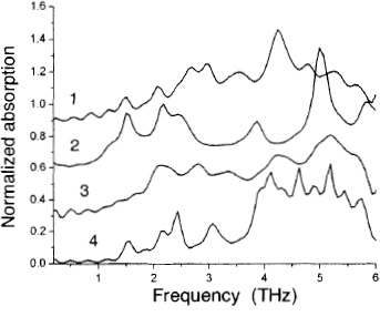
Figure 4. THz spectra of a number of drugs-of-abuse: (1) cocaine hydrochloride 25%; (2) cocaine free base 100%; (3) morphine sulfate pentahydrate 25%; and (4) ephedrine hydrochloride 12.5%. The spectra are offset for clarity; the percentages refer to weight-to-weight ratios of drug to PTFE matrix in the pellets, chosen to optimize the absorption spectra. There are marked differences in spectral features, even for similar molecular structures.6
Figure 4 shows spectra for three drugs-of-abuse: cocaine hydrochloride (Sigma-Aldrich lot no: 123k1339); cocaine free base (lot no: 044k0854); and morphine sulfate pentahydrate (lot no: 044k0736); together with ephedrine hydrochloride (lot no: 12019cu-034) that, although not classified as a drug-of-abuse, can act as a precursor to amphetamine and ecstasy. By mixing the drug samples with PTFE and optimizing the concentrations, good definition of spectral peaks was obtained over the full bandwidth of the spectrometer (no difference in the spectral positions of absorption features was observed for different concentrations). It is notable that large differences in spectra can be seen for small differences in molecular structure (for example, between cocaine free base and cocaine hydrochloride).
These data demonstrate that broadband THz spectroscopy can be used to analyze materials of security relevance, although considerable further development is needed before such technology can be used in real-life applications. In particular, there is a need to demonstrate a similar discrimination in “street” samples, which are likely to contain a range of contaminants.
3. The development of on-chip THz systems
The majority of THz spectroscopy, to date, has been undertaken using free-space reflection or transmission measurements, in which THz radiation is generated in free space by near-infrared excitation of photoconductive or electro-optic emitters, focused onto a sample using off-axis parabolic mirrors, and subsequently detected using either photoconductive or electro-optic detectors, in schemes similar to that presented in Section 2 above. Whilst this has been enormously successful in allowing a broad range of applications to be investigated, it has some clear limitations. For example, spectral resolution typically exceeds 20 GHz – too large to obtain the required peak resolution for many applications, and too much material is often required for promising areas such as the development of biosensors.
An extremely promising alternative is to generate and detect THz radiation on-chip.8 A similar photoconductive excitation and detection mechanism is used as in the free-space systems, but the excited THz pulses are now directly coupled into lithographically defined transmission lines, which are formed in either microstrip or strip-line/coplanar geometries.

Figure 5. Schematic diagram (inset) of an on-chip guided wave THz system. A pulse of THz radiation is emitted by photoconductive antennae at position 1 or 2, and transmitted along the strip-line to a detector at position 3. Band-stop filters, in this case 82 μm and 194 μm long (optical photograph), remove selected frequencies from the transmitted THz pulse.
A recent on-chip system is illustrated in Fig. 5.9 Terahertz radiation is generated with a femtosecond laser pulse by exciting a photoconductive emitter (marked 1, Fig. 5) deposited on LT-GaAs. This excites a THz transient response, which propagates along the transmission line (a 4 mm-long strip-line in this case), and is detected in a photoconductive detector (marked 3, Fig. 5), which is gated by part of the initial femtosecond laser pulse. Figure 6 shows typical data when a ~ps duration pulse has been excited in an on-chip device, and then detected, both before and after propagation down 4 mm of microstrip. In this case, the transmitted pulse shows a ringing associated with the presence of a band-stop filter attached to the microstrip line (see Fig. 5). Fourier transformation of the acquired time-domain spectra then allows the broadband transmitted THz pulse to be determined in the frequency domain, giving similar data to that shown in Fig. 3, albeit over a narrower bandwidth.
Low-loss materials, for example benzocyclobutene (BCB) or PTFE, can be used as appropriate dielectrics in such microstrip geometries. Signal conductors are typically patterned as gold tracks that extend over several mm on the dielectric surface, before terminating at a photoconductive emitter/detector regions. In order to use on-chip systems for useful spectroscopy, the evanescent field lines around the transmission line can be exploited. To increase sensitivity, filter structures can be fabricated in the waveguide whose resonant frequency is sensitively dependent on the local dielectric environment around the filter. By monitoring detuning of the filter when overlaid materials are deposited, one can determine an unknown dielectric's permittivity at the filter frequency (provided the thickness can also be measured, which is a limitation of this technique). Several filter geometries have been studied for this application, including bandpass,8 bandstop filters,9 and ring resonators.10

Figure 6. Typical pulse data obtained in the microstrip system shown in Fig. 5, with BCB used as the dielectric. Incident (before transmission down microstrip-line) and transmitted pulses (after transmission through the filter) are both shown.
Typical results for an overlaid dielectric material on dual-bandstop filter systems are shown in Fig. 7, where the frequency shift of each filter depends critically on the different thicknesses of dielectric material deposited. These measurements of frequency shift have been compared with full 3D electromagnetic simulations11 and, using a value for relative permittivity εr that had been independently measured using a free-space THz time domain spectroscopy system, good agreement is obtained with the frequency shifts found experimentally.
A significant feature of on-chip systems is that the sample volume required is miniscule compared with the free-space techniques, typically a factor of several hundred lower. Furthermore, since reflected pulses can be designed out of the system (by choosing several mm-long probe arms and a microstrip signal conductor), the frequency resolution of an on-chip system has the potential to exceed free-space systems (where resolution is typically limited by back-reflections from sample, emitter, and detector surfaces). Indeed, a resolution of 2 GHz has recently been demonstrated in on-chip Fourier transformed data, limited by the resolution of linear translation in time-delay stages.

Figure 7. Fourier transforms of pulsed transmission data obtained from a two bandstop filter array, before (solid) and after (dashed) the deposition of a circular film of dielectric material (Shipley S1813 photoresist) around the higher frequency filter (600 GHz), as shown in the small inset. A resulting shift to lower frequencies in the response of the 600 GHz filter can be seen, leaving the centre frequency of the 260 GHz filter and its third harmonic unaffected. Insets show response of the 260 GHz filter (a) and 600 GHz filter (b) to different thickness of S1813 dielectric. In both insets, squares represent experimental data, lines are simulations using εr = 2.75 (solid) obtained from free-space measurement for S1813 at 600 GHz, εr = 2 (dashed, lower) and εr = 3.5 (dashed, upper).
In contrast to free-space propagation, the potential of THz guided wave devices for imaging has not yet been explored. Evanescent field imaging is a method common in the GHz range,12 in which samples are scanned in the region of an evanescent electric field that extends above a planar microwave circuit. The transmission parameters of the circuit are affected by this perturbation, and these changes are recorded as the sample is scanned in a 2D plane in order to give a dielectric contrast map of the sample. The work on evanescent fields above planar THz filter systems described here offers a potential route to performing similar microscopic studies at THz frequencies.
A further advantage of on-chip systems is that it should be possible to undertake THz spectroscopy on condensed matter physics based systems, such as high mobility two-dimensional electron gases in the quantum Hall regime. In particular, it offers a far greater interaction length with the device under test compared with free-space based techniques. A key requirement for this type of investigation is that the micro-strip geometry should operate successfully not only at room temperature, but also at cryogenic temperatures. Figure 8 demonstrates that this can be successfully accomplished,13 with the detected pulse at 4 K actually narrowing compared to the measured pulse at 290 K. This technology thus opens the pathway for high-frequency (THz) studies of the dynamic conductivity in solid-state systems at cryogenic temperatures, and in high magnetic fields.
4. Future directions
Outstanding progress has been made, over the last three years, in developing THz components and systems. In particular, intense international interest has arisen in the prospects of designing THz spectroscopy and imaging systems that can detect materials of security interest. In parallel, there has been striking progress in the design of on-chip THz time domain spectroscopy systems, which offer a 10x higher frequency resolution, and are sensitive to far smaller sample volumes. These may find potential applications as biochip DNA sensors or in the study of condensed matter physics systems.

Figure 8. Detected THz pulse along a microstrip line based on a BCB dielectric, and LT-GaAs photoconductive emitters and detectors.13 Narrowing of the pulse width is observed as T is lowered from 290 K to 4 K.
Despite this remarkable progress, there remain many key issues still to be resolved before the full impact of THz technology becomes clear over the next three years and beyond. These include:
- despite the immense progress seen in quantum cascade laser design, will spectroscopy and imaging systems be constructed that compete long-term with the already established commercial pulsed (femtosecond) systems?
- can the cost of commercial pulsed (femtosecond) spectroscopy and imaging systems be reduced to allow a greater market uptake? For example, can incorporation of 1.55 μm InP telecom technology, or the use of diode laser mixing schemes, supplant existing femtosecond laser technology?
- can on-chip THz systems demonstrate their true potential over free-space alternatives, especially for biomedical spectroscopy and condensed matter physics?
- will we see THz systems being used for security applications at airports, and will we see stand-off detection being implemented in real-life situations, or will such systems remain simply a fundamental research tool in vibrational spectroscopy?
- what are the real prospects for using THz radiation in medical and dental imaging applications today, given the initial demonstrations that were made over five years ago?
- what new applications may emerge?
- can realistic simulations be obtained of the THz vibrational modes of complex molecular crystal structures?
Much research still has to be undertaken, but there is clearly an exciting future for THz technology and its applications, which is set to continue over the next decade and beyond. From a fundamental viewpoint, it is anticipated that extensive research will be undertaken on THz interactions with condensed matter physics systems and nanostructures, with a range of new phenomena being revealed in a high-frequency regime that has hitherto been inaccessible to solid state researchers. As examples, the energy spacings in quantum dots, transit times in submicron transistors, phonon modes in nanostructures, and torsional modes in DNA are all expected to lie within the THz spectral range.
Acknowledgments
This work was supported by the U.K. Engineering and Physical Sciences Research Council (EPSRC), and Research Councils UK.
References
- S. Luryi, J. Xu, and A. Zaslavsky, eds., Future Trends in Microelectronics: The Nano, the Giga, and the Ultra, New York: Wiley, 2004.
- R. Köhler, A. Tredicucci, F. Beltram, et al., “Terahertz semiconductor-heterostructure laser,” Nature 417, 156 (2002).
- D. H. Auston, K. P. Cheung, and P. R. Smith. “Picosecond photoconducting Hertzian dipoles,” Appl. Phys. Lett. 45, 284 (1984).
- P. Taday, I. V. Bradley, D. D. Arnone, and M. Pepper, “Using terahertz pulse spectroscopy to study the crystalline structure of a drug: A case study of the polymorphs of ranitidine hydrochloride.” J. Pharm. Science 92, 831 (2003).
- Y. C. Shen, P. C. Upadhya, E. H. Linfield, H. E. Beere, and A. G. Davies, “Ultrabroadband terahertz radiation from low-temperature-grown GaAs photoconductive emitters.” Appl. Phys. Lett. 83, 3117 (2003).
- A. Burnett, W. Fan, P. Upadhya, et al., “Analysis of drugs of abuse and explosives using terahertz time domain and Raman spectroscopy”, Proc SPIE 6120, 155(2006).
- Y. C. Shen, T. Lo, P. F. Taday, B. E. Cole, W. R. Tribe, and M. C. Kemp, “Detection and identification of explosives using terahertz pulsed spectroscopic imaging,” Appl. Phys. Lett. 86, 24116 (2005).
- M. Nagel, P. Haring-Bolivar, M. Brucherseifer, H. Kurz, A. Bosserhoff, and R. Büttner, “Integrated THz technology for label-free genetic diagnostics.” Appl. Phys. Lett. 80, 154 (2002).
- J. Cunningham, C. D. Wood, A. G. Davies, K. C. Tiang, P. A. Tosch, E. H. Linfield, and I. C. Hunter, “Multiple-frequency terahertz pulsed sensing of dielectric films,” Appl. Phys. Lett. 88, 071112 (2006).
- M. Nagel, F. Richter, P. Haring-Bolivar and H. Kurz, “A functionalized THZ sensor for marker-free DNA analysis,” Phys. Med Biol. 48, 3625 (2003).
- C. K. Tiang, J. Cunningham, C. D. Wood, I. C. Hunter, and A. G. Davies, “Electromagnetic simulation of terahertz frequency range filters for genetic sensing.” J. Appl. Phys. 100, 066105 (2006).
- M. Tabib-Azar, P. S. Pathak, and G. Ponchak, “Nondestructive super-resolution imaging of defects and nonuniformities in metals, semiconductors, dielectrics, composites, and plants using evanescent microwaves” Rev. Sci. Instrum. 70, 2783 (1999) and references therein.
- C. D. Wood, J. Cunningham, P. Upadhya, E. H. Linfield, I. C. Hunter, A. G. Davies, and M. Missous, “On-chip photoconductive excitation and detection of pulsed terahertz radiation at cryogenic temperatures,” Appl. Phys. Lett. 88, 142103 (2006).