
Chapter 7
Measurement of the Shielding Effectiveness
7.1. Introduction
The measurement of shielding effectiveness was one of the first applications of reverberation chambers devoted to electromagnetic compatibility [DEG 07,HAT 88, LEF 06].
Usually, shielding effectiveness is expressed in terms of an attenuation brought by a shield inserted between the electromagnetic disturbance source and the dedicated protected circuit. In the context of the measurement methods highlighted in this chapter, the circuit will be constituted by a field probe or by the loads at the ends of a cable or of a connector. This context has thus led us to subdivide the analysis into three parts, depending on whether our focus is the shielding protection of cables or connectors, the shielding protection of enclosures hosting electronic circuits, or the characterization of the attenuation brought by various shieldingmaterials.
The next sections of this chapter will develop these different aspects of shielding measurements. After suggesting in section 7.2 several definitions of the shielding effectiveness, section 7.3 tackles the question of the measurement of the effectiveness of shielded cables and connectors in reverberation chambers. Knowing that we aim at disturbances coming from RF emissions, the cable shields behave like wiring circuits immersed in the ideal random field distribution of the reverberationchamber.
The physical analysis detailed in section 7.3 leads to the search for a methodology enabling us to link the transfer impedance of a shielded cable to the attenuation deduced from the measurements carried out in reverberation chambers.This is a very important goal, when we know that below 1 GHz, the effectiveness of a shielded cable often comes from transfer impedance measurements, which are carried out on laboratory benches. Whereas above 1 GHz, the determination of the attenuation in reverberation chambers seems more appropriate to obtain reproducible results. This section concludes with an example taken from the measurements obtained on a short sample of a coaxial cable with an imperfect shield made up of a copper tube with a small aperture.
Section 7.4 is devoted to the measurement of the shielding effectiveness of enclosures in continuation of the previous analysis. The possible weakness of the shield is due to various electromagnetic leakages that take place on some parts of the metal box. In this context, the main interest of the test carried out in reverberation chambers is related to the properties of the random field distribution. Indeed, we have seen during the previous chapters that a test in reverberation chambers was similar to the radiation exposure of the device to randomly distributed incoming plane waves. Thus, this analogy lends itself quite well to characterization of the electromagnetic leakages, whose radiation pattern is unknown. The example of the attenuation given by a slotted cavity, will show that only one test gathers the main coupling phenomena.
Concluding this chapter, section 7.5 tackles the attenuation measurement of the shielding materials in reverberation chambers. Contrary to shielded cables, it is practically impossible to establish a link with the measurement methods of the attenuation, as it is recommended by some standards with the device under test inserted into a coaxial cell. After a brief description of the two measurement methods of the attenuation of materials commonly used in reverberation chambers,an example shows the interest brought by the method lying on the shunting of an aperture. This technique consists of successive measurements of the coupled electromagnetic field within a shielded enclosure with a rectangular aperture on one side containing a sample. Few experiments carried out on a conductive polymer sample show the continuity of the various frequency responses of the attenuation measurements successively produced in a TEM cell, in an anechoic chamber and in a reverberation chamber.
7.2. Definitions of the shielding effectiveness
Electromagnetic shielding consists of a barrier against the effect of the electromagnetic interferences, which may be more or less reduced according to the physical characteristics of the shield.
The term “barrier” implies that the shield provides significant attenuation to the electromagnetic disturbances located on the other side of the shield. This so-called primary interference may be a source of electric field, magnetic field, current orvoltage.
If the resulting interference collected after insertion of the shielding barrier and the primary interference source are expressed with the same physical unit, we use as a common definition of the shielding attenuation, the ratio between the interferences amplitudes collected before and after insertion of the shielding barrier.
The interference phenomena produced in the context of the tests carried out in reverberation chambers are generated with sinusoidal RF emissions. Therefore, the measurement of the shielding effectiveness will consist of evaluating the variations of the attenuation versus the frequency. Taking into account the important variations of measured interference levels on wide frequency bands we normally use a logarithmical scale for the attenuation which is displayed in decibels (dB).
Depending on whether we discuss the measurements of field, current, voltage or power, the previous definitions are transposed by the formulas below:
[7.1] 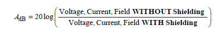
[7.2] 
The next sections will be devoted to the definitions that we need to use, in order to measure the shielding effectiveness of the cables and connectors, the shielded enclosures and the shielding materials.
7.2.1. Shielding effectiveness of cables and connectors
This section details the various definitions of the attenuation provided by shielded cables. However, we will not have any difficulty extending the physical principles of the definition to shielded connectors [CRA 88, DEG 07, MAR 00].
Usually, the shielding effectiveness of a cable is supported by the concept of transfer impedance [DEM 10]. The context is recounted in Figure 7.1, for a coaxial cable matched at both ends. The terminations are thus connected to resistances with values strictly similar to the characteristic impedance Zc of the cable.
With a suitable device, often made up of a concentric tube at the shield, we forma transmission line, in order to inject the current IS into the cable shield. This current generates voltages collected at both ends of the cable, which are noted later on asVc(0) and Vc(L0). Supplied by a RF generator under the angular frequency ω, and assuming that the wavelength λ of the signals remains much higher than the dimension of the cable L0, the current IS can be kept uniform with the longitudinal zvariable. The transfer impedance of the shielding, designated by the notation Zt, is then linked to previous parameters by equation [7.3]:
[7.3] ![]()
Figure 7.1. Reference device for the definition of Zt

Use of these equations involves that the transfer impedance provided by the shielded cable only depends on the physical parameters of the cable, like the shield construction, its diameter, electrical conductivity of the shielding material.
In the context of Figure 7.1. formula [7.1] of the shielding attenuation adopting the currents or voltages, can be established according to a convention where the current IS flows in the inner conductor. Thus, according to the termination impedances, the Vc’(0) and Vc’(L0) voltages take the respective expressions:
[7.4] ![]()
The AdB attenuation brought by the shielding then comes down to the following formulas:
[7.5] 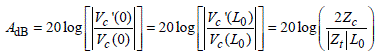
The use of absolute values is justified by the fact that the transfer impedance can have the properties of a complex number.
According to the use of this definition, the attenuation given by the shield involves other parameters that the shield characteristics only, such as the cable dimension and the load impedance.
If we attempt to divert the meaning of [7.1] and [7.2], by setting out that the attenuation A of the shielding is the ratio of the physical parameter which is collected by the shield on the resulting physical parameter collected by the cable,i.e.:
[7.6] 
The transcription of this definition for the example illustrated in Figure 7.1. leads to the ratio of the current IS, which is produced on the shield on the resulting currents Ic(0) and Ic(L0). These currents are collected on the terminations loads.Converted into dB, the attenuation is expressed as:
[7.7] 
We reach a result very similar to expression [7.5]. However, this does not mean that in the general case the two definitions are equivalent.
If we imagine the device under test in Figure 7.1 exposed to an electromagnetic wave, coming from a neighboring transmitting antenna, using definitions [7.1] and [7.2] is absurd.
Indeed, the only way of collecting the energy without the shield would be to consider the inner conductor as a receiving antenna with a configuration close to an electric monopole. This feature, far from the final use of the cable, is thus to berejected.
However, the definition brought by equation [7.6] seems more easily transposable, as soon as we reach a direct or indirect determination of the current IS.We will see in more detail in the next section that an oversized cable compared to the wavelength, which is irradiated in a reverberation chamber, lends itself quite well to the framework of this definition.
The previous statements can be extended to the measurement of the effectiveness of the shielded connectors.
7.2.2. Attenuation of the shielded enclosures
We usually designate under the expression “shielded enclosure”, a box made up of highly electrically conducting walls offering a high attenuation to the electromagnetic field sources, which are coming from outside or inside this confined area. The presence on the surface of the walls of more or less faulty ohmic contacts or apertures, forms electromagnetic leakage zones, whose contribution can be detected by measuring the shielding effectiveness [HOL 08].
Contrary to shielded cables, direct measurement of the attenuation is easily transposable according to definitions [7.1] and [7.2] formulated by ratios of parameters, which are collected before and after insertion of the shielded enclosure.
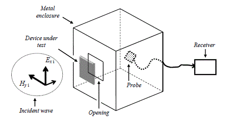
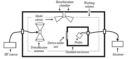
Figure 7.2shows the attenuation measurement carried out close to a transmitting antenna. We distinguish in (a) the configuration used for the reference measurement without the enclosure, and in (b), the measurement of the resulting field with the probe within the enclosure.
Figure 7.2. Measurement of the attenuation given by a shielded enclosure

This procedure will be called the insertion method. It thus requires the determination of a reference magnitude carried out under configuration (a), where we measure the power Pref, which is collected by the probe without the enclosure.Under configuration (b), the enclosure is inserted while keeping the distance dinvariant. The latter was initially set between the transmission antenna and the probe. Under these conditions, we measure the resulting power Pres seen by the probe. The attenuation provided by the enclosure can thus be expressed by a ratio formulated in dB:
[7.8] 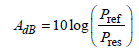
Under this configuration, the testing conditions have a more or less strong impact on the reproducibility of the measurements. The most impacting parameters will be the strong coupling with the transmitting antenna, as well as the location of the probe inside the enclosure. Let us assume that the frequency is tuned on the firsteigen mode of the box; it is then not surprising to find a negative attenuation. The latter means that the inner resulting field can have a higher amplitude than the reference field.
We will see in the next section that the use of reverberation chambers can partly erase the contribution of these testing configuration factors.
7.2.3. Shielding effectiveness of the materials
The definition related to the attenuation of a shielding material is currently established on the basis of the plane wave concept. The material is idealized by an infinite size plane of thickness e. A section of this plane is reproduced in Figure 7.3.
Figure 7.3. Configuration of an infinite plane material, illuminated by a plane wave

The figure has an oxyz coordinate system, whose oz axis carries the propagation direction of the waves. The ox axis carries the polarization of the electric fields, and the oy axis, the polarization of the magnetic fields. The “i” index is related to the incident wave, “ρ” to the reflected wave and “t” to the wave transmitted by the material. The arrows on the oz axis indicate the propagation directions. Therefore,the incident wave comes under the normal incidence angle.
The attenuation provided by the material will be characterized by the ratio of the amplitudes of the incident wave (incoming wave) and the transmitted wave. We will distinguish the attenuations produced on the electric and magnetic fields, i.e.:
[7.9] 
Figure 7.4. Configuration for the measurement of the relative attenuation of a material
The configuration described in Figure 7.3 can be achieved by standardized measurement methods, which are carried out on material samples with a finite dimension not exceeding a few centimeters. The device under test, thus constituted,is a barrier to the propagation of a wave, which is generated in a coaxial cell or in a TEM cell [WIL 88a, WIL 88b]. An extremely large range of frequencies going from a few kHz to several GHz is thus explored by these measurement methods. These techniques lead to the true attenuation of the material, which is also found in the standardized tests. In return, as soon as we need to know the impact of the attenuation for industrial application of the shield and assessment of its practical performances, then adopting the configuration shown in Figure 7.4. becomes more suitable. According to this method involving a shielding enclosure with a rectangular aperture, the sample under test is shunting the aperture. We typically find this situation during the use of composite materials, which are designed for the completion of the attenuation given by lightened metal structures.
The box irradiated by an electromagnetic wave, combines several physical phenomena. First, if we assume the aperture is undersized compared to the wavelength, the wave scatters throughout the aperture plane and in its immediate vicinity thus producing a near field emission within the enclosure. The field distribution in the enclosure depends on the ratio of the wavelength to the dimension of the box. Assuming that the physical properties of the shielding material sample which shunt the box, have little influence on the distribution of the inner field, we deduce the attenuation of the ratio of the powers received by the inside field probe –without and then with the sample on the box aperture. Formula [7.10] specifies the calculation of the attenuation, where Pref is the reference power without the sample,and Psp is the power collected with the sample shunting the aperture:
[7.10] 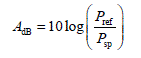
When the wavelength becomes similar or much lower than the dimensions of the aperture, this method gets closer to the definition of the attenuation. This definition is established under the hypothesis of infinite plane materials. The latter are illustrated in Figure 7.3.
We will see that the properties of the reverberation chambers enable us to reproduce the context of the attenuations, which are determined for ideally infinite planes or by the enclosure shunted by the shielding material sample.
7.3. Measurement of the effectiveness of shielded cables and connectors in reverberation chambers
7.3.1. Electromagnetic coupling on wires placed in a reverberation chamber
This section studies the electromagnetic coupling mechanisms occurring on wires illuminated by the ideal random field distribution of the reverberation chamber. We assume later in this section that the wires will be oversized with regard to the wavelength.
Although there are rigorous theories about these electromagnetic coupling phenomena, we will limit ourselves to an intuitive approach [HIL 93].
Let us consider a wire with dimension L0, which is positioned perpendicularly to a perfectly conducting plane with infinite dimensions. As shown in Figure 7.5, the wire is submitted to a plane wave, which is polarized so that the Ez electric field is parallel to the oz axis and the wire. The latter forms a monopole with the lower end connected on a resistance RL.
Figure 7.5. Description of the monopole and its equivalent circuit

The equivalent circuit on the right side of the figure will thus correspond to the monopole working as a receiving antenna. E0 represents the emf induced by the Ezfield, and Z0 is the inner impedance of the monopole. If we assume the wave is incoming under grazing incidence, the Ez projection is perpendicular to the ground plane and consequently Ez will be independent from the z variable. Under these conditions, we determine the induced emf with the help of integral [7.11], which is carried out on the only known distribution of current I(z), i.e.:
[7.11] 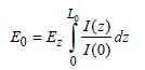
Assuming that I(z) follows the sine wave form [7.12]:
[7.12] ![]()
The calculation of the integral leads to the expression of E0:
[7.13] ![]()
If we ignore the frequencies where the current I(0) in the load RL vanishes, the emf goes through peak amplitudes for the specific wave numbers kq, according to the following equations:
[7.14] 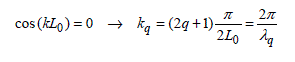
For all the fq frequencies, found from [7.14], we obtain the monopole’s resonances which produce the emf taking the specific amplitude (E0)q expressed below:
[7.15] 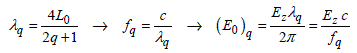
This behavior may be found again for any incidence angle of the plane wave. To ease understanding, we propose to use the reciprocity configuration corresponding to the monopole supplied by a RF generator. This amounts to replacing the RL load with a voltage source. Under this condition, the radiation is characterized by a radiation pattern with different radiation lobes, which become more numerous as the ratio of the monopole size to the wavelength increases. Thus, when the frequency of the sine wave source is exactly tuned to the first resonance planned by relationship [7.14] (when q = 0), we find a single radiation lobe, whose maximum amplitude direction is perpendicular to the monopole. This means that for the monopole used as a receiving antenna, a wave incoming under any incidence does not modify the value of the resonance frequency, but its direction of incidence yield lowers the amplitude of the induced emf, which is calculated in [7.15].
Increasing the frequency of the RF generator in order that the monopole becomes oversized with regard to the wavelength, it implies resonances corresponding to qindices higher than 1. Then we observe that the number of radiation lobes is proportional to q. Consequently, any incoming plane wave with an incidence angle θwith respect to the axis of the receiving monopole produces an emf established by relationship [7.16]. This relation introduces the function D(θ), the directivity of the monopole defined in section 3.5.1 of Chapter 3 or section 6.2.3 of Chapter 6.
[7.16] 
In order to link the amplitude of the plane wave with the power balance in the monopole, let us seek a physical interpretation of the inner impedance Z0, which has been mentioned in the equivalent circuit in Figure 7.5.As previously, let us pay particular attention to the behavior of a resonant monopole. Using the reciprocity principle of antennas, we know that, for the resonances defined according to equation [7.14], Z0 is the radiation resistance of the monopole, which is presently designated by the (Rr)q notation. Let us recall that the radiation resistance is deduced from the calculation of the flux of the Poynting vector, which is carried out for the far field and throughout an hemispherical surface centered on the bottom of the monopole:
[7.17] ![]()
The matching condition of the monopole operating under the qth resonance thus consists of choosing a load resistance RL, which is rigorously similar to (Rr)q, i.e.:
[7.18] ![]()
Under these conditions and for any incidence angle of the incoming plane wave,the power losses in the load takes the expression:
[7.19] 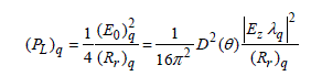
If we extend the previous conditions for a monopole exposed to an ideal random field distribution, the power collected (PL)q on the load behaves as a random variable. The moment of (PL)q can be expressed according to relationship [3.131](section 3.5.2 of Chapter 3). We recall that equation [3.131] and consecutively formula [7.20] are established on the model of the randomly distributed plane waves as mentioned in Chapter 3.
[7.20] 
We find again in this formula the wave impedance Zw of 377 Ω, as well as the amplitude Ew of the plane waves achieving the random field distribution.
Later we will return to the link between expressions [7.19] and [7.20]. But first,let us take a look at the effective area of a cable or a shielded connector.
7.3.2. The effective area of a cable or a shielded connector
Let us imagine the monopole in Figure 7.5 made up of a coaxial cable matched at both ends, with the top termination connected on a resistance and the bottom end on the input port of a receiver such as a spectrum analyzer. Figure 7.6. gives us more detail about the configuration of the cable and its load terminations. Assuming that this cable is exposed to an ideal random field distribution, let us designate with thePL’ notation, the power collected on the receiver at bottom of the cable termination.Under these conditions, the average power collected on the qth resonance according to relationship [7.15], will be expressed with the help of the notation conventions below:
[7.21] 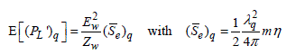
Figure 7.6. Combination of a monopole and a shielded cable in view of the concept of effective area
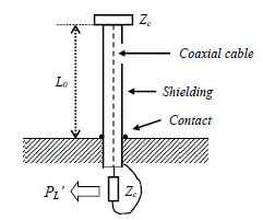
This new expression includes the average effective area determined by use of the formula where appear the mismatch coefficient m and the antenna efficiency η of the device. Since the outer side of the shield is similar to the monopole in Figure 7.5, whose bottom is now short-circuited, and assuming the shield provides high attenuation, active energy will be mainly transformed into the thermal form due to losses along this tubular shield.
Consequently, the antenna efficiency η that appears in equation [7.21] will be much lower than 1. This low antenna efficiency contributes to decrease dramatically the average effective area, which is much lower than the value found in [7.20] for the non-shielded monopole. We need to specify that the mismatch coefficient is mainly related to the impact of the distribution of the induced current on the outer surface of the tubular shield. Additional comments about the behavior of the effective areas of transmitting antennas and receiving antennas in a reverberation chamber may be found in [JUN 11].
From the previous considerations, we manage to determine the attenuation AdBof the tubular shield by forming the ratio of the power losses E[(PL)q] in the resistance RL of the matched monopole and the power collected E[(PL’)q] at the end of the shielded cable, i.e:
[7.22] 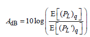
This attenuation is therefore strictly similar to the ratio of the effective area of the matched monopole and the effective area of the shielded cable:
[7.23] 
This relation, here restricted for the resonance frequencies of the monopole, can be extended to any frequency by setting out:
[7.24] 
The main interest brought in these formulas comes from the direct link with the simulation of the coupling phenomena by the plane wave interference, as seen in section 3.3 of Chapter 3. The following demonstration consists of specifying the configuration of the devices under test, in the context of a measurement or of a calculation. Then, we will establish the link between the concepts of effective area and transfer impedance.
7.3.2.1. Configuration of the devices under test, in the context of a calculation or a measurement
The set up for measurement or computation of the shielding effectiveness of a shielded cable or connector in a reverberation chamber must be arranged according to the following conditions. If the test concerns a shielded cable, the length ΔL of the sample of the cable exposed to the random field distribution has to remain – as much as possible – far lower than the wavelength. This condition is required in order to reduce the effects of the propagation phenomena on the inner conducting wire.
Conversely, the L0 dimension of the shielded junctions placed at both sides of the cable under test will be as far as possible oversized with regard to the wavelength.The diagram on the left side in Figure 7.7. specifies this specific configuration, as well as relationship [7.25] below:
[7.25] ![]()
In the case of a test involving a shielded connector, a similar configuration will be adopted as recalled in the diagram on the right side. In Figure 7.7 the HI abbreviation means that we require high immunity shielded cable with very low transfer impedance for the shielded junction at both ends of the sample under test.
Figure 7.7. Configurations of the devices under test for a calculation or a measurement

Indeed, the use of the shielded junctions is useful to insert the short sample of length ΔL of the cable under test in the middle an oversized wire. Furthermore, the sample of length ΔL must lie within the working volume of the room according to section 4.2.4 of Chapter 4.
On the other hand and in order to conform with the description in Figure 7.6., the HI shielded junctions must be matched at both end on their own characteristic impedance Zc.
7.3.2.2. Calculation of the effective area of the shielded cable
If the device under test remains small compared to the wavelength, the input of the transfer impedance defined in section 7.2.1, leads to the following expressions of the collected power:
[7.26] 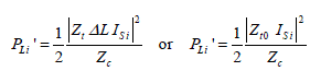
In these two relationships, we find again the transfer impedance Zt of the device under test, if it is a shielded cable, and Zt0 in the case of a shielded connector. The iindex refers to a plane wave of any incidence, polarization and phase angle. This wave illuminates the devices described in Figure 7.7. The ith plane wave induces the current ISi found in expressions [7.26], on the outer part of the length ΔL of the shielded sample. The use of these relations assumes that the resulting power coupled through the HI shielded junctions remains clearly negligible.
According to the features of the plane wave spectrum as detailed in section 3.5 of Chapter 3, the power collected on the device under test may be expressed by equation [7.27] where the Sei effective area is attached to the ith plane wave of amplitude Ew.
[7.27] 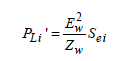
Knowing that the amplitude Ew of the wave is kept invariant, the calculation of the moment of the PLi’ random variable leads to the determination of the average effective area of the device under test, i.e.:
[7.28] 
Under the conditions of a numerical simulation, the computation of ![]() is made up of a sample of N plane waves, leading to the estimate of the mean value < Se >:
is made up of a sample of N plane waves, leading to the estimate of the mean value < Se >:
[7.29] 
If we transpose the previous equation for the measurement carried out in a reverberation chamber, the sample size will be given by the NS angular positions of the stirrer providing independent random data.
The estimated effective area can then be introduced into equation [7.24], which is used for the definition of the attenuation of the devices under test thus laid out.
7.3.3. Relationship between the reference power and the current induced on a device under test
Let us come back to the behavior of the monopole loaded by the resistance RLand under the configuration presented in Figure 7.5. We obtain the balance of two phenomena on any resonance frequency of the monopole and for a matched load resistance. The measured power due to the thermal losses in RL is almost similar to the power radiated by the monopole due to the induced current by the incoming wave. This power is then converted into a thermal form in the walls of the room and other devices in the chamber. A tiny part of this power will also be lost in the wire forming the monopole. In other words, the contribution of the radiation due to the current induced on the monopole only impacts the distribution of the standing wave sand has a negligible effect on the damping of the chamber.
According to the previous description of the phenomena, when the bottom end of the monopole is directly connected to the ground plane (RL =0) the thermal losses involved in the coupling of the waves will be almost negligible throughout the monopole. There remains almost only the radiated power from the monopole and therefore also the disturbance produced on the field distribution in the chamber.Thus, these conditions are very close to the configurations found in Figures 7.6 and Figures 7.7, where the resulting power PLi’ collected over the length ΔL of the sample was related by equation [7.26]. The determination of the rigorous mean value of PLi’then requires the computation of the moment of the square ISi current, hence:
[7.30] 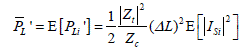
Generally, direct measurement of the ISi current is not easy. Moreover, this measurement can be seriously disturbed by the coupling with the current probe.Thus, is more suitable to deduce ISi from the power collected by a receiving antenna.
Indeed, expression [7.28] means that any receiving antenna with an average effective area ![]() collects an average power that is the moment of the random
variable Pcr that represents the collected power data.
collects an average power that is the moment of the random
variable Pcr that represents the collected power data.
[7.31] 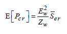
We find at the numerator of this formula the amplitude Ew of the plane wave spectrum as used in equation [7.28] above. This is an interesting formula, because the product of the square of Ew with the effective area of the antenna leads to the introduction of the new V0 variable which represents a voltage:
[7.32] ![]()
According to this analogy, we reach a relation in which the average collected power is similar to the fictitious power losses in the plane wave impedance Zw(377 Ω) fed by a voltage source V0.
[7.33] 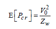
According to the Norton theorem, this relation can be transformed following form [7.34] below, where the average power is similar to the power losses in the impedance Zw fed by a current I0 which is the ratio of V0 over ZW.
[7.34] 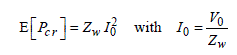
It thus remains to try to establish a link between I0 and the current ISi induced on the external surface of the ΔL length of the shielded cable under test.
We assume that the dimension L0 of the cable arrangement is oversized with regard to the wavelength, and that the sample of length ΔL is placed in the middle of this set up. We can then conclude that the statistical behavior of the ISi data,especially the moment of the square of ISi remains independent of the location of the sample of shielded cable in the chamber. Consequently, the moment of the square ofISi is similar to the square of I0 found in equation [7.34].
[7.35] ![]()
We find immediately the link between the power collected on the reference antenna and ISi:
[7.36] 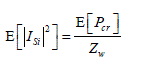
This computation was based on the assumption of ideal matched condition of the receiving reference antenna. However, it is obvious that the random features of thePcr and ISii data leads to the extension of relationship [7.36] to any other frequency,as long as the oversizing condition is met.
7.3.4. Conversion of the shielding attenuation into a transfer impedance
Generally and above 1 GHz, the measurement of the shielding effectiveness of cables or shielded connectors consists of the determination of the transfer impedance characteristic [DEM 11a]. Several measurement methods have been the subject of international standards, notably those published by the International Electro technical Commission. As soon as the frequency overlaps a few GHz, these measurement techniques become unsuitable since enforcing the hypotheses of the TEM wave approximation, which is assumed according to the definition of the transfer impedance found in section section 7.2.1. Conversely, determination of the shielding attenuation in reverberation chambers is well suited for frequency range higher than1 GHz. In order to normalize the results on a very wide frequency band, conversion rules must be established, in order to go from the shielding attenuation to the transfer impedance or inversely
The approach used is then based on the link between the current ISi induced on the cable shield under test and the power Pcr collected on a receiving antenna as detailed in the previous section. We will carry out the conversion of the AdBparameter towards Zt. We will not have any difficulty in versing the obtained relation. Measurement of the power collected on the device described in Figure 7.7.will thus require the estimate of the PL’ data. The shielding attenuation will thus result from the ratio of the estimate of the mean value of the Pcr power data collected on the reference antenna over the estimate < PL’ >, either on linear scaleAlin or dB scale, AdB:
[7.37] 
After use of the estimate notations, equation [7.30] established above and its similar form for a test carried out on a shielded connector, will be expressed in two distinct formulae.
[7.38] 
Furthermore, from equation [7.36], we find that the estimate of the moment of the square of ISi, i.e. the current induced on the cable shield under test, is easily deduced from the estimate of the mean value of the power Pcr collected on the receiving antenna.
Hence:
[7.39] 
After substitution of [7.39] into [7.38], we can link easily the transfer impedanceZt with the shielding attenuation Alin with equations [7.40]. In these equations the notation ^ stands for estimate:
[7.40] 
These formulae may be also presented with the attenuation in dB scale. They take form [7.41], so that we find them in the IEC standards:
[7.41] 
Let us specify that the estimate of the transfer impedance is subjected to the uncertainty dependent on the size of the samples of independent data, which are assumed to be collected during a rotation of the mode stirrer.
7.3.5. Examples of the measurements of the shielding effectiveness of the connectors
7.3.5.1. Description of the device under test
The measurements shown in this section are carried out with a short sample of coaxial cable section with a shield composed of a copper pipe of 0.1 mm thickness and 12 mm diameter. The electromagnetic leakage, whose transfer impedance we seek to determine, is provided by a small circular aperture of 10 mm diameter. Figure 7.8 specifies the geometrical description of this device that we can compare to the electromagnetic coupling occurring throughout a usual shielded connector.
The main advantage of this configuration is that it produces a transfer impedance, which evolves with a law proportional to the frequency.
Figure 7.8. Description of the device used for the transfer impedance measurement

7.3.5.2. Physical properties of the device under test
The electromagnetic coupling theories carried out on tubular shielding with small apertures show that the transfer impedance is in that case made up of the sum of two terms gathered under the following notation [BOU 09, DEM 81, LEE 75,VAN 75]:
[7.42] ![]()
In this formula, the term Ztd deals with the propagation throughout the copper pipe thickness of the complex electric field projection which is parallel to the pipe axis. The term Lt plays the part of an inductance of mutual coupling, involved in the leakage of the magnetic azimuthal field projection, coming from the current flowing on the shield. This so-called transfer inductance Lt comes from the scattering of the magnetic field through a set of similar small apertures. We can attach to Lt an analytical formula, involving successively the outside diameter of the shield Dassumed to be lower than the wavelength, the density of apertures ν and the coefficient αmθ called the “magnetic azimuthal polarizability of the aperture”:
[7.43] 
μ0, the constant of absolute magnetic permeability, also appears in this formula. Experience proves that for frequencies exceeding several MHz, the contribution of the transfer reactance Ltω becomes predominant compared to the Ztd term.
Moreover, if the device under test only has one aperture (ν = 1), the leakage is localized and the transfer impedance found in the left part of [7.42] appropriates theZt0 notation previously adopted for the shielded connectors, i.e.:
[7.44] ![]()
In the case of a circular aperture of diameter d, computation of the αmθcoefficient can be performed by the analytical way according to the following expression:
[7.45] 
However, use of this formula, taken from the theory of field diffraction(scattering by small apertures) assumes that the diameter d of the aperture remains much lower than the wavelength and that the shield thickness remains negligible compared to d.
For the geometrical data found in Figure 7.8, calculations lead to a transfer inductance of 0.72 nH. Transfer impedance measurements carried out on a tri-axial bench whose principle is presented in [DEM 10, DEM 11a] combined with the transfer impedance deduced from shielding attenuation measurements in reverberation chambers will be compared with the theoretical values of Zt predicted by equation [7.42].
7.3.5.3. Comparison of the theoretical laws and measurements
Figure 7.9. gathers three curves of transfer impedance covering the range of frequencies from 100 MHz to 10 GHz presented in a logarithmic scale [BOU 09].
The dotted line is the theoretical curve which is rigorously proportional to the frequency. The shorter thick line over the 100 MHz to 1 GHz frequency range gives the transfer impedance directly measured on a tri-axial bench. The bench was configured according to the method of shielding discontinuity, which is described in the thesis by L. Koné [KON 89] and in [DEM 11a]. The continuous line corresponds to the values of Zt0, which are deduced from the shielding attenuation given in a reverberation chamber according to the procedure presented above and more detailed in the following sections.
Figure 7.9. Transfer impedance characteristics of the device with a small aperture

The device under test is placed in the chamber in the recommended configuration depicted in Figure 7.7.
The tests have been carried out in a reverberation chamber with a volume of72 m3 with a minimum presumed frequency fs of 200 MHz. The data thus recorded covers the 200 MHz to 10 GHz frequency range.
We will notice a good agreement of the direct measurements of Zt on the tri-axial bench with the predicted values found from equation [7.42]. The transfer impedance values deduced from the attenuation measurements in reverberation room are also similar to the previous values. However, a carefully look at the curves reveals a few differences with the theoretical result which exhibits a dotted straight line.
At the beginning of the range and more especially between 200 MHz and500 MHz, the curve taken from the test in reverberation chambers shows some amplitude fluctuations. These fluctuations may be caused by the contribution of a few phenomena. Indeed, in the neighborhood of 200 MHz, the length of the HI shielded cables linking the device under test to the loads is not necessary oversized with regard to the wavelength. This condition was required by the procedure described in section 7.3.4. Moreover, this frequency range is located close to the condition where the field in the room does not yet follow an ideal random distribution as expected in the reverberation chamber theory. Such conditions involve systematic errors caused by the non stationary stochastic behavior of fields in the room. This produces a lower level of reproducibility of the measurements.However, above 500 MHz, such fluctuations tend to disappear. This confirms that we reach progressively the stationary stochastic behavior of the room. On this matter, we need to specify that in order to reduce the random fluctuations obtained with the mode stirring caused by the non stationary behavior mentioned above we process to a moving average, on ten consecutive frequency samples, as presented in the discussion concluding this chapter.
After 3 GHz, the transfer impedance estimation deduced from the shielding attenuation significantly moves away from the theoretical values. However, so far,we have not shed light on the cause of this behavior. We should probably add other electromagnetic coupling to the leakage involved by the azimuthal projection of the magnetic field, the only coupling mechanism considered in relationship [7.44]. Studies written about this matter by F. Broydé [BRO 93] point out the participation of five coupling modes. Some of them can have an influence at frequencies over1 GHz. The definition of the transfer impedance for a device exposed to the field established in reverberation chamber may be also questionable [DEM 11b].
7.4. Measurement of the attenuation of the shielded enclosures
7.4.1. Expected electromagnetic coupling mechanisms
The measurement procedure of the attenuation of a shielded enclosure in reverberation chambers as described in this section comes from the method briefly described in Figure 7.2. In order to fulfill the conditions of reproducibility of the measurements and therefore to keep the stationary stochastic features of the field distribution in the room, the enclosure under test must be placed within the working volume defined in section 4.2.4
Collecting the reference power Pref found at the numerator of equation [7.8] can be carried out in two different ways, depending on whether it is recorded with or without the device under test
We can notice that the field calibration carried out with the device standing in the room gives the advantage of accounting for the thermal losses in the enclosure,and consecutively of leading to the actual reference magnitude Pref. The measurement of the resulting power Pres is carried out with the probe placed in the device. To determine the best location of the probe within the enclosure, a preliminary analysis of its inner configuration is necessary.
Unlike the reverberation chamber, the device under test is not necessarily oversized, compared to the wavelength. This means that the resulting field distribution found inside a good shielded enclosure will be mainly due to the various leakages through the wall surface of the box. This can thus lead to a quality factor sufficient for the excitation of the first eigenmode of this enclosure behaving like a second cavity coupled to the reverberation chamber. Under these conditions and as a function of the location of the probe inside the enclosure, the amplitude of the resulting power Pres can vary in quite large proportions. The resonance of the apertures can be added to these first phenomena, whose contribution can become significant as soon as there are slots in enclosure walls.
Consequently, measuring the attenuation given by a shielded enclosure requires the careful examination of the previously expected phenomena. When there are relative measurements, the technological choice of the probe does not have the same rigor as in the electromagnetic immunity tests. Quite suitable results will be obtained with the help of probes made up of a printed trace set on an insulating substrate leant against a conducting ground plane. Let us specify that the collection of the data batches recorded on a few locations of the probe in the enclosure can reduce the uncertainty, by carrying out a mean estimate.
However, when the volume occupied by the enclosure is sufficient to behave like an oversized cavity, the room and the enclosure behave as two coupled reverberation chambers, Mechanical mode stirring and frequency agitation may be combined in the two oversized cavities according to the methods described in section 4.3.1 and section 4.3.2. This will lead to a significant reduction of the uncertainty margins for the determination of the AdB parameter.
7.4.2. Example of attenuations measured on a shielded enclosure
The example is about a rectangular slotted cavity. The field probe will be made of a small electric monopole, 1.8 cm in dimension and normally fixed at the inner sides of the walls. Figure 7.10. specifies the geometrical data of the cavities, as well as the location of the probe.
To display the curves, the definition of the attenuation prescribed by [7.8] has been in versed to conform to the expression below, where we can find at the numerator the resulting power Pres collected on the probe within the cavity. On the other hand, we can find at the denominator the reference power Pref, i.e.:
[7.46] 
A negative value means that the enclosure brings an attenuation. On the contrary,a positive value indicates a possible strengthening of the field amplitude measured at the probe’s location inside the enclosure.
Figure 7.10. Example adopted for the attenuation measurement of the shielded enclosure

Conforming to the right side of the figure, the reference power Pref comes from the monopole placed above a ground plane and exposed to the field of standing waves of the reverberation chamber. The rectangular slot on the upper side of the cavity has a width of a few millimeters and a dimension L0 of 10 cm. Figure 7.11 has two curves showing the variations of AdB’ versus the frequencies located between 500 MHz and 10 GHz.
The measurements were carried out in a reverberation chamber, whose lowest usable frequency fs is located at 500 MHz. The thick line gives the estimate of AdB’,when we form the ratio of the estimated average of Pres and Pref parameters found in equation [7.46]:
[7.47] 
Each average is performed on a set of 50 pieces of data coming from 50uniformly distributed angular positions of the mode stirrer. The thin line corresponds to the same measurement procedure carried out after insertion of a lossy material in the cavity under test.
These results suggest a physical interpretation that we will summarize through a division of the explored frequency spectrum in three areas. Each of them is linked to a very specific behavior. From 500 MHz to 1 GHz, the additional thick straight line shows a slope close to 15 dB by octave. This corresponds to an attenuation fall of 22dB by decade. Consequently this suggests that the coupling produced by the slot increases the receiving power at the monopole load by a factor close to 160 when the frequency grows from 100 MHz to 1 GHz. This represents about a 12 fold increase of the voltage induced on this presently electrically short monopole.
Figure 7.11. Recorded measurements of the attenuation given by a shielded enclosure with a slot
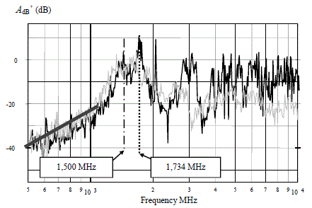
Indeed, between 100 MHz and 1 GHz, the dimension L0 of the slot fixed here at10 cm, remains small with regard to the wavelength and, the coupling of the field throughout the slot is similar to the radiation of a Hertzian dipole at a near field distance from the slot. As recalled in Appendix 5, the amplitude of the near electric field projections remains invariant with the frequency. Due to the capacitive nature of the monopole impedance, the resulting voltage collected on the 50 Ω input resistance of the receiver is therefore proportional to the frequency.
Above the frequency of 1 GHz, the shape of the curves change dramatically, and we observe as well a series of fluctuations of the attenuation, which can be allocated to various resonance phenomena. Three resonance mechanisms will be combined,one comes from the shielded box itself, the two others are derived from the slot and the monopole. Regarding the resonances of the shielded box, Table 7.1 gathers the first 14 eigenmode frequencies, which are calculated according to relationship [2.56] devoted to the empty rectangular shaped cavity.
These natural resonances of the cavity are combined with the first mode of resonance of the slot, currently located at 1,500 MHz, and the first resonance of the 1.8 cm monopole, which is located at the frequency of 4,160 MHz.
We can notice the resonance of the slot located on the graph by the vertical dash and point dotted line, while the third eigenmode of the cavity presently located at 1,734 MHz, is indicated by the vertical point-dotted line. We observe that the value of the AdB’ attenuation collected at 1,734 MHz is positive and reaches its peak at+ 10 dB. Consequently, we can say that the power collected by the monopole inside the slotted metal box is for this peculiar frequency higher than the reference power induced on the monopole according to the configuration on the right side in Figure 7.10. This much localized behavior shows – quite well – the impact of the quality factor of the shielded enclosure, whose third eigenmode is very strongly excited.
Looking at the 1,500 MHz slot resonance, this latter seems more damped than the previous one. This is probably caused by a higher back scattering of the energy towards the outside of the cavity. Between 2 and 4 GHz, other fluctuations occur.They are more or less correlated to the eigenmodes of the cavity. Analysis of the phenomena is however difficult insofar as the power collected by the monopole is dependent on its relative location towards the field distribution in the box.
Table 7.1. Location of the 14 first eigenmodes frequencies of the empty cavity illustrated in Figure 7.9

Above 4 GHz, the natural resonances of the monopole are combined with the resonances of the cavity, whose functioning evolves towards an oversized behavior compared to the wavelength. The room and the box then behave like two oversized coupled cavities.
A means of reducing the fluctuations of amplitude would consist of producing a mode stirring inside the device or of combining the frequency agitation with the rotation of the mode stirrer installed in the chamber. In order to increase the losses in the shielded box, we have inserted in it a piece of electromagnetic absorbing material. The thin line in Figure 7.11. corresponds to the shielding attenuation collected for this configuration. With respect to the previous experiment, where no absorbing material was present, we observe a reduction of fluctuation amplitude sand consequently, of the resonance amplitudes of the shielded box. We intuitively know that the contribution of these additional losses in the box is practically without any influence on the resonance of the slot located at 1,500 MHz and on the fluctuations which are observed below this frequency. The natural uncertainty margin of the reverberation chamber, fixed during the field calibration, explains these fluctuations for this low frequency band.
7.5. Measurement of the shielding effectiveness of the materials
7.5.1. On the size of the devices under test with respect to the wavelength
7.5.1.1. Method of the coupled rooms
Figure 7.12. represents the longitudinal cutout of a reverberation chamber, which is configured in order to carry out an attenuation measurement of materials following the principle of the coupled rooms. The device under test is made up of a plane placed in the median (middle) part of the chamber with the help of uniform and good contacts carried out with the metal walls. The inner volume of the chamber is thus divided into two coupled rooms with the device under test as a common wall.One room, located on the left side, corresponds to the area of transmission of electromagnetic waves. The other room, on the right side, collects the resulting waves which have traveled throughout the barrier made up of the sample of material.
Figure 7.12. Test of a material according to the method of coupled rooms

The sample of material under test thus occupies the full cross-section of the chamber. We may therefore make use of the electrical image theory resulting in a infinite expansion of the images of this sample on both sides of the parallel walls to the sample plane. For these reasons, the device under test is similar to a plane with infinitely virtual dimensions. The emission carried out in the left area of the chamber and above the lowest frequency fs, makes sure that the screen will be imperatively oversized compared to the wavelength. The mode stirring involving random field distribution, all happens as if the sample was illuminated by a large number of incoming plane waves with randomly distributed polarizations and incidence angles.These waves interact with the material in order to produce in the right area of the chamber attenuated standing waves, whose amplitude is measured by the probe connected to the receiver. When the material offers sufficient attenuation, i.e. at least higher than 20 dB, the sample behaves as a hard barrier for electromagnetic waves.This means that the distribution of the waves in the right area is almost not correlated with the random field found in the left area. Under these conditions, it seems suitable to combine into the right area of the room another mode stirrer, so that the probe collects purely stochastic data.
After the use of equation [7.10] where the attenuation is expressed by the ratio of a reference power and of the power collected in the shadow side of the sample, we must seek a reference power which is influenced as little as possible by the coupling of the waves on the sample. A possible method would consist of measuring the power received on the probe without the sample. The main drawback of this solution comes from a bias error, caused by the strong changes of the field properties, in the emission area, after insertion of the sample. For these reasons, it seems more suitable to carry out the reference measurement with the sample, by making the probe swerve in the emission area, in order to estimate < Pref >, and then to carry out the estimate of the resulting power < Pres > in the shadowed area. The measured attenuation is then expressed:
[7.48] 
Although this measurement procedure is close enough to the assumption of the illumination of an infinite plane sample, the attenuation collected according to equation [7.48] moves away from the theoretical definition given in [7.9]. Indeed,equation [7.9] is defined as the ratio of the amplitude of the incident wave on the transmitted wave. As proven by the simple reasoning discussed below, in the context of the test in a reverberation chamber, the amplitude of the incident wave isunknown.
To simplify, we can assume an infinite plane sample, which is located in free space. In the frame of the coupled rooms method, the attenuation given in the previous equation [7.48] is then formulated below:
[7.49] 
At the numerators we find the algebraic sum of the incoming incident wave and the wave reflected back from the sample. Assuming the free space condition in the shadow area of the sample, we find only the transmitted forward wave at the denominators of [7.49]. The analogy means that in the transmitting area, the observer detects a standing wave recalling the configuration reproduced by the test carried out in reverberation chambers. Thus, the measurement in reverberation chambers according to this method moves away from the definition used in relationship [7.9].
Although frequently used in acoustics, the protocol of the coupled room is seldom adopted for electromagnetic wave irradiation because of the important size required for the sample of material under test and the various leakages at the contact areas between the sample and its supporting structure in the chamber.
7.5.1.2. Method of the shunted shielded enclosure
This method uses a shielded enclosure whose aperture receives the sample material as more precisely described in Figure 7.4. The device thus constituted is installed in the working volume of a reverberation chamber, which is materialized in the cutout of Figure 7.13 by the outline in dotted line. To meet this geometrical requirement, we can install the shielded enclosure on a non-dissipative insulating support [COD 07].
The shielded enclosure and a fortiori the device under test are not necessarily oversized compared to the wavelength. Thus, it can lead to an impact on the estimate of the attenuation measurements.
As briefly specified by the protocol in section 7.2.2, we carry out measurement sin two different configurations according to a substitution method. We measure beforehand the reference power Pref received on the probe without the device under test, and then we measure the resulting power Pres when the material under test shunts the aperture located on one of the sides of the shielded enclosure. As it is a relative measurement, we will pay attention during these two stages not to modify the location or the polarization of the probe inside the enclosure. The latter is not necessarily oversized and therefore, nothing proves that the field in the enclosure respects the ideal random distribution required by the subsequent stochastic processing.
Figure 7.13. Location of the shielded enclosure inside a reverberation room in view of the measurement of the attenuation of a material sample
Indeed, we deduce the attenuation of the ratio of the estimates of the Pref and Presmean powers, which are calculated after a rotation of the mode stirrer:
[7.50] 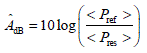
Let us specify that expression [7.50] can be easily converted under voltage measurements which are supplied by the probe, by passing through the Vref and Vresnotations, i.e.:
[7.51] 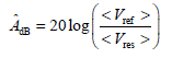
According to this procedure, we admit that during a measurement carried outwith a probe at a fixed location, the attenuation deduced from expressions [7.50] or[7.51] will be related to the barrier against electromagnetic waves introduced by the sample of material under test. Nevertheless, for the physical reasons mentioned in section 7.2.3, the attenuation found by this protocol can be very different from the theoretical attenuation of infinite plane materials, which are illuminated by a single plane wave and under the normal incidence.
7.5.2. Examples of attenuation measurements carried out on a material
7.5.2.1. Brief description of the material
The test concerns a conductive polymer carried out by the Ecole Superieure des Mines de Douai (a French engineering school). This material has as a basic component: the doped polyanimine mixed with a solvent [HOA 07]. It can be found in the form of a film or a liquid solution coated on an insulating substratum. The devices under test carried out for the implementation of the attenuation tests will use the solution coated on a glass fiber plate forming a plane square surface with 15 cm sides. This thin layer of conducting matter of a few hundredths of a millimeter thickness can reach an electric conductivity higher than 10,000 S/m according to the doping rate.
7.5.2.2. Practical configuration of the sample under test
In order to carry out the attenuation measurement in reverberation chambers, we shunt the aperture of the shielded enclosure with the sample as, shown in Figures 7.4 and 7.13. The box will be made up of a rectangle of 28 x 38 x 41 cm dimensions.The upper side carrying the largest dimensions will form the lid with the aperture receiving the sample [KON 06].
Figure 7.14. Longitudinal cutout of the receiving line and of the sample under test

The energy coupled in the enclosure is collected by a transmission line placed in the middle of the box. One termination of this line is loaded by a resistance of 50 Ω,while the opposite end is connected on the receiver. Figure 7.14 gives a longitudinal cutout of the box arrangement, on which we recognize in the upper part the installation of the device under test. The side of the substrate coated with the conductive polymer gets into contact with the metal lid of the enclosure with the help of screws in order to insure a good electrical contact on the sample flange.
The measurements were first carried out in a TEM cell, in order to cover the range of frequencies 100 kHz – 100 MHz. As recalled in section 1.3.2 of Chapter 1, the highest frequency is governed by the cross-section dimensions of the cell. The enclosure is then fixed on the ground plane with the device under test directed towards the septum.
In a first test aimed at vanishing the contribution of the magnetic coupling, the box is rotated in order to maintain the inner receiving line perpendicular to the axis of the TEM cell. Under these conditions, the voltage collected on the inner line is thus only due to the coupling induced by the electric field projection, which is perpendicular to the ground plane of the cell. In a second test, both electric and magnetic couplings will be involved. For this, we rotate the box by 90°, in order to make the receiving line parallel with the axis of the cell. Knowing that in this test the electric coupling brings a weak contribution compared to the magnetic coupling,the second test gives direct access to the magnetic phenomenon.
To ease the display of the results, the attenuation measured in the TEM cell will be determined by the AdB’ ratio of the powers captured on the receiver, where Pres is measured with the device under test and Pref without:
[7.52] 
Figure 7.15 gathers the results of the shielding effectiveness found in the TEM cell for couplings carried out independently by the electric field (dots), and then by the magnetic field (solid line). We observe that the attenuation for the electric field is extremely strong. In fact, the dots on the graph correspond to the noise floor of the receiver connected to the receiving line, which is located within the shielded enclosure. This result means that the Pres term at the numerator of equation [7.52] is invariant, whereas the reference power Pref collected on the line without the sample behaves with a law proportional to the frequency of the RF generator, which is connected to the input of the cell.
Indeed, within the considered frequency range (100 kHz – 100 MHz) and with the size of the enclosure remaining much lower than the wavelength, the reference power Pref almost obeys to quasi-static electrical phenomena. Under these conditions, the electric field induces on the receiving line a current proportional to the frequency.
Figure 7.15. Results of the sample attenuation as measured in the TEM cell

Conversely, as long as the frequency remains lower than 10 MHz, we realize that the device under test is almost transparent to the magnetic field. This behavior is easily explained by considering that the surface resistance of the sample under test is too high to divert the current induced on the highly conducting surface of the enclosure. However, as soon as the frequency overcomes tens of MHz, the amplitude of the tangential electric field which is generated in the aperture plane containing the sample under test, becomes sufficient to stimulate induced currents generating an additional magnetic field which is opposite to the incoming field.
This phenomenon appears more clearly in Figure 7.16, devoted to the results of the experiment carried out in a reverberation chamber. On the top of the graph, we observe the shielding effectiveness deduced from the data collected for the test of the conductive polymer material. The range of the explored frequencies goes from the lowest usable frequency of the chamber located close to 500 MHz to the maximum frequency supplied by the RF generator, i.e. 10 GHz. The second curve ofAdB’ under the previous one is obtained when the aperture is shunted by a copper screen 0.5 mm thick. The very significant attenuation caused by this highly conducting screen enables us to locate the sensitivity threshold level of these measurements, whose minimum is close to -80 dB.
We will note that in the best conditions, this threshold level is located 40 dB below the attenuation given by the conducting polymer sample. We must specify that the decreasing shape of the curve observed below 700 MHz is to be linked to the noise floor of the receiver. The behavior is in this place quite similar to the threshold detected during the coupling measurement under electric field coupling in the TEM cell. Above 1 GHz, the rise of AdB’ is due to the increasing electromagnetic leakages, which are mainly produced on the edges of the shuntedaperture.
Figure 7.16. Curves of shield attenuation measured in the reverberation chamber
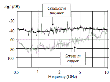
It is not surprising to see this curve meet the previous one at about 10 GHz. This means that at these very high frequencies, the leakages occurring on the edges of the sample overcome the coupling of the waves throughout the conductive polymersample.
The random fluctuations are quite visible on these curves. They are to be linked to the uncertainties on the estimates of the mean values of Pres and Pref, found in the determination of AdB’ mentioned below:
[7.53] 
To improve the readability of the results, curves in thick solid lines added to the previous one are built up from a moving average on a set of ten successive data.
Figure 7.17 gathers, on the same graph, the measurements carried out on the conducting polymer sample, for tests carried out successively in TEM cells, in anechoic chambers and in reverberation chambers.
Between 1 MHz and 100 MHz, we find the curve recorded in Figure 7.15, when the device is exposed to the magnetic coupling produced in the TEM cell.
From 100 MHz to 1 GHz, the AdB’ coefficient is the result of a measurement which is carried out in an anechoic chamber, according to the substitution method described in section 7.2.2. The reference power Pref is determined with the shielded enclosure according to the configuration found in Figure 7.13, without the sample under test. The resulting power Pres then corresponds to the power received with the sample. We can notice that to produce the conditions of a magnetic coupling, the transmitting bi conic antenna was vertically polarized in front of the aperture receiving the device under test. The incoming wave is under normal incidence.
Figure 7.17. Behavior of the shielding effectiveness of the conducting polymer on a very large frequency range

The results recorded from the measurements carried out in rever beration chambers are within 500 MHz to 10 GHz (upper curve of the graph of Figure 7.16).
We will notice the good agreement between overlapping curves, whose maximum amplitude range is close to 50 dB.
The peak, indicated by the fr marker, corresponds with a resonance of the shielded enclosure carrying the sample under test. It is related to one of the first eigenmodes of this rectangular cavity.
We will note that below this resonance, the fluctuations observed on the obtained results in reverberation chambers are of smaller amplitude than above fr. This behavior thus perfectly shows that different uncertainty factors are found in electro magnetic tests involving the coupled cavities. Some of them are particularly linked to their respective size with regard to the wavelength. Below fr, we observe the natural uncertainty margin of the oversized behavior provided by the reverberation chamber working above the lowest usable frequency fs. While above frthe uncertainty increases dramatically since resonances appearing in the shielded enclosure are not stirred.
7.6. Discussion
7.6.1. The accuracy of the measurement of the shielding attenuation of the materials
The question that immediately arises is where to position the method of the shunted aperture in relation to the attenuation defined on a plane material of infinite dimensions. Coming back to Figure 7.3 and to the corresponding equation [7.9] shows us that the definition has been restricted to a plane wave incoming under normal incidence.
The reason for this choice is linked to the methods of measuring the attenuation of materials recommended by some standards. For the frequencies lower than several GHz, we install a sample of material in a coaxial cell, in order to stand in the way of the propagation of the TEM wave, which is produced by a RF generator,connected to one of the cell termination. A spectrum analyzer is located at the opposite end, which is dedicated for the measurement of the resulting signal transmitted behind the material. The attenuation is thus determined by the amplitude ratios of the signals received before and after insertion of the sample under test. The accuracy of the method depends however on the contribution of errors resulting from the contact resistances between the flange of the sample under test and both inner and outer conducting structures of the coaxial cell.
Although the standard procedures suggest the use of a device enabling us to partially correct these phenomena, their impact can still alter the reproducibility of some tests, or even in other cases lead to inaccurate attenuation results. For the frequency ranges over a few GHz, the standards suggest that we can insert the sample between two waveguides or two horn antenna apertures. The use of TE or TM guided propagation does not however reduce the errors caused by the contact areas of the sample under test with the waveguides or with horn antennas.
The coaxial cells quite suitably reproduces the context of the definition used above, but they remain unable to simulate incidences other than normal illumination.However, we know by the theory of the transmission of plane waves throughout conductive materials that the incidence angle, as well as the polarization of the waves, can seriously influence the wave attenuation. These phenomena are particularly noticeable for the materials offering moderate electric conductivities between 0.1 and 0.001 S/m. Since the random field distribution produced in a reverberation chamber is similar to the interference of a large number of plane waves with random polarizations and incidence angles, we can ask ourselves if an attenuation test carried out in a reverberation chamber is not, from this point of view, more accurate than a test in a coaxial cell.
It is obvious that in relation to the protocol of the coupled rooms described in section 7.5.1.1, the test in a reverberation chamber gathers an average irradiation of the oversized sample. However, the conclusion is less affirmative for the method, of the shunted aperture on the side of a shielded enclosure as described in section7.5.1.2. The reason for doubt comes from the behavior of the scattered wave in the aperture plane. Indeed here, the scattered wave does not take the properties of a plane wave. We can then ask ourselves if the concept of optical ray assumed for the plane wave is still significant for a small aperture with respect to the wavelength.
To convince ourselves, it is necessary to come back to the examination of the curves in Figure 7.17 and more especially to the frequencies located between 500 MHz and 1 GHz, where the measurements carried out on the conductive polymer sample in an anechoic chamber and in a reverberation chamber overlap.Knowing that the transmission antenna used in an anechoic chamber and the sample under test was configured to produce a wave under normal incidence angle, we realize that the uncertainties of the attenuation measured in reverberation chambers,are randomly distributed on both sides of the curve obtained under the single normal incidence. Then, if there is in these fluctuations a link with the incidence of the waves, the latter is clearly hidden by the natural uncertainty margin of the reverberation chamber.
The matter of the scattering of the waves throughout the aperture receiving the material remains to be discussed. Knowing that the rectangular shape of this aperture behaves like a waveguide with a very short length, the field pattern in the shunted aperture may be analyzed in the space of the wave numbers, using a Fourier transform. This is similar to the concept of plane wave spectrum as discussed in section 2.3.8 of Chapter 2, but presently restricted to the two dimensions of the plane containing the aperture [ELF 10, WAL 03].
7.6.2. The recorded curves of shielding attenuation
With the measurement results displayed in Chapter 7, the curves have undergone random fluctuations, which comes from the natural uncertainty margin of the data collected in reverberation chamber. A means to reduce the amplitude of these fluctuations consists of decreasing the standard deviation of the average values of data which are estimated by increasing the stochastic sample size. Generally, these data are set by the minimum angular step of the mode stirrer, which is governed by the correlation function, whose estimate procedure was presented in section 4.4.2 of Chapter 4. Section 8.3 of the next chapter will enable us to improve this correlation calculation. This necessarily restricted sample size can thus only be extended by the use of an additional stirrer or by combining the mechanical stirring with the frequency agitation discussed in section 4.3.2. The main drawback of this method is thus however to increase the duration of the tests.
Generally, we proceed differently by smoothing the curves with a moving average, carried out on ten successive samples of data. Such is the case for the results shown in Figure 7.16, where the thick lines illustrate the product of this processing. Except for the experiments marked by resonance phenomena, whose sharpness risks being seriously removed by the averaging effect, the device turns out to be extremely convenient during use. The elimination of the random fluctuations also offers a way to detect the electromagnetic signature of the device under test.This context was well reproduced in Figure 7.9, where the oscillations appearing at the beginning of the curve, likely involve the resonance mechanisms induced on the cables connected to the device under test; the mentioned curve is taken from the test produced in a reverberation chamber.
7.7. Bibliography
[BOU 09] BOURI Y., Analyse physique et simulations numériques appliquées à l’évaluationdes fuites électromagnétiques des connecteurs blindés, Thesis, University of Lille, 2009.
[BRO 93] BROYDE F., CLAVELIER E., “Comparison of Coupling Mechanisms on Multiconductor Cables”, IEEE Transactions on Electromagnetic Compatibility, vol. 35, no. 4, p. 409-416, November 1993.
[COD 07] CODER J.B., LADBURY J.M., HOLLOWAY C.L., “Using nested reverberation chambers to determine the shielding effectiveness of a material: getting back to the basics with a layperson’s approach”, Proceedings of the IEEE International symposium on Electromagnetic Compatibility, p. 1-6, July 2007.
[CRA 88] CRAWFORD M.L., LADBURY J.M., “Modes stirred chamber for measuring shielding effectiveness of cables and connectors, an assessment of MIL-STD-1344A method 3008 ”, Proceedings of the IEEE International symposium on Electromagnetic Compatibility, p. 30-36, August 1988.
[DEG 07] DEGAUQUE P., ZEDDAM A., Compatibilité électromagnétique: des concepts de base aux applications, vol. 2, Hermès, Paris, 2007.
[DEM 81] DéMOULIN B., Etude de la pénétration des ondes électromagnétiques à travers desblindages homogènes ou des tresses à structure coaxiale, Thesis, University of Lille, 1981.
[DEM 10] DEMOULIN B., KONE L., “Shielded cable transfer impedance measurements”, IEEE-EMC Newsletter, Fall 2010, pp 30 – 37
[DEM 11a] DEMOULIN B., KONE L., “Shielded cable transfer impedance measurements: high frequency range 100 MHz – 1 GHz”, IEEE-EMC Newsletter, pp 8 – 16, Winter 2011.
[DEM 11b] DEMOULIN B., KONE L., “Shielded cable transfer impedance measurements:microwave range of 1GHz to 10 GHz”, IEEE-EMC Newsletter, Spring 2011.
[ELF 10] EL FELLOUS K., Contribution à l’élaboration d’une méthode d’analyse reposant surune approche “équivalent circuit” pour l’étude de la pénétration d’ondesélectromagnétiques dans une cavité, Thesis, University of Limoges, 2010.
[HAT 88] HATFIELD M.O., “Shielding effectiveness measurements using mode-stirred chambers: a comparison of two approaches”, IEEE Transactions on Electromagnetic Compatibility, vol. 30, no. 3, p. 229-238, August 1988.
[HIL 93] HILL D.A., CRAWFORD M.L., KANDA M., WU D.I., “Aperture coupling to a coaxial air line: theory and experiment”, IEEE Transactions on Electromagnetic Compatibility, vol. 35, no. 1, p. 69-74, February 1993.
[HOA 07] HOANG N.N., WOJKIEWICZ J.-L., MIANE J.-L., BISCARRO R.S., “Lightweight electromagnetic shields using optimized polyaniline in the microwave band”, Polymers for Advanced Technologies, vol. 18, issue 4, p. 257-265, 2007.
[HOL 08] HOLLOWAY C.L., HILL D.A., SANDRONI M., LADBURY J.M., CODER J., KOEPKE G.,MARVIN A.C., HE Y., “Use of reverberation chambers to determine the shielding effectiveness of physically small, electrically large enclosures and cavities”, IEEE Transactions on Electromagnetic Compatibility, vol. 50, no. 4, p. 770-782, November 2008.
[JUN 11] JUNQUA I., PARMANTIER J.P., DEGAUQUE P., “On the power dissipated by an antenna in transmit mode or in receiving mode in a reverberation chamber”, to appear in IEEE Transactions on Electromagnetic Compatibility, 2011.
[KON 89] KONE L., Conception d’outils numériques et de bancs de mesures permettantd’évaluer l’efficacité de blindage de câbles et connecteurs, Thesis, University of Lille,1989.
[KON 06] KONE L., BEN SLIMEN N., BARANOWSKI S., Démoulin B., Wojkiewicz J.-L.,Hoang N.N., “Recherche des propriétés d’atténuation électromagnétique de matériauxpolymères conducteurs déposés en couches minces”, Colloque International sur la CEM,Saint-Malo, p. 110- 112, 2006.
[LEE 75] LEE K.S.H., BAUM C., “Application of modal analysis to braided shielded cables”,IEEE Transactions on Electromagnetic Compatibility, vol. 17, no. 3, p. 159-169, August 1975.
[LEF 06] LEFERINK F.B.J., BERGSMA H., VAN ETTEN W.C., “Shielding effectiveness measurements using a reverberation chamber”, Electromagnetic Compatibility International Symposium, Proceeding, p. 505-508, EMC, Zurich, February-March 2006.
[MAR 00] MARTENS L., MADOU A., KONE L., DéMOULIN B., SJOBERG P., ANTON A., VAN KOETSEM J., HOFFMANN H., SCHRICKER U., “Comparison of test methods for the characterization of shielding of board-to-back plane and board-to-cable connectors”, IEEETransactions on Electromagnetic Compatibility, vol. 42, no. 4, p. 427-440, November 2000.
[VAN 75] VANCE E.F., “Shielding effectiveness of braided-wire shields”, IEEE Transaction son Electromagnetic Compatibility, vol. 17, no. 2, p. 71-77, May 1975.
[WAL 03] WALLYN W., DE ZUTTER D., LAERMANS E., “Fast shielding effectiveness prediction for realistic rectangular enclosures”, IEEE Transactions on electromagnetic compatibility, vol. 45, no. 4, p. 639-643, November 2003.
[WIL 88a] WILSON P.T., MA M.T., ADAMS J.W., “Techniques for measuring the electromagnetic shielding effectiveness of materials: Part I – far-field source simulation, IEEE Transactions on Electromagnetic Compatibility, vol. 30, no. 3, p. 239- 250, August 1988.
[WIL 88b] WILSON P.T., MA M.T., “Techniques for measuring the electromagnetic shielding effectiveness of materials: Part II – near-field source simulation, IEEE Transactions on Electromagnetic Compatibility, vol. 30, no. 3, p. 251–259, August 1988.