7.1 INTRODUCTION
In this chapter, you will learn how to piece together a MIPS microprocessor. Indeed, you will puzzle out three different versions, each with different trade-offs between performance, cost, and complexity.
To the uninitiated, building a microprocessor may seem like black magic. But it is actually relatively straightforward, and by this point you have learned everything you need to know. Specifically, you have learned to design combinational and sequential logic given functional and timing specifications. You are familiar with circuits for arithmetic and memory. And you have learned about the MIPS architecture, which specifies the programmer’s view of the MIPS processor in terms of registers, instructions, and memory.
This chapter covers microarchitecture, which is the connection between logic and architecture. Microarchitecture is the specific arrangement of registers, ALUs, finite state machines (FSMs), memories, and other logic building blocks needed to implement an architecture. A particular architecture, such as MIPS, may have many different microarchitectures, each with different trade-offs of performance, cost, and complexity. They all run the same programs, but their internal designs vary widely. We will design three different microarchitectures in this chapter to illustrate the trade-offs.
This chapter draws heavily on David Patterson and John Hennessy’s classic MIPS designs in their text Computer Organization and Design. They have generously shared their elegant designs, which have the virtue of illustrating a real commercial architecture while being relatively simple and easy to understand.
7.1.1 Architectural State and Instruction Set
Recall that a computer architecture is defined by its instruction set and architectural state. The architectural state for the MIPS processor consists of the program counter and the 32 registers. Any MIPS microarchitecture must contain all of this state. Based on the current architectural state, the processor executes a particular instruction with a particular set of data to produce a new architectural state. Some microarchitectures contain additional nonarchitectural state to either simplify the logic or improve performance; we will point this out as it arises.
To keep the microarchitectures easy to understand, we consider only a subset of the MIPS instruction set. Specifically, we handle the following instructions:
add, sub, and, or, sltlw, swbeqAfter building the microarchitectures with these instructions, we extend them to handle addi and j. These particular instructions were chosen because they are sufficient to write many interesting programs. Once you understand how to implement these instructions, you can expand the hardware to handle others.
David Patterson was the first in his family to graduate from college (UCLA, 1969). He has been a professor of computer science at UC Berkeley since 1977, where he coinvented RISC, the Reduced Instruction Set Computer. In 1984, he developed the SPARC architecture used by Sun Microsystems. He is also the father of RAID (Redundant Array of Inexpensive Disks) and NOW (Network of Workstations).
John Hennessy is president of Stanford University and has been a professor of electrical engineering and computer science there since 1977. He coinvented RISC. He developed the MIPS architecture at Stanford in 1984 and cofounded MIPS Computer Systems. As of 2004, more than 300 million MIPS microprocessors have been sold.
In their copious free time, these two modern paragons write textbooks for recreation and relaxation.
7.1.2 Design Process
We will divide our microarchitectures into two interacting parts: the datapath and the control. The datapath operates on words of data. It contains structures such as memories, registers, ALUs, and multiplexers. MIPS is a 32-bit architecture, so we will use a 32-bit datapath. The control unit receives the current instruction from the datapath and tells the datapath how to execute that instruction. Specifically, the control unit produces multiplexer select, register enable, and memory write signals to control the operation of the datapath.
A good way to design a complex system is to start with hardware containing the state elements. These elements include the memories and the architectural state (the program counter and registers). Then, add blocks of combinational logic between the state elements to compute the new state based on the current state. The instruction is read from part of memory; load and store instructions then read or write data from another part of memory. Hence, it is often convenient to partition the overall memory into two smaller memories, one containing instructions and the other containing data. Figure 7.1 shows a block diagram with the four state elements: the program counter, register file, and instruction and data memories.

Figure 7.1 State elements of MIPS processor
In Figure 7.1, heavy lines are used to indicate 32-bit data busses. Medium lines are used to indicate narrower busses, such as the 5-bit address busses on the register file. Narrow blue lines are used to indicate control signals, such as the register file write enable. We will use this convention throughout the chapter to avoid cluttering diagrams with bus widths. Also, state elements usually have a reset input to put them into a known state at start-up. Again, to save clutter, this reset is not shown.
The program counter is an ordinary 32-bit register. Its output, PC, points to the current instruction. Its input, PC’, indicates the address of the next instruction.
The instruction memory has a single read port.1 It takes a 32-bit instruction address input, A, and reads the 32-bit data (i.e., instruction) from that address onto the read data output, RD.
The 32-element X 32-bit register file has two read ports and one write port. The read ports take 5-bit address inputs, A1 and A2, each specifying one of 25 = 32 registers as source operands. They read the 32-bit register values onto read data outputs RD1 and RD2, respectively. The write port takes a 5-bit address input, A3; a 32-bit write data input, WD; a write enable input, WE3; and a clock. If the write enable is 1, the register file writes the data into the specified register on the rising edge of the clock.
Resetting the PC
At the very least, the program counter must have a reset signal to initialize its value when the processor turns on. MIPS processors initialize the PC to 0xBFC00000 on reset and begin executing code to start up the operating system (OS). The OS then loads an application program at 0x00400000 and begins executing it. For simplicity in this chapter, we will reset the PC to 0x00000000 and place our programs there instead.
The data memory has a single read/write port. If the write enable, WE, is 1, it writes data WD into address A on the rising edge of the clock. If the write enable is 0, it reads address A onto RD.
The instruction memory, register file, and data memory are all read combinationally. In other words, if the address changes, the new data appears at RD after some propagation delay; no clock is involved. They are written only on the rising edge of the clock. In this fashion, the state of the system is changed only at the clock edge. The address, data, and write enable must setup sometime before the clock edge and must remain stable until a hold time after the clock edge.
Because the state elements change their state only on the rising edge of the clock, they are synchronous sequential circuits. The microprocessor is built of clocked state elements and combinational logic, so it too is a synchronous sequential circuit. Indeed, the processor can be viewed as a giant finite state machine, or as a collection of simpler interacting state machines.
7.1.3 MIPS Microarchitectures
In this chapter, we develop three microarchitectures for the MIPS processor architecture: single-cycle, multicycle, and pipelined. They differ in the way that the state elements are connected together and in the amount of nonarchitectural state.
The single-cycle microarchitecture executes an entire instruction in one cycle. It is easy to explain and has a simple control unit. Because it completes the operation in one cycle, it does not require any nonarchitectural state. However, the cycle time is limited by the slowest instruction.
The multicycle microarchitecture executes instructions in a series of shorter cycles. Simpler instructions execute in fewer cycles than complicated ones. Moreover, the multicycle microarchitecture reduces the hardware cost by reusing expensive hardware blocks such as adders and memories. For example, the adder may be used on several different cycles for several purposes while carrying out a single instruction. The multicycle microprocessor accomplishes this by adding several nonarchitectural registers to hold intermediate results. The multicycle processor executes only one instruction at a time, but each instruction takes multiple clock cycles.
The pipelined microarchitecture applies pipelining to the single-cycle microarchitecture. It therefore can execute several instructions simultaneously, improving the throughput significantly. Pipelining must add logic to handle dependencies between simultaneously executing instructions. It also requires nonarchitectural pipeline registers. The added logic and registers are worthwhile; all commercial high-performance processors use pipelining today.
We explore the details and trade-offs of these three microarchitectures in the subsequent sections. At the end of the chapter, we briefly mention additional techniques that are used to get even more speed in modern high-performance microprocessors.
7.2 PERFORMANCE ANALYSIS
As we mentioned, a particular processor architecture can have many microarchitectures with different cost and performance trade-offs. The cost depends on the amount of hardware required and the implementation technology. Each year, CMOS processes can pack more transistors on a chip for the same amount of money, and processors take advantage of these additional transistors to deliver more performance. Precise cost calculations require detailed knowledge of the implementation technology, but in general, more gates and more memory mean more dollars. This section lays the foundation for analyzing performance.
There are many ways to measure the performance of a computer system, and marketing departments are infamous for choosing the method that makes their computer look fastest, regardless of whether the measurement has any correlation to real world performance. For example, Intel and Advanced Micro Devices (AMD) both sell compatible microprocessors conforming to the IA-32 architecture. Intel Pentium III and Pentium 4 microprocessors were largely advertised according to clock frequency in the late 1990s and early 2000s, because Intel offered higher clock frequencies than its competitors. However, Intel’s main competitor, AMD, sold Athlon microprocessors that executed programs faster than Intel’s chips at the same clock frequency. What is a consumer to do?
The only gimmick-free way to measure performance is by measuring the execution time of a program of interest to you. The computer that executes your program fastest has the highest performance. The next best choice is to measure the total execution time of a collection of programs that are similar to those you plan to run; this may be necessary if you haven’t written your program yet or if somebody else who doesn’t have your program is making the measurements. Such collections of programs are called benchmarks, and the execution times of these programs are commonly published to give some indication of how a processor performs.
The execution time of a program, measured in seconds, is given by Equation 7.1.
![]()
The number of instructions in a program depends on the processor architecture. Some architectures have complicated instructions that do more work per instruction, thus reducing the number of instructions in a program. However, these complicated instructions are often slower to execute in hardware. The number of instructions also depends enormously on the cleverness of the programmer. For the purposes of this chapter, we will assume that we are executing known programs on a MIPS processor, so the number of instructions for each program is constant, independent of the microarchitecture.
The number of cycles per instruction, often called CPI, is the number of clock cycles required to execute an average instruction. It is the reciprocal of the throughput (instructions per cycle, or IPC). Different microarchitectures have different CPIs. In this chapter, we will assume we have an ideal memory system that does not affect the CPI. In Chapter 8, we examine how the processor sometimes has to wait for the memory, which increases the CPI.
The number of seconds per cycle is the clock period, Tc. The clock period is determined by the critical path through the logic on the processor. Different microarchitectures have different clock periods. Logic and circuit designs also significantly affect the clock period. For example, a carry-lookahead adder is faster than a ripple-carry adder. Manufacturing advances have historically doubled transistor speeds every 4–6 years, so a microprocessor built today will be much faster than one from last decade, even if the microarchitecture and logic are unchanged.
The challenge of the microarchitect is to choose the design that minimizes the execution time while satisfying constraints on cost and/or power consumption. Because microarchitectural decisions affect both CPI and Tc and are influenced by logic and circuit designs, determining the best choice requires careful analysis.
There are many other factors that affect overall computer performance. For example, the hard disk, the memory, the graphics system, and the network connection may be limiting factors that make processor performance irrelevant. The fastest microprocessor in the world doesn’t help surfing the Internet on a dial-up connection. But these other factors are beyond the scope of this book.
7.3 SINGLE-CYCLE PROCESSOR
We first design a MIPS microarchitecture that executes instructions in a single cycle. We begin constructing the datapath by connecting the state elements from Figure 7.1 with combinational logic that can execute the various instructions. Control signals determine which specific instruction is carried out by the datapath at any given time. The controller contains combinational logic that generates the appropriate control signals based on the current instruction. We conclude by analyzing the performance of the single-cycle processor.
7.3.1 Single-Cycle Datapath
This section gradually develops the single-cycle datapath, adding one piece at a time to the state elements from Figure 7.1. The new connections are emphasized in black (or blue, for new control signals), while the hardware that has already been studied is shown in gray.
The program counter (PC) register contains the address of the instruction to execute. The first step is to read this instruction from instruction memory. Figure 7.2 shows that the PC is simply connected to the address input of the instruction memory. The instruction memory reads out, or fetches, the 32-bit instruction, labeled Instr.
Figure 7.2 Fetch instruction from memory
The processor’s actions depend on the specific instruction that was fetched. First we will work out the datapath connections for the lw instruction. Then we will consider how to generalize the datapath to handle the other instructions.
For a lw instruction, the next step is to read the source register containing the base address. This register is specified in the rs field of the instruction, Instr25:21. These bits of the instruction are connected to the address input of one of the register file read ports, A1, as shown in Figure 7.3. The register file reads the register value onto RD1.

Figure 7.3 Read source operand from register file
The lw instruction also requires an offset. The offset is stored in the immediate field of the instruction, Instr15:0. Because the 16-bit immediate might be either positive or negative, it must be sign-extended to 32 bits, as shown in Figure 7.4. The 32-bit sign-extended value is called SignImm. Recall from Section 1.4.6 that sign extension simply copies the sign bit (most significant bit) of a short input into all of the upper bits of the longer output. Specifically, SignImm15:0 = Instr15:0 and SignImm31:16 = Instr15.

Figure 7.4 Sign-extend the immediate
The processor must add the base address to the offset to find the address to read from memory. Figure 7.5 introduces an ALU to perform this addition. The ALU receives two operands, SrcA and SrcB. SrcA comes from the register file, and SrcB comes from the sign-extended immediate. The ALU can perform many operations, as was described in Section 5.2.4. The 3-bit ALUControl signal specifies the operation. The ALU generates a 32-bit ALUResult and a Zero flag, that indicates whether ALUResult == 0. For a lw instruction, the ALUControl signal should be set to 010 to add the base address and offset. ALUResult is sent to the data memory as the address for the load instruction, as shown in Figure 7.5.

Figure 7.5 Compute memory address
The data is read from the data memory onto the ReadData bus, then written back to the destination register in the register file at the end of the cycle, as shown in Figure 7.6. Port 3 of the register file is the write port. The destination register for the lw instruction is specified in the rt field, Instr20:16, which is connected to the port 3 address input, A3, of the register file. The ReadData bus is connected to the port 3 write data input, WD3, of the register file. A control signal called RegWrite is connected to the port 3 write enable input, WE3, and is asserted during a lw instruction so that the data value is written into the register file. The write takes place on the rising edge of the clock at the end of the cycle.

Figure 7.6 Write data back to register file
While the instruction is being executed, the processor must compute the address of the next instruction, PC’. Because instructions are 32 bits = 4 bytes, the next instruction is at PC + 4. Figure 7.7 uses another adder to increment the PC by 4. The new address is written into the program counter on the next rising edge of the clock. This completes the datapath for the lw instruction.

Figure 7.7 Determine address of next instruction for PC
Next, let us extend the datapath to also handle the sw instruction. Like the lw instruction, the sw instruction reads a base address from port 1 of the register and sign-extends an immediate. The ALU adds the base address to the immediate to find the memory address. All of these functions are already supported by the datapath.
The sw instruction also reads a second register from the register file and writes it to the data memory. Figure 7.8 shows the new connections for this function. The register is specified in the rt field, Instr20:16. These bits of the instruction are connected to the second register file read port, A2. The register value is read onto the RD2 port. It is connected to the write data port of the data memory. The write enable port of the data memory, WE, is controlled by MemWrite. For a sw instruction, MemWrite = 1, to write the data to memory; ALUControl = 010, to add the base address and offset; and RegWrite = 0, because nothing should be written to the register file. Note that data is still read from the address given to the data memory, but that this ReadData is ignored because RegWrite = 0.
Figure 7.8 Write data to memory for sw instruction
Next, consider extending the datapath to handle the R-type instructions add, sub, and, or, and slt. All of these instructions read two registers from the register file, perform some ALU operation on them, and write the result back to a third register file. They differ only in the specific ALU operation. Hence, they can all be handled with the same hardware, using different ALUControl signals.
Figure 7.9 shows the enhanced datapath handling R-type instructions. The register file reads two registers. The ALU performs an operation on these two registers. In Figure 7.8, the ALU always received its SrcB operand from the sign-extended immediate (SignImm). Now, we add a multiplexer to choose SrcB from either the register file RD2 port or SignImm.
Figure 7.9 Datapath enhancements for R-type instruction
The multiplexer is controlled by a new signal, ALUSrc. ALUSrc is 0 for R-type instructions to choose SrcB from the register file; it is 1 for lw and sw to choose SignImm. This principle of enhancing the datapath’s capabilities by adding a multiplexer to choose inputs from several possibilities is extremely useful. Indeed, we will apply it twice more to complete the handling of R-type instructions.
In Figure 7.8, the register file always got its write data from the data memory. However, R-type instructions write the ALUResult to the register file. Therefore, we add another multiplexer to choose between ReadData and ALUResult. We call its output Result. This multiplexer is controlled by another new signal, MemtoReg. MemtoReg is 0 for R-type instructions to choose Result from the ALUResult; it is 1 for lw to choose ReadData. We don’t care about the value of MemtoReg for sw, because sw does not write to the register file.
Similarly, in Figure 7.8, the register to write was specified by the rt field of the instruction, Instr20:16. However, for R-type instructions, the register is specified by the rd field, Instr15:11. Thus, we add a third multiplexer to choose WriteReg from the appropriate field of the instruction. The multiplexer is controlled by RegDst. RegDst is 1 for R-type instructions to choose WriteReg from the rd field, Instr15:11; it is 0 for lw to choose the rt field, Instr20:16. We don’t care about the value of RegDst for sw, because sw does not write to the register file.
Finally, let us extend the datapath to handle beq. beq compares two registers. If they are equal, it takes the branch by adding the branch offset to the program counter. Recall that the offset is a positive or negative number, stored in the imm field of the instruction, Instr31:26. The offset indicates the number of instructions to branch past. Hence, the immediate must be sign-extended and multiplied by 4 to get the new program counter value: PC’ = PC + 4 + SignImm X 4.
Figure 7.10 shows the datapath modifications. The next PC value for a taken branch, PCBranch, is computed by shifting SignImm left by 2 bits, then adding it to PCPlus4. The left shift by 2 is an easy way to multiply by 4, because a shift by a constant amount involves just wires. The two registers are compared by computing SrcA — SrcB using the ALU. If ALUResult is 0, as indicated by the Zero flag from the ALU, the registers are equal. We add a multiplexer to choose PC’ from either PCPlus4 or PCBranch. PCBranch is selected if the instruction is a branch and the Zero flag is asserted. Hence, Branch is 1 for beq and 0 for other instructions. For beq, ALUControl = 110, so the ALU performs a subtraction. ALUSrc = 0 to choose SrcB from the register file. RegWrite and MemWrite are 0, because a branch does not write to the register file or memory. We don’t care about the values of RegDst and MemtoReg, because the register file is not written.

Figure 7.10 Datapath enhancements for beq instruction
This completes the design of the single-cycle MIPS processor datapath. We have illustrated not only the design itself, but also the design process in which the state elements are identified and the combinational logic connecting the state elements is systematically added. In the next section, we consider how to compute the control signals that direct the operation of our datapath.
7.3.2 Single-Cycle Control
The control unit computes the control signals based on the opcode and funct fields of the instruction, Instr31:26 and Instr5:0. Figure 7.11 shows the entire single-cycle MIPS processor with the control unit attached to the datapath.
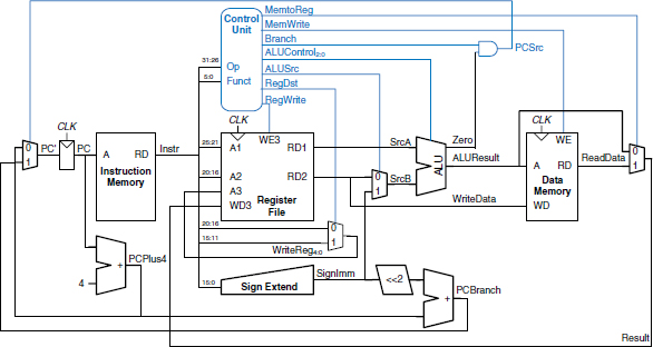
Figure 7.11 Complete single-cycle MIPS processor
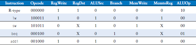
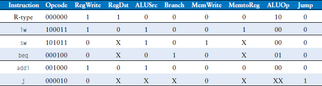
Most of the control information comes from the opcode, but R-type instructions also use the funct field to determine the ALU operation. Thus, we will simplify our design by factoring the control unit into two blocks of combinational logic, as shown in Figure 7.12. The main decoder computes most of the outputs from the opcode. It also determines a 2-bit ALUOp signal. The ALU decoder uses this ALUOp signal in conjunction with the funct field to compute ALUControl. The meaning of the ALUOp signal is given in Table 7.1.

Figure 7.12 Control unit internal structure
| ALUOp | Meaning |
|---|---|
| 00 | add |
| 01 | subtract |
| 10 | look at funct field |
| 11 | n/a |
Table 7.2 is a truth table for the ALU decoder. Recall that the meanings of the three ALUControl signals were given in Table 5.1. Because ALUOp is never 11, the truth table can use don’t care’s X1 and 1X instead of 01 and 10 to simplify the logic. When ALUOp is 00 or 01, the ALU should add or subtract, respectively. When ALUOp is 10, the decoder examines the funct field to determine the ALUControl. Note that, for the R-type instructions we implement, the first two bits of the funct field are always 10, so we may ignore them to simplify the decoder.
The control signals for each instruction were described as we built the datapath. Table 7.3 is a truth table for the main decoder that summarizes the control signals as a function of the opcode. All R-type instructions use the same main decoder values; they differ only in the ALU decoder output. Recall that, for instructions that do not write to the register file (e.g., sw and beq), the RegDst and MemtoReg control signals are don’t cares (X); the address and data to the register write port do not matter because RegWrite is not asserted. The logic for the decoder can be designed using your favorite techniques for combinational logic design.
Table 7.2 ALU decoder truth table
| ALUOp | Funct | ALUControl |
|---|---|---|
| 00 | X | 010 (add) |
| X1 | X | 110 (subtract) |
| 1X | 100000 (add) |
010 (add) |
| 1X | 100010 (sub) |
110 (subtract) |
| 1X | 100100 (and) |
000 (and) |
| 1X | 100101 (or) |
001 (or) |
| 1X | 101010 (slt) |
111 (set less than) |
Table 7.3 Main decoder truth table

Example 7.1 SINGLE-CYCLE PROCESSOR OPERATION
Determine the values of the control signals and the portions of the datapath that are used when executing an or instruction.
Solution: Figure 7.13 illustrates the control signals and flow of data during execution of the or instruction. The PC points to the memory location holding the instruction, and the instruction memory fetches this instruction.
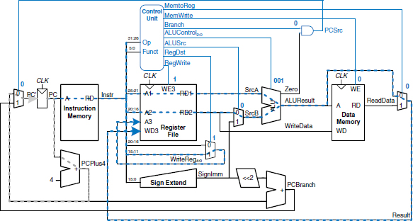
Figure 7.13 Control signals and data flow while executing or instruction
The main flow of data through the register file and ALU is represented with a dashed blue line. The register file reads the two source operands specified by Instr25:21 and Instr20:16. SrcB should come from the second port of the register file (not SignImm), so ALUSrc must be 0. or is an R-type instruction, so ALUOp is 10, indicating that ALUControl should be determined from the funct field to be 001. Result is taken from the ALU, so MemtoReg is 0. The result is written to the register file, so RegWrite is 1. The instruction does not write memory, so MemWrite = 0.
The selection of the destination register is also shown with a dashed blue line. The destination register is specified in the rd field, Instr15:11, so RegDst = 1.
The updating of the PC is shown with the dashed gray line. The instruction is not a branch, so Branch = 0 and, hence, PCSrc is also 0. The PC gets its next value from PCPlus4.
Note that data certainly does flow through the nonhighlighted paths, but that the value of that data is unimportant for this instruction. For example, the immediate is sign-extended and data is read from memory, but these values do not influence the next state of the system.
7.3.3 More Instructions
We have considered a limited subset of the full MIPS instruction set. Adding support for the addi and j instructions illustrates the principle of how to handle new instructions and also gives us a sufficiently rich instruction set to write many interesting programs. We will see that supporting some instructions simply requires enhancing the main decoder, whereas supporting others also requires more hardware in the datapath.
Example 7.2 addi INSTRUCTION
The add immediate instruction, addi, adds the value in a register to the immediate and writes the result to another register. The datapath already is capable of this task. Determine the necessary changes to the controller to support addi.
Solution: All we need to do is add a new row to the main decoder truth table showing the control signal values for addi, as given in Table 7.4. The result should be written to the register file, so RegWrite = 1. The destination register is specified in the rt field of the instruction, so RegDst = 0. SrcB comes from the immediate, so ALUSrc = 1. The instruction is not a branch, nor does it write memory, so Branch = MemWrite = 0. The result comes from the ALU, not memory, so MemtoReg = 0. Finally, the ALU should add, so ALUOp = 00.
Table 7.4 Main decoder truth table enhanced to support addi
Example 7.3 j INSTRUCTION
The jump instruction, j, writes a new value into the PC. The two least significant bits of the PC are always 0, because the PC is word aligned (i.e., always a multiple of 4). The next 26 bits are taken from the jump address field in Instr25:0. The upper four bits are taken from the old value of the PC.
The existing datapath lacks hardware to compute PC’ in this fashion. Determine the necessary changes to both the datapath and controller to handle j.
Solution: First, we must add hardware to compute the next PC value, PC’, in the case of a j instruction and a multiplexer to select this next PC, as shown in Figure 7.14. The new multiplexer uses the new Jump control signal.
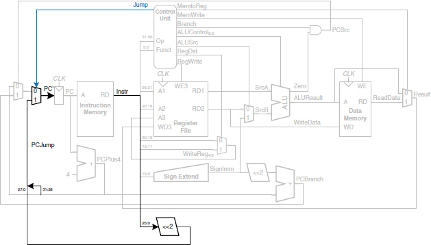
Figure 7.14 Single-cycle MIPS datapath enhanced to support the j instruction
Now we must add a row to the main decoder truth table for the j instruction and a column for the Jump signal, as shown in Table 7.5. The Jump control signal is 1 for the j instruction and 0 for all others. j does not write the register file or memory, so RegWrite = MemWrite = 0. Hence, we don’t care about the computation done in the datapath, and RegDst = ALUSrc = Branch = MemtoReg = ALUOp = X.
Table 7.5 Main decoder truth table enhanced to support j
7.3.4 Performance Analysis
Each instruction in the single-cycle processor takes one clock cycle, so the CPI is 1. The critical path for the lw instruction is shown in Figure 7.15 with a heavy dashed blue line. It starts with the PC loading a new address on the rising edge of the clock. The instruction memory reads the next instruction. The register file reads SrcA. While the register file is reading, the immediate field is sign-extended and selected at the ALUSrc multiplexer to determine SrcB. The ALU adds SrcA and SrcB to find the effective address. The data memory reads from this address. The MemtoReg multiplexer selects ReadData. Finally, Result must setup at the register file before the next rising clock edge, so that it can be properly written. Hence, the cycle time is
![]()
In most implementation technologies, the ALU, memory, and register file accesses are substantially slower than other operations. Therefore, the cycle time simplifies to
![]()
The numerical values of these times will depend on the specific implementation technology.

Figure 7.15 Critical path for lw instruction
Other instructions have shorter critical paths. For example, R-type instructions do not need to access data memory. However, we are disciplining ourselves to synchronous sequential design, so the clock period is constant and must be long enough to accommodate the slowest instruction.
Example 7.4 SINGLE-CYCLE PROCESSOR PERFORMANCE
Ben Bitdiddle is contemplating building the single-cycle MIPS processor in a 65 nm CMOS manufacturing process. He has determined that the logic elements have the delays given in Table 7.6. Help him compare the execution time for a program with 100 billion instructions.
Table 7.6 Delays of circuit elements
| Element | Parameter | Delay (ps) |
|---|---|---|
| register clk-to-Q | tpcq | 30 |
| register setup | tsetup | 20 |
| multiplexer | tmux | 25 |
| ALU | tALU | 200 |
| memory read | tmem | 250 |
| register file read | tRFread | 150 |
| register file setup | tRFsetup | 20 |
Solution: According to Equation 7.3, the cycle time of the single-cycle processor is Tc1 = 30 + 2(250) + 150 + 2(25) + 200 + 20 = 950 ps. We use the subscript “1” to distinguish it from subsequent processor designs. According to Equation 7.1, the total execution time is T1 = (100 X 109 instructions)(1 cycle/instruction) (950 X 10-12 s/cycle) = 95 seconds.
7.4 MULTICYCLE PROCESSOR
The single-cycle processor has three primary weaknesses. First, it requires a clock cycle long enough to support the slowest instruction (lw), even though most instructions are faster. Second, it requires three adders (one in the ALU and two for the PC logic); adders are relatively expensive circuits, especially if they must be fast. And third, it has separate instruction and data memories, which may not be realistic. Most computers have a single large memory that holds both instructions and data and that can be read and written.
The multicycle processor addresses these weaknesses by breaking an instruction into multiple shorter steps. In each short step, the processor can read or write the memory or register file or use the ALU. Different instructions use different numbers of steps, so simpler instructions can complete faster than more complex ones. The processor needs only one adder; this adder is reused for different purposes on various steps. And the processor uses a combined memory for instructions and data. The instruction is fetched from memory on the first step, and data may be read or written on later steps.
We design a multicycle processor following the same procedure we used for the single-cycle processor. First, we construct a datapath by connecting the architectural state elements and memories with combinational logic. But, this time, we also add nonarchitectural state elements to hold intermediate results between the steps. Then we design the controller. The controller produces different signals on different steps during execution of a single instruction, so it is now a finite state machine rather than combinational logic. We again examine how to add new instructions to the processor. Finally, we analyze the performance of the multicycle processor and compare it to the single-cycle processor.
7.4.1 Multicycle Datapath
Again, we begin our design with the memory and architectural state of the MIPS processor, shown in Figure 7.16. In the single-cycle design, we used separate instruction and data memories because we needed to read the instruction memory and read or write the data memory all in one cycle. Now, we choose to use a combined memory for both instructions and data. This is more realistic, and it is feasible because we can read the instruction in one cycle, then read or write the data in a separate cycle. The PC and register file remain unchanged. We gradually build the datapath by adding components to handle each step of each instruction. The new connections are emphasized in black (or blue, for new control signals), whereas the hardware that has already been studied is shown in gray.

Figure 7.16 State elements with unified instruction/data memory
The PC contains the address of the instruction to execute. The first step is to read this instruction from instruction memory. Figure 7.17 shows that the PC is simply connected to the address input of the instruction memory. The instruction is read and stored in a new nonarchitectural Instruction Register so that it is available for future cycles. The Instruction Register receives an enable signal, called IRWrite, that is asserted when it should be updated with a new instruction.
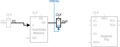
Figure 7.17 Fetch instruction from memory
As we did with the single-cycle processor, we will work out the datapath connections for the lw instruction. Then we will enhance the datapath to handle the other instructions. For a lw instruction, the next step is to read the source register containing the base address. This register is specified in the rs field of the instruction, Instr25:21. These bits of the instruction are connected to one of the address inputs, A1, of the register file, as shown in Figure 7.18. The register file reads the register onto RD1. This value is stored in another nonarchitectural register, A.

Figure 7.18 Read source operand from register file
The lw instruction also requires an offset. The offset is stored in the immediate field of the instruction, Instr15:0 and must be sign-extended to 32 bits, as shown in Figure 7.19. The 32-bit sign-extended value is called SignImm. To be consistent, we might store SignImm in another nonarchitectural register. However, SignImm is a combinational function of Instr and will not change while the current instruction is being processed, so there is no need to dedicate a register to hold the constant value.

Figure 7.19 Sign-extend the immediate
The address of the load is the sum of the base address and offset. We use an ALU to compute this sum, as shown in Figure 7.20. ALUControl should be set to 010 to perform an addition. ALUResult is stored in a nonarchitectural register called ALUOut.
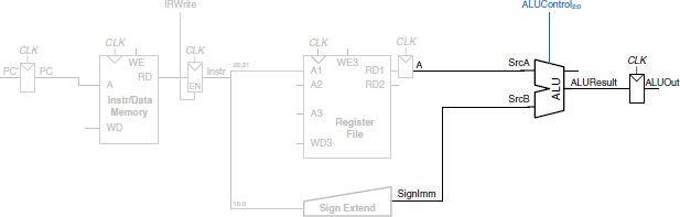
Figure 7.20 Add base address to offset
The next step is to load the data from the calculated address in the memory. We add a multiplexer in front of the memory to choose the memory address, Adr, from either the PC or ALUOut, as shown in Figure 7.21. The multiplexer select signal is called IorD, to indicate either an instruction or data address. The data read from the memory is stored in another nonarchitectural register, called Data. Notice that the address multiplexer permits us to reuse the memory during the lw instruction. On the first step, the address is taken from the PC to fetch the instruction. On a later step, the address is taken from ALUOut to load the data. Hence, IorD must have different values on different steps. In Section 7.4.2, we develop the FSM controller that generates these sequences of control signals.

Figure 7.21 Load data from memory
Finally, the data is written back to the register file, as shown in Figure 7.22. The destination register is specified by the rt field of the instruction, Instr20:16.

Figure 7.22 Write data back to register file
While all this is happening, the processor must update the program counter by adding 4 to the old PC. In the single-cycle processor, a separate adder was needed. In the multicycle processor, we can use the existing ALU on one of the steps when it is not busy. To do so, we must insert source multiplexers to choose the PC and the constant 4 as ALU inputs, as shown in Figure 7.23. A two-input multiplexer controlled by ALUSrcA chooses either the PC or register A as SrcA. A four-input multiplexer controlled by ALUSrcB chooses either 4 or SignImm as SrcB. We use the other two multiplexer inputs later when we extend the datapath to handle other instructions. (The numbering of inputs to the multiplexer is arbitrary.) To update the PC, the ALU adds SrcA (PC) to SrcB (4), and the result is written into the program counter register. The PCWrite control signal enables the PC register to be written only on certain cycles.

Figure 7.23 Increment PC by 4
This completes the datapath for the lw instruction. Next, let us extend the datapath to also handle the sw instruction. Like the lw instruction, the sw instruction reads a base address from port 1 of the register file and sign-extends the immediate. The ALU adds the base address to the immediate to find the memory address. All of these functions are already supported by existing hardware in the datapath.
The only new feature of sw is that we must read a second register from the register file and write it into the memory, as shown in Figure 7.24. The register is specified in the rt field of the instruction, Instr20:16, which is connected to the second port of the register file. When the register is read, it is stored in a nonarchitectural register, B. On the next step, it is sent to the write data port (WD) of the data memory to be written. The memory receives an additional MemWrite control signal to indicate that the write should occur.

Figure 7.24 Enhanced datapath for sw instruction
For R-type instructions, the instruction is again fetched, and the two source registers are read from the register file. Another input of the SrcB multiplexer is used to choose register B as the second source register for the ALU, as shown in Figure 7.25. The ALU performs the appropriate operation and stores the result in ALUOut. On the next step, ALUOut is written back to the register specified by the rd field of the instruction, Instr15:11. This requires two new multiplexers. The MemtoReg multiplexer selects whether WD3 comes from ALUOut (for R-type instructions) or from Data (for lw). The RegDst instruction selects whether the destination register is specified in the rt or rd field of the instruction.

Figure 7.25 Enhanced datapath for R-type instructions
For the beq instruction, the instruction is again fetched, and the two source registers are read from the register file. To determine whether the registers are equal, the ALU subtracts the registers and examines the Zero flag. Meanwhile, the datapath must compute the next value of the PC if the branch is taken: PC’ = PC + 4 + SignImm X 4. In the single-cycle processor, yet another adder was needed to compute the branch address. In the multicycle processor, the ALU can be reused again to save hardware. On one step, the ALU computes PC + 4 and writes it back to the program counter, as was done for other instructions. On another step, the ALU uses this updated PC value to compute PC + SignImm X 4. SignImm is left-shifted by 2 to multiply it by 4, as shown in Figure 7.26. The SrcB multiplexer chooses this value and adds it to the PC. This sum represents the destination of the branch and is stored in ALUOut. A new multiplexer, controlled by PCSrc, chooses what signal should be sent to PC’. The program counter should be written either when PCWrite is asserted or when a branch is taken. A new control signal, Branch, indicates that the beq instruction is being executed. The branch is taken if Zero is also asserted. Hence, the datapath computes a new PC write enable, called PCEn, which is TRUE either when PCWrite is asserted or when both Branch and Zero are asserted.

Figure 7.26 Enhanced datapath for beq instruction
This completes the design of the multicycle MIPS processor datapath. The design process is much like that of the single-cycle processor in that hardware is systematically connected between the state elements to handle each instruction. The main difference is that the instruction is executed in several steps. Nonarchitectural registers are inserted to hold the results of each step. In this way, the ALU can be reused several times, saving the cost of extra adders. Similarly, the instructions and data can be stored in one shared memory. In the next section, we develop an FSM controller to deliver the appropriate sequence of control signals to the datapath on each step of each instruction.
7.4.2 Multicycle Control
As in the single-cycle processor, the control unit computes the control signals based on the opcode and funct fields of the instruction, Instr31:26 and Instr5:0. Figure 7.27 shows the entire multicycle MIPS processor with the control unit attached to the datapath. The datapath is shown in black, and the control unit is shown in blue.

Figure 7.27 Complete multicycle MIPS processor
As in the single-cycle processor, the control unit is partitioned into a main controller and an ALU decoder, as shown in Figure 7.28. The ALU decoder is unchanged and follows the truth table of Table 7.2. Now, however, the main controller is an FSM that applies the proper control signals on the proper cycles or steps. The sequence of control signals depends on the instruction being executed. In the remainder of this section, we will develop the FSM state transition diagram for the main controller.

Figure 7.28 Control unit internal structure
The main controller produces multiplexer select and register enable signals for the datapath. The select signals are MemtoReg, RegDst, IorD, PCSrc, ALUSrcB, and ALUSrcA. The enable signals are IRWrite, MemWrite, PCWrite, Branch, and RegWrite.
To keep the following state transition diagrams readable, only the relevant control signals are listed. Select signals are listed only when their value matters; otherwise, they are don’t cares. Enable signals are listed only when they are asserted; otherwise, they are 0.
The first step for any instruction is to fetch the instruction from memory at the address held in the PC. The FSM enters this state on reset. To read memory, IorD = 0, so the address is taken from the PC. IRWrite is asserted to write the instruction into the instruction register, IR. Meanwhile, the PC should be incremented by 4 to point to the next instruction. Because the ALU is not being used for anything else, the processor can use it to compute PC + 4 at the same time that it fetches the instruction. ALUSrcA = 0, so SrcA comes from the PC. ALUSrcB = 01, so SrcB is the constant 4. ALUOp = 00, so the ALU decoder produces ALUControl = 010 to make the ALU add. To update the PC with this new value, PCSrc = 0, and PCWrite is asserted. These control signals are shown in Figure 7.29. The data flow on this step is shown in Figure 7.30, with the instruction fetch shown using the dashed blue line and the PC increment shown using the dashed gray line.
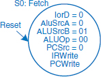
Figure 7.29 Fetch
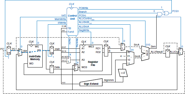
Figure 7.30 Data flow during the fetch step
The next step is to read the register file and decode the instruction. The register file always reads the two sources specified by the rs and rt fields of the instruction. Meanwhile, the immediate is sign-extended. Decoding involves examining the opcode of the instruction to determine what to do next. No control signals are necessary to decode the instruction, but the FSM must wait 1 cycle for the reading and decoding to complete, as shown in Figure 7.31. The new state is highlighted in blue. The data flow is shown in Figure 7.32.

Figure 7.31 Decode

Figure 7.32 Data flow during the decode step
Now the FSM proceeds to one of several possible states, depending on the opcode. If the instruction is a memory load or store (lw or sw), the multicycle processor computes the address by adding the base address to the sign-extended immediate. This requires ALUSrcA = 1 to select register A and ALUSrcB = 10 to select SignImm. ALUOp = 00, so the ALU adds. The effective address is stored in the ALUOut register for use on the next step. This FSM step is shown in Figure 7.33, and the data flow is shown in Figure 7.34.
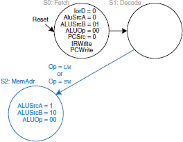
Figure 7.33 Memory address computation

Figure 7.34 Data flow during memory address computation
If the instruction is lw, the multicycle processor must next read data from memory and write it to the register file. These two steps are shown in Figure 7.35. To read from memory, IorD = 1 to select the memory address that was just computed and saved in ALUOut. This address in memory is read and saved in the Data register during step S3. On the next step, S4, Data is written to the register file. MemtoReg = 1 to select Data, and RegDst = 0 to pull the destination register from the rt field of the instruction. RegWrite is asserted to perform the write, completing the lw instruction. Finally, the FSM returns to the initial state, S0, to fetch the next instruction. For these and subsequent steps, try to visualize the data flow on your own.

Figure 7.35 Memory read
From state S2, if the instruction is sw, the data read from the second port of the register file is simply written to memory. IorD = 1 to select the address computed in S2 and saved in ALUOut. MemWrite is asserted to write the memory. Again, the FSM returns to S0 to fetch the next instruction. The added step is shown in Figure 7.36.
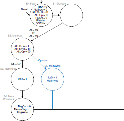
Figure 7.36 Memory write
If the opcode indicates an R-type instruction, the multicycle processor must calculate the result using the ALU and write that result to the register file. Figure 7.37 shows these two steps. In S6, the instruction is executed by selecting the A and B registers (ALUSrcA = 1, ALUSrcB = 00) and performing the ALU operation indicated by the funct field of the instruction. ALUOp = 10 for all R-type instructions. The ALUResult is stored in ALUOut. In S7, ALUOut is written to the register file, RegDst = 1, because the destination register is specified in the rd field of the instruction. MemtoReg = 0 because the write data, WD3, comes from ALUOut. RegWrite is asserted to write the register file.

Figure 7.37 Execute R-type operation
For a beq instruction, the processor must calculate the destination address and compare the two source registers to determine whether the branch should be taken. This requires two uses of the ALU and hence might seem to demand two new states. Notice, however, that the ALU was not used during S1 when the registers were being read. The processor might as well use the ALU at that time to compute the destination address by adding the incremented PC, PC + 4, to SignImm X 4, as shown in Figure 7.38 (see page 396). ALUSrcA = 0 to select the incremented PC, ALUSrcB = 11 to select SignImm X 4, and ALUOp = 00 to add. The destination address is stored in ALUOut. If the instruction is not beq, the computed address will not be used in subsequent cycles, but its computation was harmless. In S8, the processor compares the two registers by subtracting them and checking to determine whether the result is 0. If it is, the processor branches to the address that was just computed. ALUSrcA = 1 to select register A; ALUSrcB = 00 to select register B; ALUOp = 01 to subtract; PCSrc = 1 to take the destination address from ALUOut, and Branch = 1 to update the PC with this address if the ALU result is 0.2

Figure 7.38 Branch
Putting these steps together, Figure 7.39 shows the complete main controller state transition diagram for the multicycle processor (see page 397). Converting it to hardware is a straightforward but tedious task using the techniques of Chapter 3. Better yet, the FSM can be coded in an HDL and synthesized using the techniques of Chapter 4.
Figure 7.39 Complete multicycle control FSM
7.4.3 More Instructions
As we did in Section 7.3.3 for the single-cycle processor, let us now extend the multicycle processor to support the addi and j instructions. The next two examples illustrate the general design process to support new instructions.
Example 7.5 addi INSTRUCTION
Modify the multicycle processor to support addi.
Solution: The datapath is already capable of adding registers to immediates, so all we need to do is add new states to the main controller FSM for addi, as shown in Figure 7.40 (see page 398). The states are similar to those for R-type instructions. In S9, register A is added to SignImm (ALUSrcA = 1, ALUSrcB = 10, ALUOp = 00) and the result, ALUResult, is stored in ALUOut. In S10, ALUOut is written to the register specified by the rt field of the instruction (RegDst = 0, MemtoReg = 0, RegWrite asserted). The astute reader may notice that S2 and S9 are identical and could be merged into a single state.

Figure 7.40 Main controller states for addi
Example 7.6 j INSTRUCTION
Modify the multicycle processor to support j.
Solution: First, we must modify the datapath to compute the next PC value in the case of a j instruction. Then we add a state to the main controller to handle the instruction.
Figure 7.41 shows the enhanced datapath (see page 399). The jump destination address is formed by left-shifting the 26-bit addr field of the instruction by two bits, then prepending the four most significant bits of the already incremented PC. The PCSrc multiplexer is extended to take this address as a third input.
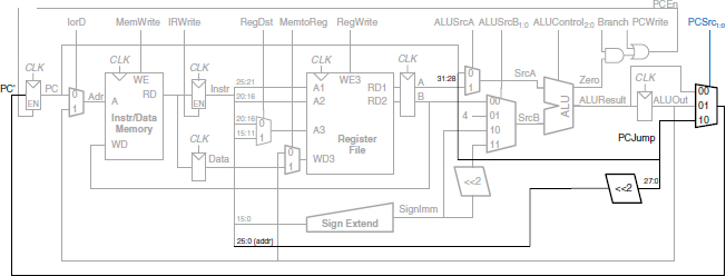
Figure 7.41 Multicycle MIPS datapath enhanced to support the j instruction
Figure 7.42 shows the enhanced main controller (see page 400). The new state, S11, simply selects PC’ as the PCJump value (PCSrc = 10) and writes the PC. Note that the PCSrc select signal is extended to two bits in S0 and S8 as well.
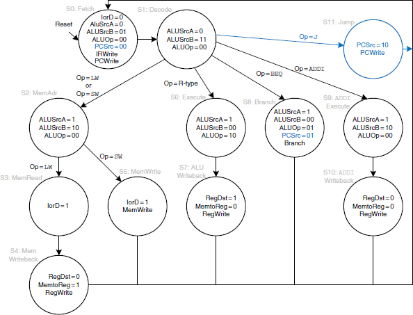
Figure 7.42 Main controller state for j
7.4.4 Performance Analysis
The execution time of an instruction depends on both the number of cycles it uses and the cycle time. Whereas the single-cycle processor performed all instructions in one cycle, the multicycle processor uses varying numbers of cycles for the various instructions. However, the multicycle processor does less work in a single cycle and, thus, has a shorter cycle time.
The multicycle processor requires three cycles for beq and j instructions, four cycles for sw, addi, and R-type instructions, and five cycles for lw instructions. The CPI depends on the relative likelihood that each instruction is used.
Example 7.7 MULTICYCLE PROCESSOR CPI
The SPECINT2000 benchmark consists of approximately 25% loads, 10% stores, 11% branches, 2% jumps, and 52% R-type instructions.3 Determine the average CPI for this benchmark.
Solution: The average CPI is the sum over each instruction of the CPI for that instruction multiplied by the fraction of the time that instruction is used. For this benchmark, Average CPI = (0.11 + 0.02)(3) + (0.52 + 0.10)(4) + (0.25)(5) = 4.12. This is better than the worst-case CPI of 5, which would be required if all instructions took the same time.
Recall that we designed the multicycle processor so that each cycle involved one ALU operation, memory access, or register file access. Let us assume that the register file is faster than the memory and that writing memory is faster than reading memory. Examining the datapath reveals two possible critical paths that would limit the cycle time:
![]()
The numerical values of these times will depend on the specific implementation technology.
Example 7.8 PROCESSOR PERFORMANCE COMPARISON
Ben Bitdiddle is wondering whether he would be better off building the multicycle processor instead of the single-cycle processor. For both designs, he plans on using a 65 nm CMOS manufacturing process with the delays given in Table 7.6. Help him compare each processor’s execution time for 100 billion instructions from the SPECINT2000 benchmark (see Example 7.7).
Solution: According to Equation 7.4, the cycle time of the multicycle processor is Tc2 = 30 + 25 + 250 + 20 = 325 ps. Using the CPI of 4.12 from Example 7.7, the total execution time is T2 = (100 X 109 instructions)(4.12 cycles/instruction) (325 X 10-12 s/cycle) = 133.9 seconds. According to Example 7.4, the single-cycle processor had a cycle time of Tc1 = 950 ps, a CPI of 1, and a total execution time of 95 seconds.
One of the original motivations for building a multicycle processor was to avoid making all instructions take as long as the slowest one. Unfortunately, this example shows that the multicycle processor is slower than the single-cycle processor given the assumptions of CPI and circuit element delays. The fundamental problem is that even though the slowest instruction, lw, was broken into five steps, the multicycle processor cycle time was not nearly improved fivefold. This is partly because not all of the steps are exactly the same length, and partly because the 50-ps sequencing overhead of the register clk-to-Q and setup time must now be paid on every step, not just once for the entire instruction. In general, engineers have learned that it is difficult to exploit the fact that some computations are faster than others unless the differences are large.
Compared with the single-cycle processor, the multicycle processor is likely to be less expensive because it eliminates two adders and combines the instruction and data memories into a single unit. It does, however, require five nonarchitectural registers and additional multiplexers.
7.5 PIPELINED PROCESSOR
Pipelining, introduced in Section 3.6, is a powerful way to improve the throughput of a digital system. We design a pipelined processor by subdividing the single-cycle processor into five pipeline stages. Thus, five instructions can execute simultaneously, one in each stage. Because each stage has only one-fifth of the entire logic, the clock frequency is almost five times faster. Hence, the latency of each instruction is ideally unchanged, but the throughput is ideally five times better. Microprocessors execute millions or billions of instructions per second, so throughput is more important than latency. Pipelining introduces some overhead, so the throughput will not be quite as high as we might ideally desire, but pipelining nevertheless gives such great advantage for so little cost that all modern high-performance microprocessors are pipelined.
Reading and writing the memory and register file and using the ALU typically constitute the biggest delays in the processor. We choose five pipeline stages so that each stage involves exactly one of these slow steps. Specifically, we call the five stages Fetch, Decode, Execute, Memory, and Writeback. They are similar to the five steps that the multicycle processor used to perform lw. In the Fetch stage, the processor reads the instruction from instruction memory. In the Decode stage, the processor reads the source operands from the register file and decodes the instruction to produce the control signals. In the Execute stage, the processor performs a computation with the ALU. In the Memory stage, the processor reads or writes data memory. Finally, in the Writeback stage, the processor writes the result to the register file, when applicable.
Figure 7.43 shows a timing diagram comparing the single-cycle and pipelined processors. Time is on the horizontal axis, and instructions are on the vertical axis. The diagram assumes the logic element delays from Table 7.6 but ignores the delays of multiplexers and registers. In the single-cycle processor, Figure 7.43(a), the first instruction is read from memory at time 0; next the operands are read from the register file; and then the ALU executes the necessary computation. Finally, the data memory may be accessed, and the result is written back to the register file by 950 ps. The second instruction begins when the first completes. Hence, in this diagram, the single-cycle processor has an instruction latency of 250 + 150 + 200 + 250 + 100 = 950 ps and a throughput of 1 instruction per 950 ps (1.05 billion instructions per second).

Figure 7.43 Timing diagrams: (a) single-cycle processor, (b) pipelined processor
In the pipelined processor, Figure 7.43(b), the length of a pipeline stage is set at 250 ps by the slowest stage, the memory access (in the Fetch or Memory stage). At time 0, the first instruction is fetched from memory. At 250 ps, the first instruction enters the Decode stage, and a second instruction is fetched. At 500 ps, the first instruction executes, the second instruction enters the Decode stage, and a third instruction is fetched. And so forth, until all the instructions complete. The instruction latency is 5 X 250 = 1250 ps. The throughput is 1 instruction per 250 ps (4 billion instructions per second). Because the stages are not perfectly balanced with equal amounts of logic, the latency is slightly longer for the pipelined than for the single-cycle processor. Similarly, the throughput is not quite five times as great for a five-stage pipeline as for the single-cycle processor. Nevertheless, the throughput advantage is substantial.
Figure 7.44 shows an abstracted view of the pipeline in operation in which each stage is represented pictorially. Each pipeline stage is represented with its major component—instruction memory (IM), register file (RF) read, ALU execution, data memory (DM), and register file writeback—to illustrate the flow of instructions through the pipeline. Reading across a row shows the clock cycles in which a particular instruction is in each stage. For example, the sub instruction is fetched in cycle 3 and executed in cycle 5. Reading down a column shows what the various pipeline stages are doing on a particular cycle. For example, in cycle 6, the or instruction is being fetched from instruction memory, while $s1 is being read from the register file, the ALU is computing $t5 AND $t6, the data memory is idle, and the register file is writing a sum to $s3. Stages are shaded to indicate when they are used. For example, the data memory is used by lw in cycle 4 and by sw in cycle 8. The instruction memory and ALU are used in every cycle. The register file is written by every instruction except sw. We assume that in the pipelined processor, the register file is written in the first part of a cycle and read in the second part, as suggested by the shading. This way, data can be written and read back within a single cycle.

Figure 7.44 Abstract view of pipeline in operation
A central challenge in pipelined systems is handling hazards that occur when the results of one instruction are needed by a subsequent instruction before the former instruction has completed. For example, if the add in Figure 7.44 used $s2 rather than $t2, a hazard would occur because the $s2 register has not been written by the lw by the time it is read by the add. This section explores forwarding, stalls, and flushes as methods to resolve hazards. Finally, this section revisits performance analysis considering sequencing overhead and the impact of hazards.
7.5.1 Pipelined Datapath
The pipelined datapath is formed by chopping the single-cycle datapath into five stages separated by pipeline registers. Figure 7.45(a) shows the single-cycle datapath stretched out to leave room for the pipeline registers. Figure 7.45(b) shows the pipelined datapath formed by inserting four pipeline registers to separate the datapath into five stages. The stages and their boundaries are indicated in blue. Signals are given a suffix (F, D, E, M, or W) to indicate the stage in which they reside.

Figure 7.45 Single-cycle and pipelined datapaths
The register file is peculiar because it is read in the Decode stage and written in the Writeback stage. It is drawn in the Decode stage, but the write address and data come from the Writeback stage. This feedback will lead to pipeline hazards, which are discussed in Section 7.5.3.
One of the subtle but critical issues in pipelining is that all signals associated with a particular instruction must advance through the pipeline in unison. Figure 7.45(b) has an error related to this issue. Can you find it?
The error is in the register file write logic, which should operate in the Writeback stage. The data value comes from ResultW, a Writeback stage signal. But the address comes from WriteRegE, an Execute stage signal. In the pipeline diagram of Figure 7.44, during cycle 5, the result of the lw instruction would be incorrectly written to register $s4 rather than $s2.
Figure 7.46 shows a corrected datapath. The WriteReg signal is now pipelined along through the Memory and Writeback stages, so it remains in sync with the rest of the instruction. WriteRegW and ResultW are fed back together to the register file in the Writeback stage.

Figure 7.46 Corrected pipelined datapath
The astute reader may notice that the PC’ logic is also problematic, because it might be updated with a Fetch or a Memory stage signal (PCPlus4F or PCBranchM). This control hazard will be fixed in Section 7.5.3.
7.5.2 Pipelined Control
The pipelined processor takes the same control signals as the single-cycle processor and therefore uses the same control unit. The control unit examines the opcode and funct fields of the instruction in the Decode stage to produce the control signals, as was described in Section 7.3.2. These control signals must be pipelined along with the data so that they remain synchronized with the instruction.
The entire pipelined processor with control is shown in Figure 7.47. RegWrite must be pipelined into the Writeback stage before it feeds back to the register file, just as WriteReg was pipelined in Figure 7.46.

Figure 7.47 Pipelined processor with control
7.5.3 Hazards
In a pipelined system, multiple instructions are handled concurrently. When one instruction is dependent on the results of another that has not yet completed, a hazard occurs.
The register file can be read and written in the same cycle. Let us assume that the write takes place during the first half of the cycle and the read takes place during the second half of the cycle, so that a register can be written and read back in the same cycle without introducing a hazard.
Figure 7.48 illustrates hazards that occur when one instruction writes a register ($s0) and subsequent instructions read this register. This is called a read after write (RAW) hazard. The add instruction writes a result into $s0 in the first half of cycle 5. However, the and instruction reads $s0 on cycle 3, obtaining the wrong value. The or instruction reads $s0 on cycle 4, again obtaining the wrong value. The sub instruction reads $s0 in the second half of cycle 5, obtaining the correct value, which was written in the first half of cycle 5. Subsequent instructions also read the correct value of $s0. The diagram shows that hazards may occur in this pipeline when an instruction writes a register and either of the two subsequent instructions read that register. Without special treatment, the pipeline will compute the wrong result.

Figure 7.48 Abstract pipeline diagram illustrating hazards
On closer inspection, however, observe that the sum from the add instruction is computed by the ALU in cycle 3 and is not strictly needed by the and instruction until the ALU uses it in cycle 4. In principle, we should be able to forward the result from one instruction to the next to resolve the RAW hazard without slowing down the pipeline. In other situations explored later in this section, we may have to stall the pipeline to give time for a result to be computed before the subsequent instruction uses the result. In any event, something must be done to solve hazards so that the program executes correctly despite the pipelining.
Hazards are classified as data hazards or control hazards. A data hazard occurs when an instruction tries to read a register that has not yet been written back by a previous instruction. A control hazard occurs when the decision of what instruction to fetch next has not been made by the time the fetch takes place. In the remainder of this section, we will enhance the pipelined processor with a hazard unit that detects hazards and handles them appropriately, so that the processor executes the program correctly.
Solving Data Hazards with Forwarding
Some data hazards can be solved by forwarding (also called bypassing) a result from the Memory or Writeback stage to a dependent instruction in the Execute stage. This requires adding multiplexers in front of the ALU to select the operand from either the register file or the Memory or Writeback stage. Figure 7.49 illustrates this principle. In cycle 4, $s0 is forwarded from the Memory stage of the add instruction to the Execute stage of the dependent and instruction. In cycle 5, $s0 is forwarded from the Writeback stage of the add instruction to the Execute stage of the dependent or instruction.
Forwarding is necessary when an instruction in the Execute stage has a source register matching the destination register of an instruction in the Memory or Writeback stage. Figure 7.50 modifies the pipelined processor to support forwarding. It adds a hazard detection unit and two forwarding multiplexers. The hazard detection unit receives the two source registers from the instruction in the Execute stage and the destination registers from the instructions in the Memory and Writeback stages. It also receives the RegWrite signals from the Memory and Writeback stages to know whether the destination register will actually be written (for example, the sw and beq instructions do not write results to the register file and hence do not need to have their results forwarded). Note that the RegWrite signals are connected by name. In other words, rather than cluttering up the diagram with long wires running from the control signals at the top to the hazard unit at the bottom, the connections are indicated by a short stub of wire labeled with the control signal name to which it is connected.

Figure 7.49 Abstract pipeline diagram illustrating forwarding

Figure 7.50 Pipelined processor with forwarding to solve hazards
The hazard detection unit computes control signals for the forwarding multiplexers to choose operands from the register file or from the results in the Memory or Writeback stage. It should forward from a stage if that stage will write a destination register and the destination register matches the source register. However, $0 is hardwired to 0 and should never be forwarded. If both the Memory and Writeback stages contain matching destination registers, the Memory stage should have priority, because it contains the more recently executed instruction. In summary, the function of the forwarding logic for SrcA is given below. The forwarding logic for SrcB (ForwardBE) is identical except that it checks rt rather than rs.

Solving Data Hazards with Stalls
Forwarding is sufficient to solve RAW data hazards when the result is computed in the Execute stage of an instruction, because its result can then be forwarded to the Execute stage of the next instruction. Unfortunately, the lw instruction does not finish reading data until the end of the Memory stage, so its result cannot be forwarded to the Execute stage of the next instruction. We say that the lw instruction has a two-cycle latency, because a dependent instruction cannot use its result until two cycles later. Figure 7.51 shows this problem. The lw instruction receives data from memory at the end of cycle 4. But the and instruction needs that data as a source operand at the beginning of cycle 4. There is no way to solve this hazard with forwarding.
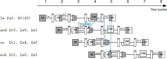
Figure 7.51 Abstract pipeline diagram illustrating trouble forwarding from lw
The alternative solution is to stall the pipeline, holding up operation until the data is available. Figure 7.52 shows stalling the dependent instruction (and) in the Decode stage. and enters the Decode stage in cycle 3 and stalls there through cycle 4. The subsequent instruction (or) must remain in the Fetch stage during both cycles as well, because the Decode stage is full.

Figure 7.52 Abstract pipeline diagram illustrating stall to solve hazards
In cycle 5, the result can be forwarded from the Writeback stage of lw to the Execute stage of and. In cycle 6, source $s0 of the or instruction is read directly from the register file, with no need for forwarding.
Notice that the Execute stage is unused in cycle 4. Likewise, Memory is unused in Cycle 5 and Writeback is unused in cycle 6. This unused stage propagating through the pipeline is called a bubble, and it behaves like a nop instruction. The bubble is introduced by zeroing out the Execute stage control signals during a Decode stall so that the bubble performs no action and changes no architectural state.
In summary, stalling a stage is performed by disabling the pipeline register, so that the contents do not change. When a stage is stalled, all previous stages must also be stalled, so that no subsequent instructions are lost. The pipeline register directly after the stalled stage must be cleared to prevent bogus information from propagating forward. Stalls degrade performance, so they should only be used when necessary.
Figure 7.53 modifies the pipelined processor to add stalls for lw data dependencies. The hazard unit examines the instruction in the Execute stage. If it is lw and its destination register (rtE) matches either source operand of the instruction in the Decode stage (rsD or rtD), that instruction must be stalled in the Decode stage until the source operand is ready.

Figure 7.53 Pipelined processor with stalls to solve lw data hazard
Stalls are supported by adding enable inputs (EN) to the Fetch and Decode pipeline registers and a synchronous reset/clear (CLR) input to the Execute pipeline register. When a lw stall occurs, StallD and StallF are asserted to force the Decode and Fetch stage pipeline registers to hold their old values. FlushE is also asserted to clear the contents of the Execute stage pipeline register, introducing a bubble.4
The MemtoReg signal is asserted for the lw instruction. Hence, the logic to compute the stalls and flushes is
lwstall = ((rsD == rtE) OR (rtD == rtE)) AND MemtoRegE
StallF = StallD = FlushE = lwstall
Solving Control Hazards
The beq instruction presents a control hazard: the pipelined processor does not know what instruction to fetch next, because the branch decision has not been made by the time the next instruction is fetched.
One mechanism for dealing with the control hazard is to stall the pipeline until the branch decision is made (i.e., PCSrc is computed). Because the decision is made in the Memory stage, the pipeline would have to be stalled for three cycles at every branch. This would severely degrade the system performance.
An alternative is to predict whether the branch will be taken and begin executing instructions based on the prediction. Once the branch decision is available, the processor can throw out the instructions if the prediction was wrong. In particular, suppose that we predict that branches are not taken and simply continue executing the program in order. If the branch should have been taken, the three instructions following the branch must be flushed (discarded) by clearing the pipeline registers for those instructions. These wasted instruction cycles are called the branch misprediction penalty.
Figure 7.54 shows such a scheme, in which a branch from address 20 to address 64 is taken. The branch decision is not made until cycle 4, by which point the and, or, and sub instructions at addresses 24, 28, and 2C have already been fetched. These instructions must be flushed, and the slt instruction is fetched from address 64 in cycle 5. This is somewhat of an improvement, but flushing so many instructions when the branch is taken still degrades performance.

Figure 7.54 Abstract pipeline diagram illustrating flushing when a branch is taken
We could reduce the branch misprediction penalty if the branch decision could be made earlier. Making the decision simply requires comparing the values of two registers. Using a dedicated equality comparator is much faster than performing a subtraction and zero detection. If the comparator is fast enough, it could be moved back into the Decode stage, so that the operands are read from the register file and compared to determine the next PC by the end of the Decode stage.
Figure 7.55 shows the pipeline operation with the early branch decision being made in cycle 2. In cycle 3, the and instruction is flushed and the slt instruction is fetched. Now the branch misprediction penalty is reduced to only one instruction rather than three.

Figure 7.55 Abstract pipeline diagram illustrating earlier branch decision
Figure 7.56 modifies the pipelined processor to move the branch decision earlier and handle control hazards. An equality comparator is added to the Decode stage and the PCSrc AND gate is moved earlier, so that PCSrc can be determined in the Decoder stage rather than the Memory stage. The PCBranch adder must also be moved into the Decode stage so that the destination address can be computed in time. The synchronous clear input (CLR) connected to PCSrcD is added to the Decode stage pipeline register so that the incorrectly fetched instruction can be flushed when a branch is taken.
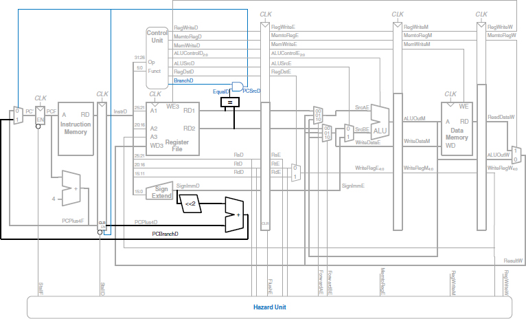
Figure 7.56 Pipelined processor handling branch control hazard
Unfortunately, the early branch decision hardware introduces a new RAW data hazard. Specifically, if one of the source operands for the branch was computed by a previous instruction and has not yet been written into the register file, the branch will read the wrong operand value from the register file. As before, we can solve the data hazard by forwarding the correct value if it is available or by stalling the pipeline until the data is ready.
Figure 7.57 shows the modifications to the pipelined processor needed to handle the Decode stage data dependency. If a result is in the Writeback stage, it will be written in the first half of the cycle and read during the second half, so no hazard exists. If the result of an ALU instruction is in the Memory stage, it can be forwarded to the equality comparator through two new multiplexers. If the result of an ALU instruction is in the Execute stage or the result of a lw instruction is in the Memory stage, the pipeline must be stalled at the Decode stage until the result is ready.

Figure 7.57 Pipelined processor handling data dependencies for branch instructions
The function of the Decode stage forwarding logic is given below.
ForwardAD = (rsD ! = 0) AND (rsD == WriteRegM) AND RegWriteM
ForwardBD = (rtD ! = 0) AND (rtD == WriteRegM) AND RegWriteM
The function of the stall detection logic for a branch is given below. The processor must make a branch decision in the Decode stage. If either of the sources of the branch depends on an ALU instruction in the Execute stage or on a lw instruction in the Memory stage, the processor must stall until the sources are ready.
branchstall =
BranchD AND RegWriteE AND (WriteRegE == rsD OR WriteRegE == rtD)
OR
BranchD AND MemtoRegM AND (WriteRegM == rsD OR WriteRegM == rtD)
Now the processor might stall due to either a load or a branch hazard:
StallF = StallD = FlushE = lwstall OR branchstall
Hazard Summary
In summary, RAW data hazards occur when an instruction depends on the result of another instruction that has not yet been written into the register file. The data hazards can be resolved by forwarding if the result is computed soon enough; otherwise, they require stalling the pipeline until the result is available. Control hazards occur when the decision of what instruction to fetch has not been made by the time the next instruction must be fetched. Control hazards are solved by predicting which instruction should be fetched and flushing the pipeline if the prediction is later determined to be wrong. Moving the decision as early as possible minimizes the number of instructions that are flushed on a misprediction. You may have observed by now that one of the challenges of designing a pipelined processor is to understand all the possible interactions between instructions and to discover all the hazards that may exist. Figure 7.58 shows the complete pipelined processor handling all of the hazards.
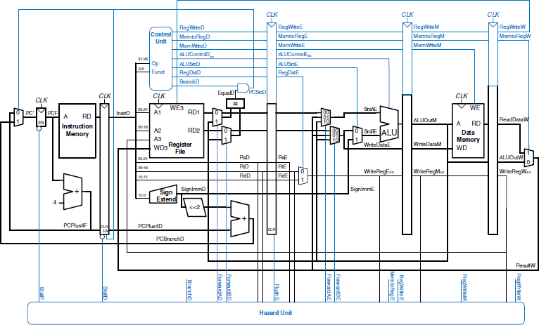
Figure 7.58 Pipelined processor with full hazard handling
7.5.4 More Instructions
Supporting new instructions in the pipelined processor is much like supporting them in the single-cycle processor. However, new instructions may introduce hazards that must be detected and solved.
In particular, supporting addi and j instructions on the pipelined processor requires enhancing the controller, exactly as was described in Section 7.3.3, and adding a jump multiplexer to the datapath after the branch multiplexer. Like a branch, the jump takes place in the Decode stage, so the subsequent instruction in the Fetch stage must be flushed. Designing this flush logic is left as Exercise 7.29.
7.5.5 Performance Analysis
The pipelined processor ideally would have a CPI of 1, because a new instruction is issued every cycle. However, a stall or a flush wastes a cycle, so the CPI is slightly higher and depends on the specific program being executed.
Example 7.9 PIPELINED PROCESSOR CPI
The SPECINT2000 benchmark considered in Example 7.7 consists of approximately 25% loads, 10% stores, 11% branches, 2% jumps, and 52% R-type instructions. Assume that 40% of the loads are immediately followed by an instruction that uses the result, requiring a stall, and that one quarter of the branches are mispredicted, requiring a flush. Assume that jumps always flush the subsequent instruction. Ignore other hazards. Compute the average CPI of the pipelined processor.
Solution: The average CPI is the sum over each instruction of the CPI for that instruction multiplied by the fraction of time that instruction is used. Loads take one clock cycle when there is no dependency and two cycles when the processor must stall for a dependency, so they have a CPI of (0.6)(1) + (0.4)(2) = 1.4. Branches take one clock cycle when they are predicted properly and two when they are not, so they have a CPI of (0.75)(1) + (0.25)(2) = 1.25. Jumps always have a CPI of 2. All other instructions have a CPI of 1. Hence, for this benchmark, Average CPI = (0.25)(1.4) + (0.1)(1) + (0.11)(1.25) + (0.02)(2) + (0.52)(1) = 1.15.
We can determine the cycle time by considering the critical path in each of the five pipeline stages shown in Figure 7.58. Recall that the register file is written in the first half of the Writeback cycle and read in the second half of the Decode cycle. Therefore, the cycle time of the Decode and Writeback stages is twice the time necessary to do the half-cycle of work.
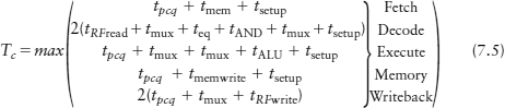
Example 7.10 PROCESSOR PERFORMANCE COMPARISON
Ben Bitdiddle needs to compare the pipelined processor performance to that of the single-cycle and multicycle processors considered in Example 7.8. Most of the logic delays were given in Table 7.6. The other element delays are 40 ps for an equality comparator, 15 ps for an AND gate, 100 ps for a register file write, and 220 ps for a memory write. Help Ben compare the execution time of 100 billion instructions from the SPECINT2000 benchmark for each processor.
Solution: According to Equation 7.5, the cycle time of the pipelined processor is Tc3 = max[30 + 250 + 20, 2(150 + 25 + 40 + 15 + 25 + 20), 30 + 25 + 25 + 200 + 20, 30 + 220 + 20, 2(30 + 25 + 100)] = 550 ps. According to Equation 7.1, the total execution time is T3 = (100 X 109 instructions)(1.15 cycles/ instruction)(550 X 10-12 s/cycle) = 63.3 seconds. This compares to 95 seconds for the single-cycle processor and 133.9 seconds for the multicycle processor.
The pipelined processor is substantially faster than the others. However, its advantage over the single-cycle processor is nowhere near the five-fold speedup one might hope to get from a five-stage pipeline. The pipeline hazards introduce a small CPI penalty. More significantly, the sequencing overhead (clk-to-Q and setup times) of the registers applies to every pipeline stage, not just once to the overall datapath. Sequencing overhead limits the benefits one can hope to achieve from pipelining.
The careful reader might observe that the Decode stage is substantially slower than the others, because the register file write, read, and branch comparison must all happen in half a cycle. Perhaps moving the branch comparison to the Decode stage was not such a good idea. If branches were resolved in the Execute stage instead, the CPI would increase slightly, because a mispredict would flush two instructions, but the cycle time would decrease substantially, giving an overall speedup.
The pipelined processor is similar in hardware requirements to the single-cycle processor, but it adds a substantial number of pipeline registers, along with multiplexers and control logic to resolve hazards.
7.6 HDL REPRESENTATION*
This section presents HDL code for the single-cycle MIPS processor supporting all of the instructions discussed in this chapter, including addi and j. The code illustrates good coding practices for a moderately complex system. HDL code for the multicycle processor and pipelined processor are left to Exercises 7.22 and 7.33.
In this section, the instruction and data memories are separated from the main processor and connected by address and data busses. This is more realistic, because most real processors have external memory. It also illustrates how the processor can communicate with the outside world.
The processor is composed of a datapath and a controller. The controller, in turn, is composed of the main decoder and the ALU decoder. Figure 7.59 shows a block diagram of the single-cycle MIPS processor interfaced to external memories.

Figure 7.59 MIPS single-cycle processor interfaced to external memory
The HDL code is partitioned into several sections. Section 7.6.1 provides HDL for the single-cycle processor datapath and controller. Section 7.6.2 presents the generic building blocks, such as registers and multiplexers, that are used by any microarchitecture. Section 7.6.3 introduces the testbench and external memories. The HDL is available in electronic form on the this book’s Web site (see the preface).
7.6.1 Single-Cycle Processor
The main modules of the single-cycle MIPS processor module are given in the following HDL examples.
HDL Example 7.1 SINGLE-CYCLE MIPS PROCESSOR
Verilog

VHDL

HDL Example 7.2 CONTROLLER
Verilog

VHDL

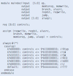

HDL Example 7.4 ALU DECODER
Verilog
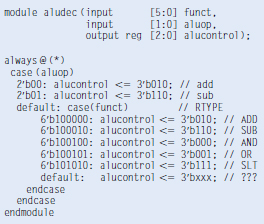
VHDL
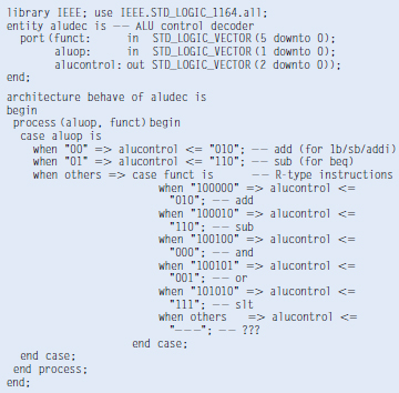

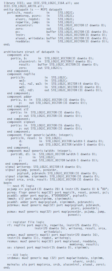
7.6.2 Generic Building Blocks
This section contains generic building blocks that may be useful in any MIPS microarchitecture, including a register file, adder, left shift unit, sign-extension unit, resettable flip-flop, and multiplexer. The HDL for the ALU is left to Exercise 5.9.
HDL Example 7.6 REGISTER FILE
Verilog
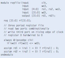
VHDL

HDL Example 7.7 ADDER
Verilog

VHDL

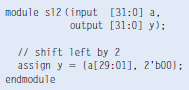

HDL Example 7.9 SIGN EXTENSION
Verilog
VHDL

HDL Example 7.10 RESETTABLE FLIP-FLOP
Verilog

VHDL


7.6.3 Testbench
The MIPS testbench loads a program into the memories. The program in Figure 7.60 exercises all of the instructions by performing a computation that should produce the correct answer only if all of the instructions are functioning properly. Specifically, the program will write the value 7 to address 84 if it runs correctly, and is unlikely to do so if the hardware is buggy. This is an example of ad hoc testing.

Figure 7.60 Assembly and machine code for MIPS test program
The machine code is stored in a hexadecimal file called memfile.dat (see Figure 7.61), which is loaded by the testbench during simulation. The file consists of the machine code for the instructions, one instruction per line.
Figure 7.61 Contents of memfile.dat
The testbench, top-level MIPS module, and external memory HDL code are given in the following examples. The memories in this example hold 64 words each.
HDL Example 7.12 MIPS TESTBENCH
Verilog
VHDL


HDL Example 7.14 MIPS DATA MEMORY


7.7 EXCEPTIONS*
Section 6.7.2 introduced exceptions, which cause unplanned changes in the flow of a program. In this section, we enhance the multicycle processor to support two types of exceptions: undefined instructions and arithmetic overflow. Supporting exceptions in other microarchitectures follows similar principles.
As described in Section 6.7.2, when an exception takes place, the processor copies the PC to the EPC register and stores a code in the Cause register indicating the source of the exception. Exception causes include 0x28 for undefined instructions and 0x30 for overflow (see Table 6.7). The processor then jumps to the exception handler at memory address 0x80000180. The exception handler is code that responds to the exception. It is part of the operating system.
Also as discussed in Section 6.7.2, the exception registers are part of Coprocessor 0, a portion of the MIPS processor that is used for system functions. Coprocessor 0 defines up to 32 special-purpose registers, including Cause and EPC. The exception handler may use the mfc0 (move from coprocessor 0) instruction to copy these special-purpose registers into a general-purpose register in the register file; the Cause register is Coprocessor 0 register 13, and EPC is register 14.
To handle exceptions, we must add EPC and Cause registers to the datapath and extend the PCSrc multiplexer to accept the exception handler address, as shown in Figure 7.62. The two new registers have write enables, EPCWrite and CauseWrite, to store the PC and exception cause when an exception takes place. The cause is generated by a multiplexer that selects the appropriate code for the exception. The ALU must also generate an overflow signal, as was discussed in Section 5.2.4.5
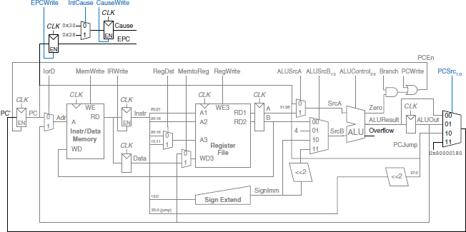
Figure 7.62 Datapath supporting overflow and undefined instruction exceptions
To support the mfc0 instruction, we also add a way to select the Coprocessor 0 registers and write them to the register file, as shown in Figure 7.63. The mfc0 instruction specifies the Coprocessor 0 register by Instr15:11; in this diagram, only the Cause and EPC registers are supported. We add another input to the MemtoReg multiplexer to select the value from Coprocessor 0.

Figure 7.63 Datapath supporting mfc0
The modified controller is shown in Figure 7.64. The controller receives the overflow flag from the ALU. It generates three new control signals: one to write the EPC, a second to write the Cause register, and a third to select the Cause. It also includes two new states to support the two exceptions and another state to handle mfc0.

Figure 7.64 Controller supporting exceptions and mfc0
If the controller receives an undefined instruction (one that it does not know how to handle), it proceeds to S12, saves the PC in EPC, writes 0x28 to the Cause register, and jumps to the exception handler. Similarly, if the controller detects arithmetic overflow on an add or sub instruction, it proceeds to S13, saves the PC in EPC, writes 0x30 in the Cause register, and jumps to the exception handler. Note that, when an exception occurs, the instruction is discarded and the register file is not written. When a mfc0 instruction is decoded, the processor goes to S14 and writes the appropriate Coprocessor 0 register to the main register file.
7.8 ADVANCED MICROARCHITECTURE*
High-performance microprocessors use a wide variety of techniques to run programs faster. Recall that the time required to run a program is proportional to the period of the clock and to the number of clock cycles per instruction (CPI). Thus, to increase performance we would like to speed up the clock and/or reduce the CPI. This section surveys some existing speedup techniques. The implementation details become quite complex, so we will focus on the concepts. Hennessy & Patterson’s Computer Architecture text is a definitive reference if you want to fully understand the details.
Every 2 to 3 years, advances in CMOS manufacturing reduce transistor dimensions by 30% in each direction, doubling the number of transistors that can fit on a chip. A manufacturing process is characterized by its feature size, which indicates the smallest transistor that can be reliably built. Smaller transistors are faster and generally consume less power. Thus, even if the microarchitecture does not change, the clock frequency can increase because all the gates are faster. Moreover, smaller transistors enable placing more transistors on a chip. Microarchitects use the additional transistors to build more complicated processors or to put more processors on a chip. Unfortunately, power consumption increases with the number of transistors and the speed at which they operate (see Section 1.8). Power consumption is now an essential concern. Microprocessor designers have a challenging task juggling the trade-offs among speed, power, and cost for chips with billions of transistors in some of the most complex systems that humans have ever built.
7.8.1 Deep Pipelines
Aside from advances in manufacturing, the easiest way to speed up the clock is to chop the pipeline into more stages. Each stage contains less logic, so it can run faster. This chapter has considered a classic five-stage pipeline, but 10 to 20 stages are now commonly used.
The maximum number of pipeline stages is limited by pipeline hazards, sequencing overhead, and cost. Longer pipelines introduce more dependencies. Some of the dependencies can be solved by forwarding, but others require stalls, which increase the CPI. The pipeline registers between each stage have sequencing overhead from their setup time and clk-to-Q delay (as well as clock skew). This sequencing overhead makes adding more pipeline stages give diminishing returns. Finally, adding more stages increases the cost because of the extra pipeline registers and hardware required to handle hazards.
Consider building a pipelined processor by chopping up the single-cycle processor into N stages (N ![]() 5). The single-cycle processor has a propagation delay of 900 ps through the combinational logic. The sequencing overhead of a register is 50 ps. Assume that the combinational delay can be arbitrarily divided into any number of stages and that pipeline hazard logic does not increase the delay. The five-stage pipeline in Example 7.9 has a CPI of 1.15. Assume that each additional stage increases the CPI by 0.1 because of branch mispredictions and other pipeline hazards. How many pipeline stages should be used to make the processor execute programs as fast as possible?
5). The single-cycle processor has a propagation delay of 900 ps through the combinational logic. The sequencing overhead of a register is 50 ps. Assume that the combinational delay can be arbitrarily divided into any number of stages and that pipeline hazard logic does not increase the delay. The five-stage pipeline in Example 7.9 has a CPI of 1.15. Assume that each additional stage increases the CPI by 0.1 because of branch mispredictions and other pipeline hazards. How many pipeline stages should be used to make the processor execute programs as fast as possible?
Solution: If the 900-ps combinational logic delay is divided into N stages and each stage also pays 50 ps of sequencing overhead for its pipeline register, the cycle time is Tc = 900/N + 50. The CPI is 1.15 + 0.1(N − 5). The time per instruction, or instruction time, is the product of the cycle time and the CPI. Figure 7.65 plots the cycle time and instruction time versus the number of stages. The instruction time has a minimum of 231 ps at N = 11 stages. This minimum is only slightly better than the 250 ps per instruction achieved with a six-stage pipeline.

Figure 7.65 Cycle time and instruction time versus the number of pipeline stages
In the late 1990s and early 2000s, microprocessors were marketed largely based on clock frequency (1/Tc). This pushed microprocessors to use very deep pipelines (20 to 31 stages on the Pentium 4) to maximize the clock frequency, even if the benefits for overall performance were questionable. Power is proportional to clock frequency and also increases with the number of pipeline registers, so now that power consumption is so important, pipeline depths are decreasing.
7.8.2 Branch Prediction
An ideal pipelined processor would have a CPI of 1. The branch misprediction penalty is a major reason for increased CPI. As pipelines get deeper, branches are resolved later in the pipeline. Thus, the branch misprediction penalty gets larger, because all the instructions issued after the mispredicted branch must be flushed. To address this problem, most pipelined processors use a branch predictor to guess whether the branch should be taken. Recall that our pipeline from Section 7.5.3 simply predicted that branches are never taken.
Some branches occur when a program reaches the end of a loop (e.g., a for or while statement) and branches back to repeat the loop. Loops tend to be executed many times, so these backward branches are usually taken. The simplest form of branch prediction checks the direction of the branch and predicts that backward branches should be taken. This is called static branch prediction, because it does not depend on the history of the program.
Forward branches are difficult to predict without knowing more about the specific program. Therefore, most processors use dynamic branch predictors, which use the history of program execution to guess whether a branch should be taken. Dynamic branch predictors maintain a table of the last several hundred (or thousand) branch instructions that the processor has executed. The table, sometimes called a branch target buffer, includes the destination of the branch and a history of whether the branch was taken.
To see the operation of dynamic branch predictors, consider the following loop code from Code Example 6.20. The loop repeats 10 times, and the beq out of the loop is taken only on the last time.
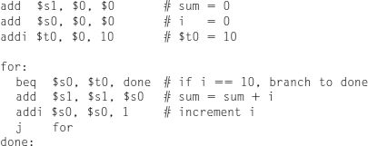
A one-bit dynamic branch predictor remembers whether the branch was taken the last time and predicts that it will do the same thing the next time. While the loop is repeating, it remembers that the beq was not taken last time and predicts that it should not be taken next time. This is a correct prediction until the last branch of the loop, when the branch does get taken. Unfortunately, if the loop is run again, the branch predictor remembers that the last branch was taken. Therefore, it incorrectly predicts that the branch should be taken when the loop is first run again. In summary, a 1-bit branch predictor mispredicts the first and last branches of a loop.
A 2-bit dynamic branch predictor solves this problem by having four states: strongly taken, weakly taken, weakly not taken, and strongly not taken, as shown in Figure 7.66. When the loop is repeating, it enters the “strongly not taken” state and predicts that the branch should not be taken next time. This is correct until the last branch of the loop, which is taken and moves the predictor to the “weakly not taken” state. When the loop is first run again, the branch predictor correctly predicts that the branch should not be taken and reenters the “strongly not taken” state. In summary, a 2-bit branch predictor mispredicts only the last branch of a loop.

Figure 7.66 2-bit branch predictor state transition diagram
As one can imagine, branch predictors may be used to track even more history of the program to increase the accuracy of predictions. Good branch predictors achieve better than 90% accuracy on typical programs.
The branch predictor operates in the Fetch stage of the pipeline so that it can determine which instruction to execute on the next cycle. When it predicts that the branch should be taken, the processor fetches the next instruction from the branch destination stored in the branch target buffer. By keeping track of both branch and jump destinations in the branch target buffer, the processor can also avoid flushing the pipeline during jump instructions.
A scalar processor acts on one piece of data at a time. A vector processor acts on several pieces of data with a single instruction. A superscalar processor issues several instructions at a time, each of which operates on one piece of data.
Our MIPS pipelined processor is a scalar processor. Vector processors were popular for supercomputers in the 1980s and 1990s because they efficiently handled the long vectors of data common in scientific computations. Modern high-performance microprocessors are superscalar, because issuing several independent instructions is more flexible than processing vectors.
However, modern processors also include hardware to handle short vectors of data that are common in multimedia and graphics applications. These are called single instruction multiple data (SIMD) units.
7.8.3 Superscalar Processor
A superscalar processor contains multiple copies of the datapath hardware to execute multiple instructions simultaneously. Figure 7.67 shows a block diagram of a two-way superscalar processor that fetches and executes two instructions per cycle. The datapath fetches two instructions at a time from the instruction memory. It has a six-ported register file to read four source operands and write two results back in each cycle. It also contains two ALUs and a two-ported data memory to execute the two instructions at the same time.

Figure 7.67 Superscalar datapath
Figure 7.68 shows a pipeline diagram illustrating the two-way superscalar processor executing two instructions on each cycle. For this program, the processor has a CPI of 0.5. Designers commonly refer to the reciprocal of the CPI as the instructions per cycle, or IPC. This processor has an IPC of 2 on this program.

Figure 7.68 Abstract view of a superscalar pipeline in operation
Executing many instructions simultaneously is difficult because of dependencies. For example, Figure 7.69 shows a pipeline diagram running a program with data dependencies. The dependencies in the code are shown in blue. The add instruction is dependent on $t0, which is produced by the lw instruction, so it cannot be issued at the same time as lw. Indeed, the add instruction stalls for yet another cycle so that lw can forward $t0 to add in cycle 5. The other dependencies (between sub and and based on $t0, and between or and sw based on $t3) are handled by forwarding results produced in one cycle to be consumed in the next. This program, also given below, requires five cycles to issue six instructions, for an IPC of 1.17.

Figure 7.69 Program with data dependencies

Recall that parallelism comes in temporal and spatial forms. Pipelining is a case of temporal parallelism. Multiple execution units is a case of spatial parallelism. Superscalar processors exploit both forms of parallelism to squeeze out performance far exceeding that of our single-cycle and multicycle processors.
Commercial processors may be three-, four-, or even six-way superscalar. They must handle control hazards such as branches as well as data hazards. Unfortunately, real programs have many dependencies, so wide superscalar processors rarely fully utilize all of the execution units. Moreover, the large number of execution units and complex forwarding networks consume vast amounts of circuitry and power.
7.8.4 Out-of-Order Processor
To cope with the problem of dependencies, an out-of-order processor looks ahead across many instructions to issue, or begin executing, independent instructions as rapidly as possible. The instructions can be issued in a different order than that written by the programmer, as long as dependencies are honored so that the program produces the intended result.
Consider running the same program from Figure 7.69 on a two-way superscalar out-of-order processor. The processor can issue up to two instructions per cycle from anywhere in the program, as long as dependencies are observed. Figure 7.70 shows the data dependencies and the operation of the processor. The classifications of dependencies as RAW and WAR will be discussed shortly. The constraints on issuing instructions are described below.

Figure 7.70 Out-of-order execution of a program with dependencies
lw instruction issues.add, sub, and and instructions are dependent on lw by way of $t0, so they cannot issue yet. However, the or instruction is independent, so it also issues.lw instruction issues and when a dependent instruction can use its result, so add cannot issue yet because of the $t0 dependence. sub writes $t0, so it cannot issue before add, lest add receive the wrong value of $t0. and is dependent on sub.sw instruction issues.$t0 is available, so add issues. sub issues simultaneously, because it will not write $t0 until after add consumes $t0.and instruction issues. $t0 is forwarded from sub to and.The out-of-order processor issues the six instructions in four cycles, for an IPC of 1.5.
The dependence of add on lw by way of $t0 is a read after write (RAW) hazard. add must not read $t0 until after lw has written it. This is the type of dependency we are accustomed to handling in the pipelined processor. It inherently limits the speed at which the program can run, even if infinitely many execution units are available. Similarly, the dependence of sw on or by way of $t3 and of and on sub by way of $t0 are RAW dependencies.
The dependence between sub and add by way of $t0 is called a write after read (WAR) hazard or an antidependence. sub must not write $t0 before add reads $t0, so that add receives the correct value according to the original order of the program. WAR hazards could not occur in the simple MIPS pipeline, but they may happen in an out-of-order processor if the dependent instruction (in this case, sub) is moved too early.
A WAR hazard is not essential to the operation of the program. It is merely an artifact of the programmer’s choice to use the same register for two unrelated instructions. If the sub instruction had written $t4 instead of $t0, the dependency would disappear and sub could be issued before add. The MIPS architecture only has 32 registers, so sometimes the programmer is forced to reuse a register and introduce a hazard just because all the other registers are in use.
A third type of hazard, not shown in the program, is called write after write (WAW) or an output dependence. A WAW hazard occurs if an instruction attempts to write a register after a subsequent instruction has already written it. The hazard would result in the wrong value being written to the register. For example, in the following program, add and sub both write $t0. The final value in $t0 should come from sub according to the order of the program. If an out-of-order processor attempted to execute sub first, the WAW hazard would occur.
add $t0, $s1, $s2
sub $t0, $s3, $s4
WAW hazards are not essential either; again, they are artifacts caused by the programmer’s using the same register for two unrelated instructions. If the sub instruction were issued first, the program could eliminate the WAW hazard by discarding the result of the add instead of writing it to $t0. This is called squashing the add.6
Out-of-order processors use a table to keep track of instructions waiting to issue. The table, sometimes called a scoreboard, contains information about the dependencies. The size of the table determines how many instructions can be considered for issue. On each cycle, the processor examines the table and issues as many instructions as it can, limited by the dependencies and by the number of execution units (e.g., ALUs, memory ports) that are available.
The instruction level parallelism (ILP) is the number of instructions that can be executed simultaneously for a particular program and microarchitecture. Theoretical studies have shown that the ILP can be quite large for out-of-order microarchitectures with perfect branch predictors and enormous numbers of execution units. However, practical processors seldom achieve an ILP greater than 2 or 3, even with six-way superscalar datapaths with out-of-order execution.
7.8.5 Register Renaming
Out-of-order processors use a technique called register renaming to eliminate WAR hazards. Register renaming adds some nonarchitectural renaming registers to the processor. For example, a MIPS processor might add 20 renaming registers, called $r0-$r19. The programmer cannot use these registers directly, because they are not part of the architecture. However, the processor is free to use them to eliminate hazards.
For example, in the previous section, a WAR hazard occurred between the sub and add instructions based on reusing $t0. The out-of-order processor could rename $t0 to $r0 for the sub instruction. Then sub could be executed sooner, because $r0 has no dependency on the add instruction. The processor keeps a table of which registers were renamed so that it can consistently rename registers in subsequent dependent instructions. In this example, $t0 must also be renamed to $r0 in the and instruction, because it refers to the result of sub.
Figure 7.71 shows the same program from Figure 7.70 executing on an out-of-order processor with register renaming. $t0 is renamed to $r0 in sub and and to eliminate the WAR hazard. The constraints on issuing instructions are described below.

Figure 7.71 Out-of-order execution of a program using register renaming
lw instruction issues.add instruction is dependent on lw by way of $t0, so it cannot issue yet. However, the sub instruction is independent now that its destination has been renamed to $r0, so sub also issues.lw issues and when a dependent instruction can use its result, so add cannot issue yet because of the $t0 dependence.and instruction is dependent on sub, so it can issue. $r0 is forwarded from sub to and.or instruction is independent, so it also issues.$t0 is available, so add issues. $t3 is also available, so sw issues.The out-of-order processor with register renaming issues the six instructions in three cycles, for an IPC of 2.
7.8.6 Single Instruction Multiple Data
The term SIMD (pronounced “sim-dee”) stands for single instruction multiple data, in which a single instruction acts on multiple pieces of data in parallel. A common application of SIMD is to perform many short arithmetic operations at once, especially for graphics processing. This is also called packed arithmetic.
For example, a 32-bit microprocessor might pack four 8-bit data elements into one 32-bit word. Packed add and subtract instructions operate on all four data elements within the word in parallel. Figure 7.72 shows a packed 8-bit addition summing four pairs of 8-bit numbers to produce four results. The word could also be divided into two 16-bit elements. Performing packed arithmetic requires modifying the ALU to eliminate carries between the smaller data elements. For example, a carry out of a0 + b0 should not affect the result of a1 + b1.
Figure 7.72 Packed arithmetic: four simultaneous 8-bit additions
Short data elements often appear in graphics processing. For example, a pixel in a digital photo may use 8 bits to store each of the red, green, and blue color components. Using an entire 32-bit word to process one of these components wastes the upper 24 bits. When the components from four adjacent pixels are packed into a 32-bit word, the processing can be performed four times faster.
SIMD instructions are even more helpful for 64-bit architectures, which can pack eight 8-bit elements, four 16-bit elements, or two 32-bit elements into a single 64-bit word. SIMD instructions are also used for floating-point computations; for example, four 32-bit single-precision floating-point values can be packed into a single 128-bit word.
7.8.7 Multithreading
Because the ILP of real programs tends to be fairly low, adding more execution units to a superscalar or out-of-order processor gives diminishing returns. Another problem, discussed in Chapter 8, is that memory is much slower than the processor. Most loads and stores access a smaller and faster memory, called a cache. However, when the instructions or data are not available in the cache, the processor may stall for 100 or more cycles while retrieving the information from the main memory. Multithreading is a technique that helps keep a processor with many execution units busy even if the ILP of a program is low or the program is stalled waiting for memory.
To explain multithreading, we need to define a few new terms. A program running on a computer is called a process. Computers can run multiple processes simultaneously; for example, you can play music on a PC while surfing the web and running a virus checker. Each process consists of one or more threads that also run simultaneously. For example, a word processor may have one thread handling the user typing, a second thread spell-checking the document while the user works, and a third thread printing the document. In this way, the user does not have to wait, for example, for a document to finish printing before being able to type again.
In a conventional processor, the threads only give the illusion of running simultaneously. The threads actually take turns being executed on the processor under control of the OS. When one thread’s turn ends, the OS saves its architectural state, loads the architectural state of the next thread, and starts executing that next thread. This procedure is called context switching. As long as the processor switches through all the threads fast enough, the user perceives all of the threads as running at the same time.
A multithreaded processor contains more than one copy of its architectural state, so that more than one thread can be active at a time. For example, if we extended a MIPS processor to have four program counters and 128 registers, four threads could be available at one time. If one thread stalls while waiting for data from main memory, the processor could context switch to another thread without any delay, because the program counter and registers are already available. Moreover, if one thread lacks sufficient parallelism to keep all the execution units busy, another thread could issue instructions to the idle units.
Multithreading does not improve the performance of an individual thread, because it does not increase the ILP. However, it does improve the overall throughput of the processor, because multiple threads can use processor resources that would have been idle when executing a single thread. Multithreading is also relatively inexpensive to implement, because it replicates only the PC and register file, not the execution units and memories.
7.8.8 Multiprocessors
A multiprocessor system consists of multiple processors and a method for communication between the processors. A common form of multiprocessing in computer systems is symmetric multiprocessing (SMP), in which two or more identical processors share a single main memory.
The multiple processors may be separate chips or multiple cores on the same chip. Modern processors have enormous numbers of transistors available. Using them to increase the pipeline depth or to add more execution units to a superscalar processor gives little performance benefit and is wasteful of power. Around the year 2005, computer architects made a major shift to build multiple copies of the processor on the same chip; these copies are called cores.
Scientists searching for signs of extraterrestrial intelligence use the world’s largest clustered multiprocessors to analyze radio telescope data for patterns that might be signs of life in other solar systems. The cluster consists of personal computers owned by more than 3.8 million volunteers around the world.
When a computer in the cluster is idle, it fetches a piece of the data from a centralized server, analyzes the data, and sends the results back to the server. You can volunteer your computer’s idle time for the cluster by visiting setiathome.berkeley.edu.
Multiprocessors can be used to run more threads simultaneously or to run a particular thread faster. Running more threads simultaneously is easy; the threads are simply divided up among the processors. Unfortunately typical PC users need to run only a small number of threads at any given time. Running a particular thread faster is much more challenging. The programmer must divide the thread into pieces to perform on each processor. This becomes tricky when the processors need to communicate with each other. One of the major challenges for computer designers and programmers is to effectively use large numbers of processor cores.
Other forms of multiprocessing include asymmetric multiprocessing and clusters. Asymmetric multiprocessors use separate specialized microprocessors for separate tasks. For example, a cell phone contains a digital signal processor (DSP) with specialized instructions to decipher the wireless data in real time and a separate conventional processor to interact with the user, manage the phone book, and play games. In clustered multiprocessing, each processor has its own local memory system. Clustering can also refer to a group of PCs connected together on the network running software to jointly solve a large problem.
7.9 REAL-WORLD PERSPECTIVE: IA-32 MICROARCHITECTURE*
Section 6.8 introduced the IA-32 architecture used in almost all PCs. This section tracks the evolution of IA-32 processors through progressively faster and more complicated microarchitectures. The same principles we have applied to the MIPS microarchitectures are used in IA-32.
Intel invented the first single-chip microprocessor, the 4-bit 4004, in 1971 as a flexible controller for a line of calculators. It contained 2300 transistors manufactured on a 12-mm2 sliver of silicon in a process with a 10-μm feature size and operated at 750 KHz. A photograph of the chip taken under a microscope is shown in Figure 7.73. In places, columns of four similar-looking structures are visible, as one would expect in a 4-bit microprocessor. Around the periphery are bond wires, which are used to connect the chip to its package and the circuit board.

Figure 7.73 4004 microprocessor chip
The 4004 inspired the 8-bit 8008, then the 8080, which eventually evolved into the 16-bit 8086 in 1978 and the 80286 in 1982. In 1985, Intel introduced the 80386, which extended the 8086 architecture to 32 bits and defined the IA-32 architecture. Table 7.7 summarizes major Intel IA-32 microprocessors. In the 35 years since the 4004, transistor feature size has shrunk 160-fold, the number of transistors on a chip has increased by five orders of magnitude, and the operating frequency has increased by almost four orders of magnitude. No other field of engineering has made such astonishing progress in such a short time.
Table 7.7 Evolution of Intel IA-32 microprocessors

The 80386 is a multicycle processor. The major components are labeled on the chip photograph in Figure 7.74. The 32-bit datapath is clearly visible on the left. Each of the columns processes one bit of data. Some of the control signals are generated using a microcode PLA that steps through the various states of the control FSM. The memory management unit in the upper right controls access to the external memory.

Figure 7.74 80386 microprocessor chip
The 80486, shown in Figure 7.75, dramatically improved performance using pipelining. The datapath is again clearly visible, along with the control logic and microcode PLA. The 80486 added an on-chip floating-point unit; previous Intel processors either sent floating-point instructions to a separate coprocessor or emulated them in software. The 80486 was too fast for external memory to keep up, so it incorporated an 8-KB cache onto the chip to hold the most commonly used instructions and data. Chapter 8 describes caches in more detail and revisits the cache systems on Intel IA-32 processors.
Figure 7.75 80486 microprocessor chip
The Pentium processor, shown in Figure 7.76, is a superscalar processor capable of executing two instructions simultaneously. Intel switched to the name Pentium instead of 80586 because AMD was becoming a serious competitor selling interchangeable 80486 chips, and part numbers cannot be trademarked. The Pentium uses separate instruction and data caches. It also uses a branch predictor to reduce the performance penalty for branches.

Figure 7.76 Pentium microprocessor chip
The Pentium Pro, Pentium II, and Pentium III processors all share a common out-of-order microarchitecture, code named P6. The complex IA-32 instructions are broken down into one or more micro-ops similar to MIPS instructions. The micro-ops are then executed on a fast out-of-order execution core with an 11-stage pipeline. Figure 7.77 shows the Pentium III. The 32-bit datapath is called the Integer Execution Unit (IEU). The floating-point datapath is called the Floating Point Unit (FPU). The processor also has a SIMD unit to perform packed operations on short integer and floating-point data. A larger portion of the chip is dedicated to issuing instructions out-of-order than to actually executing the instructions. The instruction and data caches have grown to 16 KB each. The Pentium III also has a larger but slower 256-KB second-level cache on the same chip.
Figure 7.77 Pentium III microprocessor chip
By the late 1990s, processors were marketed largely on clock speed. The Pentium 4 is another out-of-order processor with a very deep pipeline to achieve extremely high clock frequencies. It started with 20 stages, and later versions adopted 31 stages to achieve frequencies greater than 3 GHz. The chip, shown in Figure 7.78, packs in 42 to 178 million transistors (depending on the cache size), so even the major execution units are difficult to see on the photograph. Decoding three IA-32 instructions per cycle is impossible at such high clock frequencies because the instruction encodings are so complex and irregular. Instead, the processor predecodes the instructions into simpler micro-ops, then stores the micro-ops in a memory called a trace cache. Later versions of the Pentium 4 also perform multithreading to increase the throughput of multiple threads.

Figure 7.78 Pentium 4 microprocessor chip
The Pentium 4’s reliance on deep pipelines and high clock speed led to extremely high power consumption, sometimes more than 100 W. This is unacceptable in laptops and makes cooling of desktops expensive. Intel discovered that the older P6 architecture could achieve comparable performance at much lower clock speed and power. The Pentium M uses an enhanced version of the P6 out-of-order microarchitecture with 32-KB instruction and data caches and a 1- to 2-MB second-level cache. The Core Duo is a multicore processor based on two Pentium M cores connected to a shared 2-MB second-level cache. The individual functional units in Figure 7.79 are difficult to see, but the two cores and the large cache are clearly visible.
Figure 7.79 Core Duo microprocessor chip
7.10 SUMMARY
This chapter has described three ways to build MIPS processors, each with different performance and cost trade-offs. We find this topic almost magical: how can such a seemingly complicated device as a microprocessor actually be simple enough to fit in a half-page schematic? Moreover, the inner workings, so mysterious to the uninitiated, are actually reasonably straightforward.
The MIPS microarchitectures have drawn together almost every topic covered in the text so far. Piecing together the microarchitecture puzzle illustrates the principles introduced in previous chapters including the design of combinational and sequential circuits, covered in Chapters 2 and 3; the application of many of the building blocks described in Chapter 5; and the implementation of the MIPS architecture introduced in Chapter 6. The MIPS microarchitectures can be described in a few pages of HDL, using the techniques from Chapter 4.
Building the microarchitectures has also heavily used our techniques for managing complexity. The microarchitectural abstraction forms the link between the logic and architecture abstractions forming the crux of this book on digital design and computer architecture. We also use the abstractions of block diagrams and HDL to succinctly describe the arrangement of components. The microarchitectures exploit regularity and modularity, reusing a library of common building blocks such as ALUs, memories, multiplexers, and registers. Hierarchy is used in numerous ways. The microarchitectures are partitioned into the datapath and control units. Each of these units is built from logic blocks, which can be built from gates, which in turn can be built from transistors using the techniques developed in the first five chapters.
This chapter has compared single-cycle, multicycle, and pipelined microarchitectures for the MIPS processor. All three microarchitectures implement the same subset of the MIPS instruction set and have the same architectural state. The single-cycle processor is the most straightforward and has a CPI of 1.
The multicycle processor uses a variable number of shorter steps to execute instructions. It thus can reuse the ALU, rather than requiring several adders. However, it does require several nonarchitectural registers to store results between steps. The multicycle design in principle could be faster, because not all instructions must be equally long. In practice, it is generally slower, because it is limited by the slowest steps and by the sequencing overhead in each step.
The pipelined processor divides the single-cycle processor into five relatively fast pipeline stages. It adds pipeline registers between the stages to separate the five instructions that are simultaneously executing. It nominally has a CPI of 1, but hazards force stalls or flushes that increase the CPI slightly. Hazard resolution also costs some extra hardware and design complexity. The clock period ideally could be five times shorter than that of the single-cycle processor. In practice, it is not that short, because it is limited by the slowest stage and by the sequencing overhead in each stage. Nevertheless, pipelining provides substantial performance benefits. All modern high-performance microprocessors use pipelining today.
Although the microarchitectures in this chapter implement only a subset of the MIPS architecture, we have seen that supporting more instructions involves straightforward enhancements of the datapath and controller. Supporting exceptions also requires simple modifications.
A major limitation of this chapter is that we have assumed an ideal memory system that is fast and large enough to store the entire program and data. In reality, large fast memories are prohibitively expensive. The next chapter shows how to get most of the benefits of a large fast memory with a small fast memory that holds the most commonly used information and one or more larger but slower memories that hold the rest of the information.
Exercises
Exercise 7.1 Suppose that one of the following control signals in the single-cycle MIPS processor has a stuck-at-0 fault, meaning that the signal is always 0, regardless of its intended value. What instructions would malfunction? Why?
Exercise 7.2 Repeat Exercise 7.1, assuming that the signal has a stuck-at-1 fault.
Exercise 7.3 Modify the single-cycle MIPS processor to implement one of the following instructions. See Appendix B for a definition of the instructions. Mark up a copy of Figure 7.11 to indicate the changes to the datapath. Name any new control signals. Mark up a copy of Table 7.8 to show the changes to the main decoder. Describe any other changes that are required.
Table 7.8 Main decoder truth table to mark up with changes
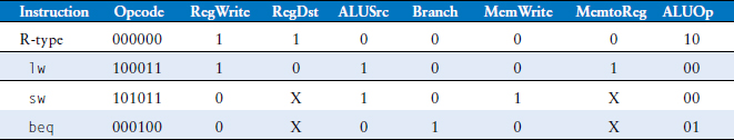
Exercise 7.4 Many processor architectures have a load with postincrement instruction, which updates the index register to point to the next memory word after completing the load. lwinc $rt, imm($rs) is equivalent to the following two instructions:
lw $rt, imm($rs)
addi $rs, $rs, 4
Repeat Exercise 7.3 for the lwinc instruction. Is it possible to add the instruction without modifying the register file?
Exercise 7.5 Add a single-precision floating-point unit to the single-cycle MIPS processor to handle add.s, sub.s, and mul.s. Assume that you have single-precision floating-point adder and multiplier units available. Explain what changes must be made to the datapath and the controller.
Exercise 7.6 Your friend is a crack circuit designer. She has offered to redesign one of the units in the single-cycle MIPS processor to have half the delay. Using the delays from Table 7.6, which unit should she work on to obtain the greatest speedup of the overall processor, and what would the cycle time of the improved machine be?
Exercise 7.7 Consider the delays given in Table 7.6. Ben Bitdiddle builds a prefix adder that reduces the ALU delay by 20 ps. If the other element delays stay the same, find the new cycle time of the single-cycle MIPS processor and determine how long it takes to execute a benchmark with 100 billion instructions.
Exercise 7.8 Suppose one of the following control signals in the multicycle MIPS processor has a stuck-at-0 fault, meaning that the signal is always 0, regardless of its intended value. What instructions would malfunction? Why?
Exercise 7.9 Repeat Exercise 7.8, assuming that the signal has a stuck-at-1 fault.
Exercise 7.10 Modify the HDL code for the single-cycle MIPS processor, given in Section 7.6.1, to handle one of the new instructions from Exercise 7.3. Enhance the testbench, given in Section 7.6.3 to test the new instruction.
Exercise 7.11 Modify the multicycle MIPS processor to implement one of the following instructions. See Appendix B for a definition of the instructions. Mark up a copy of Figure 7.27 to indicate the changes to the datapath. Name any new control signals. Mark up a copy of Figure 7.39 to show the changes to the controller FSM. Describe any other changes that are required.
Exercise 7.12 Repeat Exercise 7.4 for the multicycle MIPS processor. Show the changes to the multicycle datapath and control FSM. Is it possible to add the instruction without modifying the register file?
Exercise 7.13 Repeat Exercise 7.5 for the multicycle MIPS processor.
Exercise 7.14 Suppose that the floating-point adder and multiplier from Exercise 7.13 each take two cycles to operate. In other words, the inputs are applied at the beginning of one cycle, and the output is available in the second cycle. How does your answer to Exercise 7.13 change?
Exercise 7.15 Your friend, the crack circuit designer, has offered to redesign one of the units in the multicycle MIPS processor to be much faster. Using the delays from Table 7.6, which unit should she work on to obtain the greatest speedup of the overall processor? How fast should it be? (Making it faster than necessary is a waste of your friend’s effort.) What is the cycle time of the improved processor?
Exercise 7.16 Repeat Exercise 7.7 for the multicycle processor.
Exercise 7.17 Suppose the multicycle MIPS processor has the component delays given in Table 7.6. Alyssa P. Hacker designs a new register file that has 40% less power but twice as much delay. Should she switch to the slower but lower power register file for her multicycle processor design?
Exercise 7.18 Goliath Corp claims to have a patent on a three-ported register file. Rather than fighting Goliath in court, Ben Bitdiddle designs a new register file that has only a single read/write port (like the combined instruction and data memory). Redesign the MIPS multicycle datapath and controller to use his new register file.
Exercise 7.19 What is the CPI of the redesigned multicycle MIPS processor from Exercise 7.18? Use the instruction mix from Example 7.7.
Exercise 7.20 How many cycles are required to run the following program on the multicycle MIPS processor? What is the CPI of this program?
Exercise 7.21 Repeat Exercise 7.20 for the following program.

Exercise 7.22 Write HDL code for the multicycle MIPS processor. The processor should be compatible with the following top-level module. The mem module is used to hold both instructions and data. Test your processor using the testbench from Section 7.6.3.

Exercise 7.23 Extend your HDL code for the multicycle MIPS processor from Exercise 7.22 to handle one of the new instructions from Exercise 7.11. Enhance the testbench to test the new instruction.
Exercise 7.24 The pipelined MIPS processor is running the following program. Which registers are being written, and which are being read on the fifth cycle?
Exercise 7.25 Using a diagram similar to Figure 7.52, show the forwarding and stalls needed to execute the following instructions on the pipelined MIPS processor.

Exercise 7.26 Repeat Exercise 7.25 for the following instructions.
Exercise 7.27 How many cycles are required for the pipelined MIPS processor to issue all of the instructions for the program in Exercise 7.21? What is the CPI of the processor on this program?
Exercise 7.28 Explain how to extend the pipelined MIPS processor to handle the addi instruction.
Exercise 7.29 Explain how to extend the pipelined processor to handle the j instruction. Give particular attention to how the pipeline is flushed when a jump takes place.
Exercise 7.30 Examples 7.9 and 7.10 point out that the pipelined MIPS processor performance might be better if branches take place during the Execute stage rather than the Decode stage. Show how to modify the pipelined processor from Figure 7.58 to branch in the Execute stage. How do the stall and flush signals change? Redo Examples 7.9 and 7.10 to find the new CPI, cycle time, and overall time to execute the program.
Exercise 7.31 Your friend, the crack circuit designer, has offered to redesign one of the units in the pipelined MIPS processor to be much faster. Using the delays from Table 7.6 and Example 7.10, which unit should she work on to obtain the greatest speedup of the overall processor? How fast should it be? (Making it faster than necessary is a waste of your friend’s effort.) What is the cycle time of the improved processor?
Exercise 7.32 Consider the delays from Table 7.6 and Example 7.10. Now suppose that the ALU were 20% faster. Would the cycle time of the pipelined MIPS processor change? What if the ALU were 20% slower?
Exercise 7.33 Write HDL code for the pipelined MIPS processor. The processor should be compatible with the top-level module from HDL Example 7.13. It should support all of the instructions described in this chapter, including addi and j (see Exercises 7.28 and 7.29). Test your design using the testbench from HDL Example 7.12.
Exercise 7.34 Design the hazard unit shown in Figure 7.58 for the pipelined MIPS processor. Use an HDL to implement your design. Sketch the hardware that a synthesis tool might generate from your HDL.
Exercise 7.35 A nonmaskable interrupt (NMI) is triggered by an input pin to the processor. When the pin is asserted, the current instruction should finish, then the processor should set the Cause register to 0 and take an exception. Show how to modify the multicycle processor in Figures 7.63 and 7.64 to handle nonmaskable interrupts.
Interview Questions
The following exercises present questions that have been asked at interviews for digital design jobs.
Question 7.1 Explain the advantages of pipelined microprocessors.
Question 7.2 If additional pipeline stages allow a processor to go faster, why don’t processors have 100 pipeline stages?
Question 7.3 Describe what a hazard is in a microprocessor and explain ways in which it can be resolved. What are the pros and cons of each way?
Question 7.4 Describe the concept of a superscalar processor and its pros and cons.
1 This is an oversimplification used to treat the instruction memory as a ROM; in most real processors, the instruction memory must be writable so that the OS can load a new program into memory. The multicycle microarchitecture described in Section 7.4 is more realistic in that it uses a combined memory for instructions and data that can be both read and written.
2 Now we see why the PCSrc multiplexer is necessary to choose PC from either ALUResult (in S0) or ALUOut (in S8).
3 Data from Patterson and Hennessy, Computer Organization and Design, 3rd Edition, Morgan Kaufmann, 2005.
4 Strictly speaking, only the register designations (RsE, RtE, and RdE) and the control signals that might update memory or architectural state (RegWrite, MemWrite, and Branch) need to be cleared; as long as these signals are cleared, the bubble can contain random data that has no effect.
5 Strictly speaking, the ALU should assert overflow only for add and sub, not for other ALU instructions.
6 You might wonder why the add needs to be issued at all. The reason is that out-of-order processors must guarantee that all of the same exceptions occur that would have occurred if the program had been executed in its original order. The add potentially may produce an overflow exception, so it must be issued to check for the exception, even though the result can be discarded.