
Chapter 4 Hardware description languages
4.1 INTRODUCTION
Thus far, we have focused on designing combinational and sequential digital circuits at the schematic level. The process of finding an efficient set of logic gates to perform a given function is labor intensive and error prone, requiring manual simplification of truth tables or Boolean equations and manual translation of finite state machines (FSMs) into gates. In the 1990’s, designers discovered that they were far more productive if they worked at a higher level of abstraction, specifying just the logical function and allowing a computer-aided design (CAD) tool to produce the optimized gates. The specifications are generally given in a hardware description language (HDL). The two leading hardware description languages are Verilog and VHDL.
Verilog and VHDL are built on similar principles but have different syntax. Discussion of these languages in this chapter is divided into two columns for literal side-by-side comparison, with Verilog on the left and VHDL on the right. When you read the chapter for the first time, focus on one language or the other. Once you know one, you’ll quickly master the other if you need it.
Subsequent chapters show hardware in both schematic and HDL form. If you choose to skip this chapter and not learn one of the HDLs, you will still be able to master the principles of computer organization from the schematics. However, the vast majority of commercial systems are now built using HDLs rather than schematics. If you expect to do digital design at any point in your professional life, we urge you to learn one of the HDLs.
4.1.1 Modules
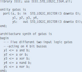
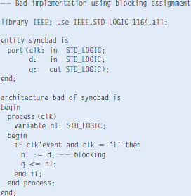
A block of hardware with inputs and outputs is called a module. An AND gate, a multiplexer, and a priority circuit are all examples of hardware modules. The two general styles for describing module functionality are behavioral and structural. Behavioral models describe what a module does. Structural models describe how a module is built from simpler pieces; it is an application of hierarchy. The Verilog and VHDL code in HDL Example 4.1 illustrate behavioral descriptions of a module that computes the Boolean function from Example 2.6, y = ![]() . In both languages, the module is named sillyfunction and has three inputs, a, b, and c, and one output, y.
. In both languages, the module is named sillyfunction and has three inputs, a, b, and c, and one output, y.
HDL Example 4.1 COMBINATIONAL LOGIC
Verilog

A Verilog module begins with the module name and a listing of the inputs and outputs. The assign statement describes combinational logic. ∼ indicates NOT, & indicates AND, and | indicates OR.
Verilog signals such as the inputs and outputs are Boolean variables (0 or 1). They may also have floating and undefined values, as discussed in Section 4.2.8.
VHDL
VHDL code has three parts: the library use clause, the entity declaration, and the architecture body. The library use clause is required and will be discussed in Section 4.2.11. The entity declaration lists the module name and its inputs and outputs. The architecture body defines what the module does.
VHDL signals, such as inputs and outputs, must have a type declaration. Digital signals should be declared to be STD_LOGIC type. STD_LOGIC signals can have a value of ‘0’ or ‘1’, as well as floating and undefined values that will be described in Section 4.2.8. The STD_LOGIC type is defined in the IEEE.STD_LOGIC_1164 library, which is why the library must be used.
VHDL lacks a good default order of operations, so Boolean equations should be parenthesized.
A module, as you might expect, is a good application of modularity. It has a well defined interface, consisting of its inputs and outputs, and it performs a specific function. The particular way in which it is coded is unimportant to others that might use the module, as long as it performs its function.
4.1.2 Language Origins
Universities are almost evenly split on which of these languages is taught in a first course, and industry is similarly split on which language is preferred. Compared to Verilog, VHDL is more verbose and cumbersome, as you might expect of a language developed by committee. U.S. military contractors, the European Space Agency, and telecommunications companies use VHDL extensively.
Verilog
Verilog was developed by Gateway Design Automation as a proprietary language for logic simulation in 1984. Gateway was acquired by Cadence in 1989 and Verilog was made an open standard in 1990 under the control of Open Verilog International. The language became an IEEE standard1 in 1995 (IEEE STD 1364) and was updated in 2001.
VHDL
VHDL is an acronym for the VHSIC Hardware Description Language. VHSIC is in turn an acronym for the Very High Speed Integrated Circuits program of the US Department of Defense.
VHDL was originally developed in 1981 by the Department of Defense to describe the structure and function of hardware. Its roots draw from the Ada programming language. The IEEE standardized it in 1987 (IEEE STD 1076) and has updated the standard several times since. The language was first envisioned for documentation but was quickly adopted for simulation and synthesis.
Both languages are fully capable of describing any hardware system, and both have their quirks. The best language to use is the one that is already being used at your site or the one that your customers demand. Most CAD tools today allow the two languages to be mixed, so that different modules can be described in different languages.
The term “bug” predates the invention of the computer. Thomas Edison called the “little faults and difficulties” with his inventions “bugs” in 1878.
The first real computer bug was a moth, which got caught between the relays of the Harvard Mark II electromechanical computer in 1947. It was found by Grace Hopper, who logged the incident, along with the moth itself and the comment “first actual case of bug being found.”

Source: Notebook entry courtesy Naval Historical Center, US Navy; photo No. NII 96566-KN
4.1.3 Simulation and Synthesis
The two major purposes of HDLs are logic simulation and synthesis. During simulation, inputs are applied to a module, and the outputs are checked to verify that the module operates correctly. During synthesis, the textual description of a module is transformed into logic gates.
Simulation
Humans routinely make mistakes. Such errors in hardware designs are called bugs. Eliminating the bugs from a digital system is obviously important, especially when customers are paying money and lives depend on the correct operation. Testing a system in the laboratory is time-consuming. Discovering the cause of errors in the lab can be extremely difficult, because only signals routed to the chip pins can be observed. There is no way to directly observe what is happening inside a chip. Correcting errors after the system is built can be devastatingly expensive. For example, correcting a mistake in a cutting-edge integrated circuit costs more than a million dollars and takes several months. Intel’s infamous FDIV (floating point division) bug in the Pentium processor forced the company to recall chips after they had shipped, at a total cost of $475 million. Logic simulation is essential to test a system before it is built.
Figure 4.1 shows waveforms from a simulation2 of the previous sillyfunction module demonstrating that the module works correctly. y is TRUE when a, b, and c are 000, 100, or 101, as specified by the Boolean equation.

Figure 4.1 Simulation waveforms
Synthesis
Logic synthesis transforms HDL code into a netlist describing the hardware (e.g., the logic gates and the wires connecting them). The logic synthesizer might perform optimizations to reduce the amount of hardware required. The netlist may be a text file, or it may be drawn as a schematic to help visualize the circuit. Figure 4.2 shows the results of synthesizing the sillyfunction module.3 Notice how the three three-input AND gates are simplified into two two-input AND gates, as we discovered in Example 2.6 using Boolean algebra.
Figure 4.2 Synthesized circuit
Circuit descriptions in HDL resemble code in a programming language. However, you must remember that the code is intended to represent hardware. Verilog and VHDL are rich languages with many commands. Not all of these commands can be synthesized into hardware. For example, a command to print results on the screen during simulation does not translate into hardware. Because our primary interest is to build hardware, we will emphasize a synthesizable subset of the languages. Specifically, we will divide HDL code into synthesizable modules and a testbench. The synthesizable modules describe the hardware. The testbench contains code to apply inputs to a module, check whether the output results are correct, and print discrepancies between expected and actual outputs. Testbench code is intended only for simulation and cannot be synthesized.
One of the most common mistakes for beginners is to think of HDL as a computer program rather than as a shorthand for describing digital hardware. If you don’t know approximately what hardware your HDL should synthesize into, you probably won’t like what you get. You might create far more hardware than is necessary, or you might write code that simulates correctly but cannot be implemented in hardware. Instead, think of your system in terms of blocks of combinational logic, registers, and finite state machines. Sketch these blocks on paper and show how they are connected before you start writing code.
In our experience, the best way to learn an HDL is by example. HDLs have specific ways of describing various classes of logic; these ways are called idioms. This chapter will teach you how to write the proper HDL idioms for each type of block and then how to put the blocks together to produce a working system. When you need to describe a particular kind of hardware, look for a similar example and adapt it to your purpose. We do not attempt to rigorously define all the syntax of the HDLs, because that is deathly boring and because it tends to encourage thinking of HDLs as programming languages, not shorthand for hardware. The IEEE Verilog and VHDL specifications, and numerous dry but exhaustive textbooks, contain all of the details, should you find yourself needing more information on a particular topic. (See Further Readings section at back of the book.)
4.2 COMBINATIONAL LOGIC
Recall that we are disciplining ourselves to design synchronous sequential circuits, which consist of combinational logic and registers. The outputs of combinational logic depend only on the current inputs. This section describes how to write behavioral models of combinational logic with HDLs.
4.2.1 Bitwise Operators
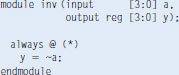
Bitwise operators act on single-bit signals or on multi-bit busses. For example, the inv module in HDL Example 4.2 describes four inverters connected to 4-bit busses.
Verilog
a[3:0] represents a 4-bit bus. The bits, from most significant to least significant, are a[3], a[2], a[1], and a[0]. This is called little-endian order, because the least significant bit has the smallest bit number. We could have named the bus a[4:1], in which case a[4] would have been the most significant. Or we could have used a[0:3], in which case the bits, from most significant to least significant, would be a[0], a[1], a[2], and a[3]. This is called big-endian order.
VHDL
VHDL uses STD_LOGIC_VECTOR, to indicate busses of STD_LOGIC. STD_LOGIC_VECTOR (3 downto 0) represents a 4-bit bus. The bits, from most significant to least significant, are 3, 2, 1, and 0. This is called little-endian order, because the least significant bit has the smallest bit number. We could have declared the bus to be STD_LOGIC_VECTOR (4 downto 1), in which case bit 4 would have been the most significant. Or we could have written STD_LOGIC_VECTOR (0 to 3), in which case the bits, from most significant to least significant, would be 0, 1, 2, and 3. This is called big-endian order.
The endianness of a bus is purely arbitrary. (See the sidebar in Section 6.2.2 for the origin of the term.) Indeed, endianness is also irrelevant to this example, because a bank of inverters doesn’t care what the order of the bits are. Endianness matters only for operators, such as addition, where the sum of one column carries over into the next. Either ordering is acceptable, as long as it is used consistently. We will consistently use the little-endian order, [N - 1:0] in Verilog and (N - 1 downto 0) in VHDL, for an N-bit bus.
After each code example in this chapter is a schematic produced from the Verilog code by the Synplify Pro synthesis tool. Figure 4.3 shows that the inv module synthesizes to a bank of four inverters, indicated by the inverter symbol labeled y[3:0]. The bank of inverters connects to 4-bit input and output busses. Similar hardware is produced from the synthesized VHDL code.
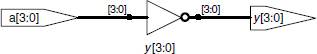
Figure 4.3 inv synthesized circuit
The gates module in HDL Example 4.3 demonstrates bitwise operations acting on 4-bit busses for other basic logic functions.
Verilog

![]() , and | are examples of Verilog operators, whereas a, b, and y1 are operands. A combination of operators and operands, such as
, and | are examples of Verilog operators, whereas a, b, and y1 are operands. A combination of operators and operands, such as a & b, or ∼(a | b), is called an expression. A complete command such as assign y4 = ∼(a & b); is called a statement.
assign out = in1 op in2; is called a continuous assignment statement. Continuous assignment statements end with a semicolon. Anytime the inputs on the right side of the = in a continuous assignment statement change, the output on the left side is recomputed. Thus, continuous assignment statements describe combinational logic.
VHDL
not, xor, and or are examples of VHDL operators, whereas a, b, and y1 are operands. A combination of operators and operands, such as a and b, or a nor b, is called an expression. A complete command such as y4 <= a nand b; is called a statement.
out <= in1 op in2; is called a concurrent signal assignment statement. VHDL assignment statements end with a semicolon. Anytime the inputs on the right side of the <= in a concurrent signal assignment statement change, the output on the left side is recomputed. Thus, concurrent signal assignment statements describe combinational logic.
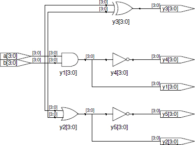
Figure 4.4 gates synthesized circuit
4.2.2 Comments and White Space
The gates example showed how to format comments. Verilog and VHDL are not picky about the use of white space (i.e., spaces, tabs, and line breaks). Nevertheless, proper indenting and use of blank lines is helpful to make nontrivial designs readable. Be consistent in your use of capitalization and underscores in signal and module names. Module and signal names must not begin with a digit.
Verilog
Verilog comments are just like those in C or Java. Comments beginning with /* continue, possibly across multiple lines, to the next */. Comments beginning with // continue to the end of the line.
Verilog is case-sensitive. y1 and Y1 are different signals in Verilog.
VHDL
VHDL comments begin with – and continue to the end of the line. Comments spanning multiple lines must use – at the beginning of each line.
VHDL is not case-sensitive. y1 and Y1 are the same signal in VHDL. However, other tools that may read your file might be case sensitive, leading to nasty bugs if you blithely mix upper and lower case.
4.2.3 Reduction Operators
Reduction operators imply a multiple-input gate acting on a single bus. HDL Example 4.4 describes an eight-input AND gate with inputs a7, a6,…, a0.
HDL Example 4.4 EIGHT-INPUT AND
Verilog

As one would expect, ![]() reduction operators are available for OR, XOR, NAND, and NOR as well. Recall that a multi-input XOR performs parity, returning TRUE if an odd number of inputs are TRUE.
reduction operators are available for OR, XOR, NAND, and NOR as well. Recall that a multi-input XOR performs parity, returning TRUE if an odd number of inputs are TRUE.
VHDL
VHDL does not have reduction operators. Instead, it provides the generate command (see Section 4.7). Alternatively, the operation can be written explicitly, as shown below.

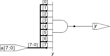
Figure 4.5 and8 synthesized circuit
4.2.4 Conditional Assignment
Conditional assignments select the output from among alternatives based on an input called the condition. HDL Example 4.5 illustrates a 2:1 multiplexer using conditional assignment.
HDL Example 4.5 2:1 MULTIPLEXER
Verilog
The conditional operator ?: chooses, based on a first expression, between a second and third expression. The first expression is called the condition. If the condition is 1, the operator chooses the second expression. If the condition is 0, the operator chooses the third expression.
?: is especially useful for describing a multiplexer because, based on the first input, it selects between two others. The following code demonstrates the idiom for a 2:1 multiplexer with 4-bit inputs and outputs using the conditional operator.

If s is 1, then y = d1. If s is 0, then y = d0.
?: is also called a ternary operator, because it takes three inputs. It is used for the same purpose in the C and Java programming languages.
VHDL
Conditional signal assignments perform different operations depending on some condition. They are especially useful for describing a multiplexer. For example, a 2:1 multiplexer can use conditional signal assignment to select one of two 4-bit inputs.
The conditional signal assignment sets y to d0 if s is 0. Otherwise it sets y to d1.
Figure 4.6 mux2 synthesized circuit
HDL Example 4.6 shows a 4:1 multiplexer based on the same principle as the 2:1 multiplexer in HDL Example 4.5.
Figure 4.7 shows the schematic for the 4:1 multiplexer produced by Synplify Pro. The software uses a different multiplexer symbol than this text has shown so far. The multiplexer has multiple data (d) and one-hot enable (e) inputs. When one of the enables is asserted, the associated data is passed to the output. For example, when s[1] = s[0] = 0, the bottom AND gate, un1_s_5, produces a 1, enabling the bottom input of the multiplexer and causing it to select d0[3:0].

Figure 4.7 mux4 synthesized circuit
HDL Example 4.6 4:1 MULTIPLEXER
Verilog
A 4:1 multiplexer can select one of four inputs using nested conditional operators.

If s[1] is 1, then the multiplexer chooses the first expression, (s[0] ? d3 : d2). This expression in turn chooses either d3 or d2 based on s[0] (y = d3 if s[0] is 1 and d2 if s[0] is 0). If s[1] is 0, then the multiplexer similarly chooses the second expression, which gives either d1 or d0 based on s[0].
VHDL
A 4:1 multiplexer can select one of four inputs using multiple else clauses in the conditional signal assignment.

VHDL also supports selected signal assignment statements to provide a shorthand when selecting from one of several possibilities. This is analogous to using a case statement in place of multiple if/else statements in some programming languages. The 4:1 multiplexer can be rewritten with selected signal assignment as follows:

![]()
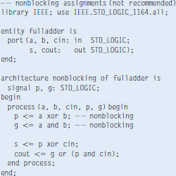
If we define intermediate signals, P and G,
![]()
we can rewrite the full adder as follows:
![]()
P and G are called internal variables, because they are neither inputs nor outputs but are used only internal to the module. They are similar to local variables in programming languages. HDL Example 4.7 shows how they are used in HDLs.
HDL assignment statements (assign in Verilog and <= in VHDL) take place concurrently. This is different from conventional programming languages such as C or Java, in which statements are evaluated in the order in which they are written. In a conventional language, it is important that S = P ![]() Cin comes after P = A
Cin comes after P = A ![]() B, because statements are executed sequentially. In an HDL, the order does not matter. Like hardware, HDL assignment statements are evaluated any time the inputs, signals on the right hand side, change their value, regardless of the order in which the assignment statements appear in a module.
B, because statements are executed sequentially. In an HDL, the order does not matter. Like hardware, HDL assignment statements are evaluated any time the inputs, signals on the right hand side, change their value, regardless of the order in which the assignment statements appear in a module.
Check this by filling out the truth table to convince yourself it is correct.
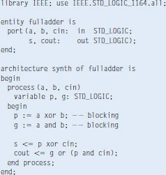
HDL Example 4.7 FULL ADDER
Verilog
In Verilog, wires are used to represent internal variables whose values are defined by assign statements such as assign p = a b; Wires technically have to be declared only for multibit busses, but it is good practice to include them for all internal variables; their declaration could have been omitted in this example.![]()

VHDL
In VHDL, signals are used to represent internal variables whose values are defined by concurrent signal assignment statements such as p <= a xor b;

4.2.6 Precedence
Notice that we parenthesized the cout computation in HDL Example 4.7 to define the order of operations as Cout = G + (P · Cin), rather than Cout = (G + P) · Cin. If we had not used parentheses, the default operation order is defined by the language. HDL Example 4.8 specifies operator precedence from highest to lowest for each language. The tables include arithmetic, shift, and comparison operators that will be defined in Chapter 5.
HDL Example 4.8 OPERATOR PRECEDENCE
Verilog
Table 4.1 Verilog operator precedence

The operator precedence for Verilog is much like you would expect in other programming languages. In particular, AND has precedence over OR. We could take advantage of this precedence to eliminate the parentheses.
assign cout = g | p & cin;
VHDL
Table 4.2 VHDL operator precedence

Multiplication has precedence over addition in VHDL, as you would expect. However, unlike Verilog, all of the logical operations (and, or, etc.) have equal precedence, unlike what one might expect in Boolean algebra. Thus, parentheses are necessary; otherwise cout <= g or p and cin would be interpreted from left to right as cout <= (g or p) and cin.
4.2.7 Numbers
Numbers can be specified in a variety of bases. Underscores in numbers are ignored and can be helpful in breaking long numbers into more readable chunks. HDL Example 4.9 explains how numbers are written in each language.
4.2.8 Z’s and X’s
HDLs use z to indicate a floating value. z is particularly useful for describing a tristate buffer, whose output floats when the enable is 0. Recall from Section 2.6 that a bus can be driven by several tristate buffers, exactly one of which should be enabled. HDL Example 4.10 shows the idiom for a tristate buffer. If the buffer is enabled, the output is the same as the input. If the buffer is disabled, the output is assigned a floating value (z).
Verilog
Verilog numbers can specify their base and size (the number of bits used to represent them). The format for declaring constants is N’Bvalue, where N is the size in bits, B is the base, and value gives the value. For example 9’h25 indicates a 9-bit number with a value of 2516 = 3710 = 0001001012. Verilog supports ’b for binary (base 2), ’o for octal (base 8), ’d for decimal (base 10), and ’h for hexadecimal (base 16). If the base is omitted, the base defaults to decimal.
If the size is not given, the number is assumed to have as many bits as the expression in which it is being used. Zeros are automatically padded on the front of the number to bring it up to full size. For example, if w is a 6-bit bus, assign w = ’b11 gives w the value 000011. It is better practice to explicitly give the size.
Table 4.3 Verilog numbers

VHDL
In VHDL, STD_LOGIC numbers are written in binary and enclosed in single quotes: ‘0’ and ‘1’ indicate logic 0 and 1.
STD_LOGIC_VECTOR numbers are written in binary or hexadecimal and enclosed in double quotation marks. The base is binary by default and can be explicitly defined with the prefix X for hexadecimal or B for binary.
Table 4.4 VHDL numbers
HDL Example 4.10 TRISTATE BUFFER
Verilog
VHDL

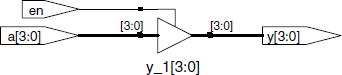
Figure 4.9 tristate synthesized circuit
Similarly, HDLs use x to indicate an invalid logic level. If a bus is simultaneously driven to 0 and 1 by two enabled tristate buffers (or other gates), the result is x, indicating contention. If all the tristate buffers driving a bus are simultaneously OFF, the bus will float, indicated by z.
At the start of simulation, state nodes such as flip-flop outputs are initialized to an unknown state (x in Verilog and u in VHDL). This is helpful to track errors caused by forgetting to reset a flip-flop before its output is used.
If a gate receives a floating input, it may produce an x output when it can’t determine the correct output value. Similarly, if it receives an illegal or uninitialized input, it may produce an x output. HDL Example 4.11 shows how Verilog and VHDL combine these different signal values in logic gates.
HDL Example 4.11 TRUTH TABLES WITH UNDEFINED AND FLOATING INPUTS
Verilog
Verilog signal values are 0, 1, z, and x. Verilog constants starting with z or x are padded with leading z’s or x’s (instead of 0’s) to reach their full length when necessary.
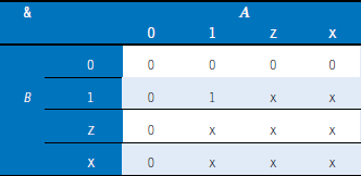
Table 4.5 shows a truth table for an AND gate using all four possible signal values. Note that the gate can sometimes determine the output despite some inputs being unknown. For example 0 & z returns 0 because the output of an AND gate is always 0 if either input is 0. Otherwise, floating or invalid inputs cause invalid outputs, displayed as x in Verilog.
Table 4.5 Verilog AND gate truth table with z and x
VHDL
VHDL STD_LOGIC signals are ‘0’, ‘1’, ‘z’, ‘x’, and ‘u’.
Table 4.6 shows a truth table for an AND gate using all five possible signal values. Notice that the gate can sometimes determine the output despite some inputs being unknown. For example, ‘0’ and ‘z’ returns ‘0’ because the output of an AND gate is always ‘0’ if either input is ‘0.’ Otherwise, floating or invalid inputs cause invalid outputs, displayed as ‘x’ in VHDL. Uninitialized inputs cause uninitialized outputs, displayed as ‘u’ in VHDL.
Table 4.6 VHDL AND gate truth table with z, x, and u

HDL Example 4.12 BIT SWIZZLING
Verilog
assign y = {c[2:1], {3{d[0]}}, c[0], 3’b101};
The {} operator is used to concatenate busses. {3{d[0]}} indicates three copies of d[0].
Don’t confuse the 3-bit binary constant 3’b101 with a bus named b. Note that it was critical to specify the length of 3 bits in the constant; otherwise, it would have had an unknown number of leading zeros that might appear in the middle of y.
If y were wider than 9 bits, zeros would be placed in the most significant bits.
VHDL
The & operator is used to concatenate busses. y must be a 9-bit STD_LOGIC_VECTOR. Do not confuse & with the and operator in VHDL.
Seeing x or u values in simulation is almost always an indication of a bug or bad coding practice. In the synthesized circuit, this corresponds to a floating gate input, uninitialized state, or contention. The x or u may be interpreted randomly by the circuit as 0 or 1, leading to unpredictable behavior.
4.2.9 Bit Swizzling
Often it is necessary to operate on a subset of a bus or to concatenate (join together) signals to form busses. These operations are collectively known as bit swizzling. In HDL Example 4.12, y is given the 9-bit value c2c1d0d0d0c0101 using bit swizzling operations.
4.2.10 Delays
HDL statements may be associated with delays specified in arbitrary units. They are helpful during simulation to predict how fast a circuit will work (if you specify meaningful delays) and also for debugging purposes to understand cause and effect (deducing the source of a bad output is tricky if all signals change simultaneously in the simulation results). These delays are ignored during synthesis; the delay of a gate produced by the synthesizer depends on its tpd and tcd specifications, not on numbers in HDL code.
HDL Example 4.13 adds delays to the original function from HDL Example 4.1, ![]() . It assumes that inverters have a delay of 1 ns, three-input AND gates have a delay of 2 ns, and three-input OR gates have a delay of 4 ns. Figure 4.10 shows the simulation waveforms, with y lagging 7 ns after the inputs. Note that y is initially unknown at the beginning of the simulation.
. It assumes that inverters have a delay of 1 ns, three-input AND gates have a delay of 2 ns, and three-input OR gates have a delay of 4 ns. Figure 4.10 shows the simulation waveforms, with y lagging 7 ns after the inputs. Note that y is initially unknown at the beginning of the simulation.
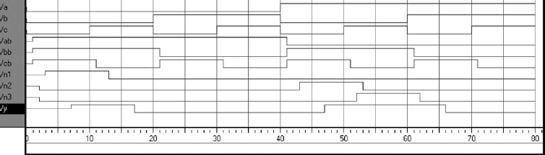
Figure 4.10 Example simulation waveforms with delays (from the ModelSim simulator)
HDL Example 4.13 LOGIC GATES WITH DELAYS
Verilog

Verilog files can include a timescale directive that indicates the value of each time unit. The statement is of the form ‘timescale unit/precision. In this file, each unit is 1 ns, and the simulation has 1 ps precision. If no timescale directive is given in the file, a default unit and precision (usually 1 ns for both) is used. In Verilog, a # symbol is used to indicate the number of units of delay. It can be placed in assign statements, as well as non-blocking (<) and blocking (=) assignments, which will be discussed in Section 4.5.4.
VHDL

In VHDL, the after clause is used to indicate delay. The units, in this case, are specified as nanoseconds.
4.2.11 VHDL Libraries and Types*
(This section may be skipped by Verilog users.) Unlike Verilog, VHDL enforces a strict data typing system that can protect the user from some errors but that is also clumsy at times.
Despite its fundamental importance, the STD_LOGIC type is not built into VHDL. Instead, it is part of the IEEE.STD_LOGIC_1164 library. Thus, every file must contain the library statements shown in the previous examples.
Moreover, IEEE.STD_LOGIC_1164 lacks basic operations such as addition, comparison, shifts, and conversion to integers for the STD_LOGIC_VECTOR data. Most CAD vendors have adopted yet more libraries containing these functions: IEEE.STD_LOGIC_UNSIGNED and IEEE.STD_LOGIC_SIGNED. See Section 1.4 for a discussion of unsigned and signed numbers and examples of these operations.
VHDL also has a BOOLEAN type with two values: true and false. BOOLEAN values are returned by comparisons (such as the equality comparison, s = ‘0’) and are used in conditional statements such as when. Despite the temptation to believe a BOOLEAN true value should be equivalent to a STD_LOGIC ‘1’ and BOOLEAN false should mean STD_LOGIC ‘0’, these types are not interchangeable. Thus, the following code is illegal:
y <= d1 when s else d0;
q <= (state = S2);
Instead, we must write
y <= d1 when (s = ‘1’) else d0;
q <= ‘1’ when (state = S2) else ‘0’;
Although we do not declare any signals to be BOOLEAN, they are automatically implied by comparisons and used by conditional statements.
Similarly, VHDL has an INTEGER type that represents both positive and negative integers. Signals of type INTEGER span at least the values -231 to 231 - 1. Integer values are used as indices of busses. For example, in the statement
y <= a(3) and a(2) and a(1) and a(0);
0, 1, 2, and 3 are integers serving as an index to choose bits of the a signal. We cannot directly index a bus with a STD_LOGIC or STD_LOGIC_VECTOR signal. Instead, we must convert the signal to an INTEGER. This is demonstrated in HDL Example 4.14 for an 8:1 multiplexer that selects one bit from a vector using a 3-bit index. The CONV_INTEGER function is defined in the IEEE.STD_LOGIC_UNSIGNED library and performs the conversion from STD_LOGIC_VECTOR to INTEGER for positive (unsigned) values.
VHDL is also strict about out ports being exclusively for output. For example, the following code for two and three-input AND gates is illegal VHDL because v is an output and is also used to compute w.

VHDL defines a special port type, buffer, to solve this problem. A signal connected to a buffer port behaves as an output but may also be used within the module. The corrected entity definition follows. Verilog does not have this limitation and does not require buffer ports.

VHDL supports enumeration types as an abstract way of representing information without assigning specific binary encodings. For example, the divide-by-3 FSM described in Section 3.4.2 uses three states. We can give the states names using the enumeration type rather than referring to them by binary values. This is powerful because it allows VHDL to search for the best state encoding during synthesis, rather than depending on an arbitrary encoding specified by the user.
type statetype is (S0, S1, S2);
signal state, nextstate: statetype;
4.3 STRUCTURAL MODELING
The previous section discussed behavioral modeling, describing a module in terms of the relationships between inputs and outputs. This section examines structural modeling, describing a module in terms of how it is composed of simpler modules.

Figure 4.11 mux8 synthesized circuit
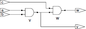
Figure 4.12 and23 synthesized circuit
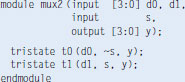
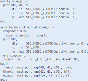
For example, HDL Example 4.15 shows how to assemble a 4:1 multiplexer from three 2:1 multiplexers. Each copy of the 2:1 multiplexer is called an instance. Multiple instances of the same module are distinguished by distinct names, in this case lowmux, highmux, and finalmux. This is an example of regularity, in which the 2:1 multiplexer is reused many times.
HDL Example 4.15 STRUCTURAL MODEL OF 4:1 MULTIPLEXER
Verilog

The three mux2 instances are called lowmux, highmux, and finalmux. The mux2 module must be defined elsewhere in the Verilog code.
VHDL
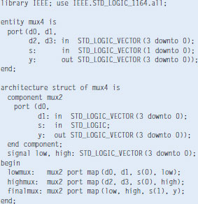
The architecture must first declare the mux2 ports using the component declaration statement. This allows VHDL tools to check that the component you wish to use has the same ports as the entity that was declared somewhere else in another entity statement, preventing errors caused by changing the entity but not the instance. However, component declaration makes VHDL code rather cumbersome.
Note that this architecture of mux4 was named struct, whereas architectures of modules with behavioral descriptions from Section 4.2 were named synth. VHDL allows multiple architectures (implementations) for the same entity; the architectures are distinguished by name. The names themselves have no significance to the CAD tools, but struct and synth are common. Synthesizable VHDL code generally contains only one architecture for each entity, so we will not discuss the VHDL syntax to configure which architecture is used when multiple architectures are defined.

Figure 4.13 mux4 synthesized circuit
HDL Example 4.16 uses structural modeling to construct a 2:1 multiplexer from a pair of tristate buffers.
HDL Example 4.16 STRUCTURAL MODEL OF 2:1 MULTIPLEXER
Verilog
In Verilog, expressions such as ∼s are permitted in the port list for an instance. Arbitrarily complicated expressions are legal but discouraged because they make the code difficult to read.
VHDL

In VHDL, expressions such as not s are not permitted in the port map for an instance. Thus, sbar must be defined as a separate signal.

HDL Example 4.17 shows how modules can access part of a bus. An 8-bit wide 2:1 multiplexer is built using two of the 4-bit 2:1 multiplexers already defined, operating on the low and high nibbles of the byte.
In general, complex systems are designed hierarchically. The overall system is described structurally by instantiating its major components. Each of these components is described structurally from its building blocks, and so forth recursively until the pieces are simple enough to describe behaviorally. It is good style to avoid (or at least to minimize) mixing structural and behavioral descriptions within a single module.
HDL Example 4.17 ACCESSING PARTS OF BUSSES
Verilog

VHDL

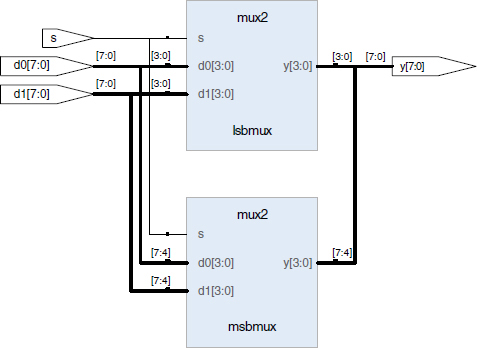
Figure 4.15 mux2_8 synthesized circuit
4.4 SEQUENTIAL LOGIC
HDL synthesizers recognize certain idioms and turn them into specific sequential circuits. Other coding styles may simulate correctly but synthesize into circuits with blatant or subtle errors. This section presents the proper idioms to describe registers and latches.
4.4.1 Registers
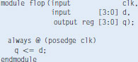
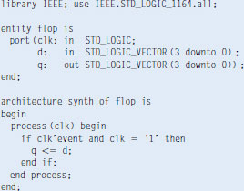
The vast majority of modern commercial systems are built with registers using positive edge-triggered D flip-flops. HDL Example 4.18 shows the idiom for such flip-flops.
In Verilog always statements and VHDL process statements, signals keep their old value until an event in the sensitivity list takes place that explicitly causes them to change. Hence, such code, with appropriate sensitivity lists, can be used to describe sequential circuits with memory. For example, the flip-flop includes only clk in the sensitive list. It remembers its old value of q until the next rising edge of the clk, even if d changes in the interim.
In contrast, Verilog continuous assignment statements (assign) and VHDL concurrent assignment statements (<=) are reevaluated anytime any of the inputs on the right hand side changes. Therefore, such code necessarily describes combinational logic.
Verilog
A Verilog always statement is written in the form
The statement is executed only when the event specified in the sensitivity list occurs. In this example, the statement is q <= d (pronounced “q gets d”). Hence, the flip-flop copies d to q on the positive edge of the clock and otherwise remembers the old state of q.
<= is called a nonblocking assignment. Think of it as a regular = sign for now; we’ll return to the more subtle points in Section 4.5.4. Note that <= is used instead of assign inside an always statement.
All signals on the left hand side of <= or = in an always statement must be declared as reg. In this example, q is both an output and a reg, so it is declared as output reg [3:0] q. Declaring a signal as reg does not mean the signal is actually the output of a register! All it means is that the signal appears on the left hand side of an assignment in an always statement. We will see later examples of always statements describing combinational logic in which the output is declared reg but does not come from a flip-flop.
VHDL
A VHDL process is written in the form
The statement is executed when any of the variables in the sensitivity list change. In this example, the if statement is executed when clk changes, indicated by clk’event. If the change is a rising edge (clk = ‘1’ after the event), then q <= d (pronounced “q gets d”). Hence, the flip-flop copies d to q on the positive edge of the clock and otherwise remembers the old state of q.
An alternative VHDL idiom for a flip-flop is
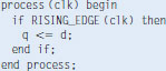
RISING_EDGE (clk) is synonymous with clk’event and clk = 1.
Figure 4.16 flop synthesized circuit
4.4.2 Resettable Registers
When simulation begins or power is first applied to a circuit, the output of a flop or register is unknown. This is indicated with x in Verilog and ‘u’ in VHDL. Generally, it is good practice to use resettable registers so that on powerup you can put your system in a known state. The reset may be either asynchronous or synchronous. Recall that asynchronous reset occurs immediately, whereas synchronous reset clears the output only on the next rising edge of the clock. HDL Example 4.19 demonstrates the idioms for flip-flops with asynchronous and synchronous resets. Note that distinguishing synchronous and asynchronous reset in a schematic can be difficult. The schematic produced by Synplify Pro places asynchronous reset at the bottom of a flip-flop and synchronous reset on the left side.
HDL Example 4.19 RESETTABLE REGISTER
Verilog
Multiple signals in an always statement sensitivity list are separated with a comma or the word or. Notice that posedge reset is in the sensitivity list on the asynchronously resettable flop, but not on the synchronously resettable flop. Thus, the asynchronously resettable flop immediately responds to a rising edge on reset, but the synchronously resettable flop responds to reset only on the rising edge of the clock.
Because the modules have the same name, flopr, you may include only one or the other in your design.
VHDL

Multiple signals in a process sensitivity list are separated with a comma. Notice that reset is in the sensitivity list on the asynchronously resettable flop, but not on the synchronously resettable flop. Thus, the asynchronously resettable flop immediately responds to a rising edge on reset, but the synchronously resettable flop responds to reset only on the rising edge of the clock.
Recall that the state of a flop is initialized to ‘u’ at startup during VHDL simulation.
As mentioned earlier, the name of the architecture (asynchronous or synchronous, in this example) is ignored by the VHDL tools but may be helpful to the human reading the code. Because both architectures describe the entity flopr, you may include only one or the other in your design.
Figure 4.17 flopr synthesized circuit (a) asynchronous reset, (b) synchronous reset
4.4.3 Enabled Registers
Enabled registers respond to the clock only when the enable is asserted. HDL Example 4.20 shows an asynchronously resettable enabled register that retains its old value if both reset and en are FALSE.
HDL Example 4.20 RESETTABLE ENABLED REGISTER
Verilog
VHDL
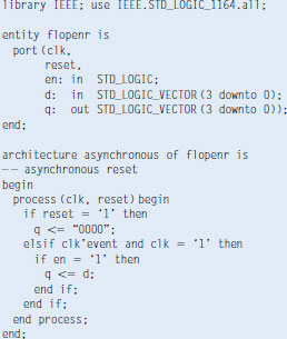

Figure 4.18 flopenr synthesized circuit
4.4.4 Multiple Registers
A single always/process statement can be used to describe multiple pieces of hardware. For example, consider the synchronizer from Section 3.5.5 made of two back-to-back flip-flops, as shown in Figure 4.19. HDL Example 4.21 describes the synchronizer. On the rising edge of clk, d is copied to n1. At the same time, n1 is copied to q.
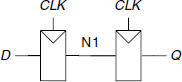
Figure 4.19 Synchronizer circuit
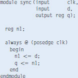
HDL Example 4.21 SYNCHRONIZER
Verilog
n1 must be declared as a reg because it is an internal signal used on the left hand side of <= in an always statement. Also notice that the begin/end construct is necessary because multiple statements appear in the always statement. This is analogous to { } in C or Java. The begin/end was not needed in the flopr example because if/else counts as a single statement.
VHDL
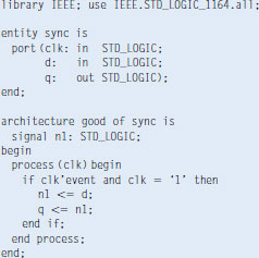
n1 must be declared as a signal because it is an internal signal used in the module.
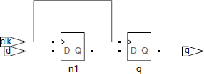
Figure 4.20 sync synthesized circuit
4.4.5 Latches
Recall from Section 3.2.2 that a D latch is transparent when the clock is HIGH, allowing data to flow from input to output. The latch becomes opaque when the clock is LOW, retaining its old state. HDL Example 4.22 shows the idiom for a D latch.
Not all synthesis tools support latches well. Unless you know that your tool does support latches and you have a good reason to use them, avoid them and use edge-triggered flip-flops instead. Furthermore, take care that your HDL does not imply any unintended latches, something that is easy to do if you aren’t attentive. Many synthesis tools warn you when a latch is created; if you didn’t expect one, track down the bug in your HDL.
4.5 MORE COMBINATIONAL LOGIC
In Section 4.2, we used assignment statements to describe combinational logic behaviorally. Verilog always statements and VHDL process statements are used to describe sequential circuits, because they remember the old state when no new state is prescribed. However, always/process statements can also be used to describe combinational logic behaviorally if the sensitivity list is written to respond to changes in all of the inputs and the body prescribes the output value for every possible input combination. HDL Example 4.23 uses always/process statements to describe a bank of four inverters (see Figure 4.3 for the synthesized circuit).
HDL Example 4.22 D LATCH
Verilog
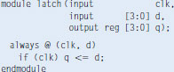
The sensitivity list contains both clk and d, so the always statement evaluates any time clk or d changes. If clk is HIGH, d flows through to q.
q must be declared to be a reg because it appears on the left hand side of <= in an always statement. This does not always mean that q is the output of a register.
VHDL
The sensitivity list contains both clk and d, so the process evaluates anytime clk or d changes. If clk is HIGH, d flows through to q.
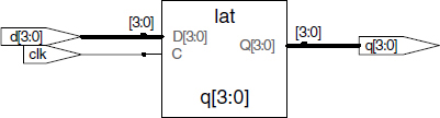
Figure 4.21 latch synthesized circuit
HDL Example 4.23 INVERTER USING always/process
Verilog
always @ (*) reevaluates the statements inside the always statement any time any of the signals on the right hand side of <= or = inside the always statement change. Thus, @ (*) is a safe way to model combinational logic. In this particular example, @ (a) would also have sufficed.
The = in the always statement is called a blocking assignment, in contrast to the <= nonblocking assignment. In Verilog, it is good practice to use blocking assignments for combinational logic and nonblocking assignments for sequential logic. This will be discussed further in Section 4.5.4.
Note that y must be declared as reg because it appears on the left hand side of a <= or = sign in an always statement. Nevertheless, y is the output of combinational logic, not a register.
VHDL

The begin and end process statements are required in VHDL even though the process contains only one assignment.
HDLs support blocking and nonblocking assignments in an always/process statement. A group of blocking assignments are evaluated in the order in which they appear in the code, just as one would expect in a standard programming language. A group of nonblocking assignments are evaluated concurrently; all of the statements are evaluated before any of the signals on the left hand sides are updated.
HDL Example 4.24 defines a full adder using intermediate signals p and g to compute s and cout. It produces the same circuit from Figure 4.8, but uses always/process statements in place of assignment statements.

Figure 4.8 fulladder synthesized circuit
These two examples are poor applications of always/process statements for modeling combinational logic because they require more lines than the equivalent approach with assignment statements from Section 4.2.1. Moreover, they pose the risk of inadvertently implying sequential logic if the inputs are left out of the sensitivity list. However, case and if statements are convenient for modeling more complicated combinational logic. case and if statements must appear within always/process statements and are examined in the next sections.
Verilog
In a Verilog always statement, = indicates a blocking assignment and <= indicates a nonblocking assignment (also called a concurrent assignment).
Do not confuse either type with continuous assignment using the assign statement. assign statements must be used outside always statements and are also evaluated concurrently.
VHDL
In a VHDL process statement, : = indicates a blocking assignment and <= indicates a nonblocking assignment (also called a concurrent assignment). This is the first section where : = is introduced.
Nonblocking assignments are made to outputs and to signals. Blocking assignments are made to variables, which are declared in process statements (see HDL Example 4.24).
<= can also appear outside process statements, where it is also evaluated concurrently.
HDL Example 4.24 FULL ADDER USING always/process
Verilog

In this case, an @ (a, b, cin) would have been equivalent to @ (*). However, @ (*) is better because it avoids common mistakes of missing signals in the stimulus list.
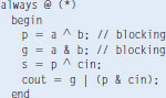
For reasons that will be discussed in Section 4.5.4, it is best to use blocking assignments for combinational logic. This example uses blocking assignments, first computing p, then g, then s, and finally cout.
Because p and g appear on the left hand side of an assignment in an always statement, they must be declared to be reg.
VHDL
The process sensitivity list must include a, b and cin because combinational logic should respond to changes of any input.
For reasons that will be discussed in Section 4.5.4, it is best to use blocking assignments for intermediate variables in combinational logic. This example uses blocking assignments for p and g so that they get their new values before being used to compute s and cout that depend on them.
Because p and g appear on the left hand side of a blocking assignment (:=) in a process statement, they must be declared to be variable rather than signal. The variable declaration appears before the begin in the process where the variable is used.
4.5.1 Case Statements
A better application of using the always/process statement for combinational logic is a seven-segment display decoder that takes advantage of the case statement that must appear inside an always/process statement.
As you might have noticed in Example 2.10, the design process for large blocks of combinational logic is tedious and prone to error. HDLs offer a great improvement, allowing you to specify the function at a higher level of abstraction, and then automatically synthesize the function into gates. HDL Example 4.25 uses case statements to describe a seven-segment display decoder based on its truth table. (See Example 2.10 for a description of the seven-segment display decoder.) The case statement performs different actions depending on the value of its input. A case statement implies combinational logic if all possible input combinations are defined; otherwise it implies sequential logic, because the output will keep its old value in the undefined cases.
HDL Example 4.25 SEVEN-SEGMENT DISPLAY DECODER
Verilog
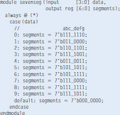
The case statement checks the value of data. When data is 0, the statement performs the action after the colon, setting segments to 1111110. The case statement similarly checks other data values up to 9 (note the use of the default base, base 10).
The default clause is a convenient way to define the output for all cases not explicitly listed, guaranteeing combinational logic.
In Verilog, case statements must appear inside always statements.
VHDL

The case statement checks the value of data. When data is 0, the statement performs the action after the =>, setting segments to 1111110. The case statement similarly checks other data values up to 9 (note the use of X for hexadecimal numbers). The others clause is a convenient way to define the output for all cases not explicitly listed, guaranteeing combinational logic.
Unlike Verilog, VHDL supports selected signal assignment statements (see HDL Example 4.6), which are much like case statements but can appear outside processes. Thus, there is less reason to use processes to describe combinational logic.
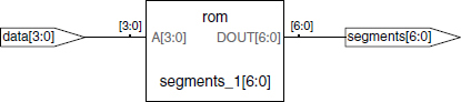
Figure 4.22 sevenseg synthesized circuit
Synplify Pro synthesizes the seven-segment display decoder into a read-only memory (ROM) containing the 7 outputs for each of the 16 possible inputs. ROMs are discussed further in Section 5.5.6.
If the default or others clause were left out of the case statement, the decoder would have remembered its previous output anytime data were in the range of 10–15. This is strange behavior for hardware.
Ordinary decoders are also commonly written with case statements. HDL Example 4.26 describes a 3:8 decoder.
4.5.2 If Statements
always/process statements may also contain if statements. The if statement may be followed by an else statement. If all possible input combinations are handled, the statement implies combinational logic; otherwise, it produces sequential logic (like the latch in Section 4.4.5).
HDL Example 4.26 3:8 DECODER
Verilog
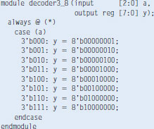
No default statement is needed because all cases are covered.
VHDL
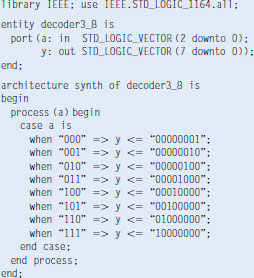
No others clause is needed because all cases are covered.

Figure 4.23 decoder3_8 synthesized circuit
HDL Example 4.27 PRIORITY CIRCUIT
Verilog

In Verilog, if statements must appear inside of always statements.
VHDL
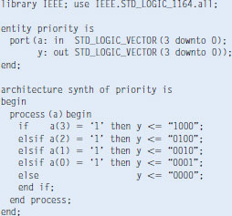
Unlike Verilog, VHDL supports conditional signal assignment statements (see HDL Example 4.6), which are much like if statements but can appear outside processes. Thus, there is less reason to use processes to describe combinational logic. (Figure follows on next page.)
HDL Example 4.27 uses if statements to describe a priority circuit, defined in Section 2.4. Recall that an N-input priority circuit sets the output TRUE that corresponds to the most significant input that is TRUE.
4.5.3 Verilog casez*
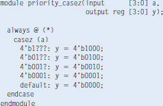
(This section may be skipped by VHDL users.) Verilog also provides the casez statement to describe truth tables with don’t cares (indicated with ? in the casez statement). HDL Example 4.28 shows how to describe a priority circuit with casez.
Synplify Pro synthesizes a slightly different circuit for this module, shown in Figure 4.25, than it did for the priority circuit in Figure 4.24. However, the circuits are logically equivalent.
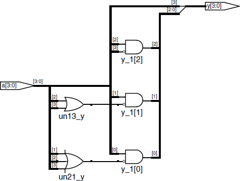
Figure 4.24 priority synthesized circuit
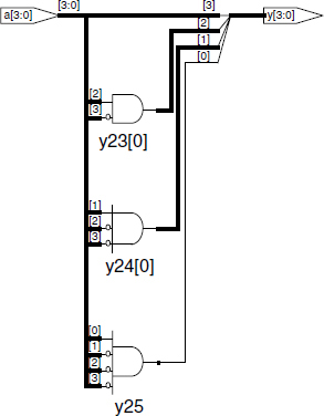
Figure 4.25 priority_casez synthesized circuit
4.5.4 Blocking and Nonblocking Assignments
The guidelines on page 203 explain when and how to use each type of assignment. If these guidelines are not followed, it is possible to write code that appears to work in simulation but synthesizes to incorrect hardware. The optional remainder of this section explains the principles behind the guidelines.
Combinational Logic*
The full adder from HDL Example 4.24 is correctly modeled using blocking assignments. This section explores how it operates and how it would differ if nonblocking assignments had been used.
Imagine that a, b, and cin are all initially 0. p, g, s, and cout are thus 0 as well. At some time, a changes to 1, triggering the always/process statement. The four blocking assignments evaluate in the order shown here. (In the VHDL code, s and cout are assigned concurrently.) Note that p and g get their new values before s and cout are computed because of the blocking assignments. This is important because we want to compute s and cout using the new values of p and g.
BLOCKING AND NONBLOCKING ASSIGNMENT GUIDELINES
Verilog
always @ (posedge clk) and nonblocking assignments to model synchronous sequential logic.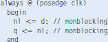
assign y = s ? d1 : d0;
VHDL
process (in1, in2, … ) to model more complicated combinational logic where the process is helpful. Use blocking assignments for internal variables.
In contrast, HDL Example 4.29 illustrates the use of nonblocking assignments.
Now consider the same case of a rising from 0 to 1 while b and cin are 0. The four nonblocking assignments evaluate concurrently:
Observe that s is computed concurrently with p and hence uses the old value of p, not the new value. Therefore, s remains 0 rather than becoming 1. However, p does change from 0 to 1. This change triggers the always/process statement to evaluate a second time, as follows:
HDL Example 4.29 FULL ADDER USING NONBLOCKING ASSIGNMENTS
Verilog

Because p and g appear on the left hand side of an assignment in an always statement, they must be declared to be reg.
VHDL
Because p and g appear on the left hand side of a nonblocking assignment in a process statement, they must be declared to be signal rather than variable. The signal declaration appears before the begin in the architecture, not the process.
This time, p is already 1, so s correctly changes to 1. The nonblocking assignments eventually reach the right answer, but the always/process statement had to evaluate twice. This makes simulation slower, though it synthesizes to the same hardware.
Another drawback of nonblocking assignments in modeling combinational logic is that the HDL will produce the wrong result if you forget to include the intermediate variables in the sensitivity list.
Verilog
If the sensitivity list of the always statement in HDL Example 4.29 were written as always @ (a, b, cin) rather than always @ (*), then the statement would not reevaluate when p or g changes. In the previous example, s would be incorrectly left at 0, not 1.
VHDL
If the sensitivity list of the process statement in HDL Example 4.29 were written as process (a, b, cin) rather than process (a, b, cin, p, g), then the statement would not reevaluate when p or g changes. In the previous example, s would be incorrectly left at 0, not 1.
Worse yet, some synthesis tools will synthesize the correct hardware even when a faulty sensitivity list causes incorrect simulation. This leads to a mismatch between the simulation results and what the hardware actually does.
Sequential Logic*
The synchronizer from HDL Example 4.21 is correctly modeled using non-blocking assignments. On the rising edge of the clock, d is copied to n1 at the same time that n1 is copied to q, so the code properly describes two registers. For example, suppose initially that d = 0, n1 = 1, and q = 0. On the rising edge of the clock, the following two assignments occur concurrently, so that after the clock edge, n1 = 0 and q = 1.
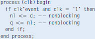
HDL Example 4.30 tries to describe the same module using blocking assignments. On the rising edge of clk, d is copied to n1. Then this new value of n1 is copied to q, resulting in d improperly appearing at both n1 and q. The assignments occur one after the other so that after the clock edge, q = n1 = 0.
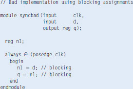
Because n1 is invisible to the outside world and does not influence the behavior of q, the synthesizer optimizes it away entirely, as shown in Figure 4.26.

Figure 4.26 syncbad synthesized circuit
The moral of this illustration is to exclusively use nonblocking assignment in always statements when modeling sequential logic. With sufficient cleverness, such as reversing the orders of the assignments, you could make blocking assignments work correctly, but blocking assignments offer no advantages and only introduce the risk of unintended behavior. Certain sequential circuits will not work with blocking assignments no matter what the order.
4.6 FINITE STATE MACHINES
Recall that a finite state machine (FSM) consists of a state register and two blocks of combinational logic to compute the next state and the output given the current state and the input, as was shown in Figure 3.22. HDL descriptions of state machines are correspondingly divided into three parts to model the state register, the next state logic, and the output logic.
HDL Example 4.31 DIVIDE-BY-3 FINITE STATE MACHINE
Verilog
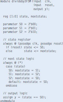
The parameter statement is used to define constants within a module. Naming the states with parameters is not required, but it makes changing state encodings much easier and makes the code more readable.
Notice how a case statement is used to define the state transition table. Because the next state logic should be combinational, a default is necessary even though the state 2’b11 should never arise.
The output, y, is 1 when the state is S0. The equality comparison a = = b evaluates to 1 if a equals b and 0 otherwise. The inequality comparison a != b does the inverse, evaluating to 1 if a does not equal b.
VHDL
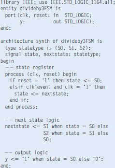
This example defines a new enumeration data type, statetype, with three possibilities: S0, S1, and S2. state and nextstate are statetype signals. By using an enumeration instead of choosing the state encoding, VHDL frees the synthesizer to explore various state encodings to choose the best one.
The output, y, is 1 when the state is S0. The inequality-comparison uses /=. To produce an output of 1 when the state is anything but S0, change the comparison to state /= S0.
HDL Example 4.31 describes the divide-by-3 FSM from Section 3.4.2. It provides an asynchronous reset to initialize the FSM. The state register uses the ordinary idiom for flip-flops. The next state and output logic blocks are combinational.
The Synplify Pro Synthesis tool just produces a block diagram and state transition diagram for state machines; it does not show the logic gates or the inputs and outputs on the arcs and states. Therefore, be careful that you have specified the FSM correctly in your HDL code. The state transition diagram in Figure 4.27 for the divide-by-3 FSM is analogous to the diagram in Figure 3.28(b). The double circle indicates that S0 is the reset state. Gate-level implementations of the divide-by-3 FSM were shown in Section 3.4.2.
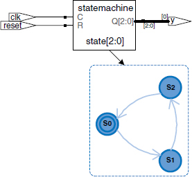
Figure 4.27 divideby3fsm synthesized circuit
Notice that the synthesis tool uses a 3-bit encoding (Q[2:0]) instead of the 2-bit encoding suggested in the Verilog code.
If, for some reason, we had wanted the output to be HIGH in states S0 and S1, the output logic would be modified as follows.
Verilog
VHDL
The next two examples describe the snail pattern recognizer FSM from Section 3.4.3. The code shows how to use case and if statements to handle next state and output logic that depend on the inputs as well as the current state. We show both Moore and Mealy modules. In the Moore machine (HDL Example 4.32), the output depends only on the current state, whereas in the Mealy machine (HDL Example 4.33), the output logic depends on both the current state and inputs.
HDL Example 4.32 PATTERN RECOGNIZER MOORE FSM
Verilog
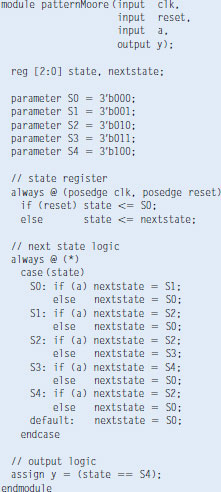
Note how nonblocking assignments (<=) are used in the state register to describe sequential logic, whereas blocking assignments (=) are used in the next state logic to describe combinational logic.
VHDL
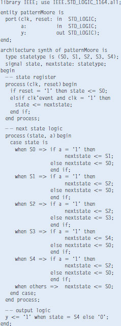
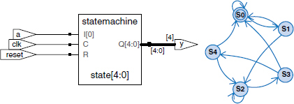
Figure 4.28 patternMoore synthesized circuit
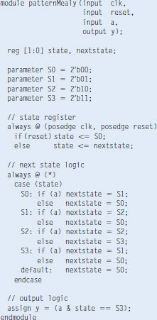
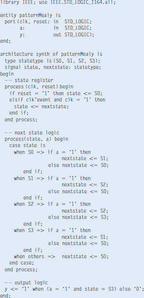
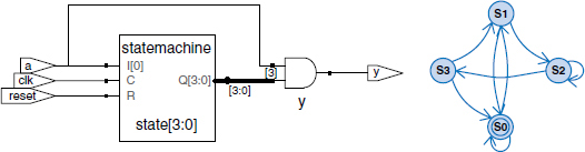
Figure 4.29 patternMealy synthesized circuit
4.7 PARAMETERIZED MODULES*
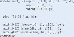
So far all of our modules have had fixed-width inputs and outputs. For example, we had to define separate modules for 4- and 8-bit wide 2:1 multiplexers. HDLs permit variable bit widths using parameterized modules. HDL Example 4.34 declares a parameterized 2:1 multiplexer with a default width of 8, then uses it to create 8- and 12-bit 4:1 multiplexers.
HDL Example 4.34 PARAMETERIZED N-BIT MULTIPLEXERS
Verilog
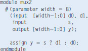
Verilog allows a # (parameter … ) statement before the inputs and outputs to define parameters. The parameter statement includes a default value (8) of the parameter, width. The number of bits in the inputs and outputs can depend on this parameter.
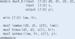
The 8-bit 4:1 multiplexer instantiates three 2:1 multiplexers using their default widths.
In contrast, a 12-bit 4:1 multiplexer, mux4_12, would need to override the default width using #() before the instance name, as shown below.
Do not confuse the use of the # sign indicating delays with the use of #( … ) in defining and overriding parameters.
VHDL

The generic statement includes a default value (8) of width.
The 8-bit 4:1 multiplexer, mux4_8, instantiates three 2:1 multiplexers using their default widths.
In contrast, a 12-bit 4:1 multiplexer, mux4_12, would need to override the default width using generic map, as shown below.
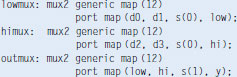
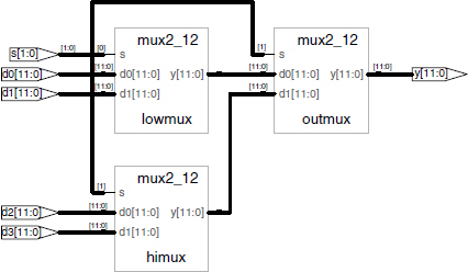
Figure 4.30 mux4_12 synthesized circuit
HDL Example 4.35 PARAMETERIZED N:2N DECODER
Verilog

VHDL
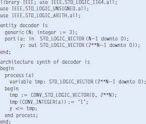
2**N indicates 2N.
CONV_STD_LOGIC_VECTOR(0, 2**N) produces a STD_LOGIC_VECTOR of length 2N containing all 0’s. It requires the STD_LOGIC_ARITH library. The function is useful in other parameterized functions, such as resettable flip-flops that need to be able to produce constants with a parameterized number of bits. The bit index in VHDL must be an integer, so the CONV_INTEGER function is used to convert a from a STD_LOGIC_VECTOR to an integer.
HDL Example 4.35 shows a decoder, which is an even better application of parameterized modules. A large N:2N decoder is cumbersome to specify with case statements, but easy using parameterized code that simply sets the appropriate output bit to 1. Specifically, the decoder uses blocking assignments to set all the bits to 0, then changes the appropriate bit to 1.
HDLs also provide generate statements to produce a variable amount of hardware depending on the value of a parameter. generate supports for loops and if statements to determine how many of what types of hardware to produce. HDL Example 4.36 demonstrates how to use generate statements to produce an N-input AND function from a cascade of two-input AND gates.
Use generate statements with caution; it is easy to produce a large amount of hardware unintentionally!
HDL Example 4.36 PARAMETERIZED N-INPUT AND GATE
Verilog
The for statement loops through i = 1, 2, …, width-1 to produce many consecutive AND gates. The begin in a generate for loop must be followed by a : and an arbitrary label (forloop, in this case).
Of course, writing assign y = &a would be much easier!
VHDL

Figure 4.31 andN synthesized circuit
4.8 TESTBENCHES
A testbench is an HDL module that is used to test another module, called the device under test (DUT). The testbench contains statements to apply inputs to the DUT and, ideally, to check that the correct outputs are produced. The input and desired output patterns are called test vectors.
Consider testing the sillyfunction module from Section 4.1.1 that computes ![]() . This is a simple module, so we can perform exhaustive testing by applying all eight possible test vectors.
. This is a simple module, so we can perform exhaustive testing by applying all eight possible test vectors.
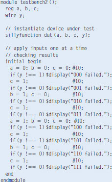
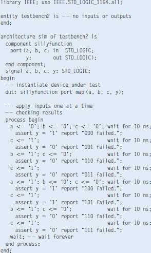
HDL Example 4.37 demonstrates a simple testbench. It instantiates the DUT, then applies the inputs. Blocking assignments and delays are used to apply the inputs in the appropriate order. The user must view the results of the simulation and verify by inspection that the correct outputs are produced. Testbenches are simulated the same as other HDL modules. However, they are not synthesizeable.
HDL Example 4.37 TESTBENCH
Verilog
The initial statement executes the statements in its body at the start of simulation. In this case, it first applies the input pattern 000 and waits for 10 time units. It then applies 001 and waits 10 more units, and so forth until all eight possible inputs have been applied. initial statements should be used only in testbenches for simulation, not in modules intended to be synthesized into actual hardware. Hardware has no way of magically executing a sequence of special steps when it is first turned on.
Like signals in always statements, signals in initial statements must be declared to be reg.
VHDL
The process statement first applies the input pattern 000 and waits for 10 ns. It then applies 001 and waits 10 more ns, and so forth until all eight possible inputs have been applied.
At the end, the process waits indefinitely; otherwise, the process would begin again, repeatedly applying the pattern of test vectors.
Checking for correct outputs is tedious and error-prone. Moreover, determining the correct outputs is much easier when the design is fresh in your mind; if you make minor changes and need to retest weeks later, determining the correct outputs becomes a hassle. A much better approach is to write a self-checking testbench, shown in HDL Example 4.38.
HDL Example 4.38 SELF-CHECKING TESTBENCH
Verilog
This module checks y against expectations after each input test vector is applied. In Verilog, comparison using == or != is effective between signals that do not take on the values of x and z. Testbenches use the === and !== operators for comparisons of equality and inequality, respectively, because these operators work correctly with operands that could be x or z. It uses the $display system task to print a message on the simulator console if an error occurs. $display is meaningful only in simulation, not synthesis.
VHDL
The assert statement checks a condition and prints the message given in the report clause if the condition is not satisfied. assert is meaningful only in simulation, not in synthesis.
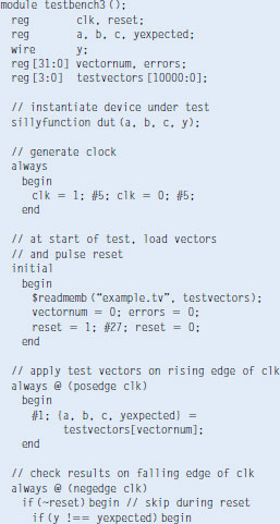
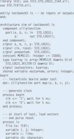
Writing code for each test vector also becomes tedious, especially for modules that require a large number of vectors. An even better approach is to place the test vectors in a separate file. The testbench simply reads the test vectors from the file, applies the input test vector to the DUT, waits, checks that the output values from the DUT match the output vector, and repeats until reaching the end of the test vectors file.
HDL Example 4.39 demonstrates such a testbench. The testbench generates a clock using an always/process statement with no stimulus list, so that it is continuously reevaluated. At the beginning of the simulation, it reads the test vectors from a text file and pulses reset for two cycles. example.tv is a text file containing the inputs and expected output written in binary:
000_1
001_0
010_0
011_0
100_1
101_1
110_0
111_0
HDL Example 4.39 TESTBENCH WITH TEST VECTOR FILE
Verilog
VHDL
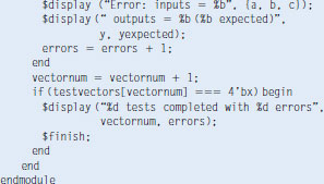
$readmemb reads a file of binary numbers into the testvectors array. $readmemh is similar but reads a file of hexadecimal numbers.
The next block of code waits one time unit after the rising edge of the clock (to avoid any confusion if clock and data change simultaneously), then sets the three inputs and the expected output based on the four bits in the current test vector. The next block of code checks the output of the DUT at the negative edge of the clock, after the inputs have had time to propagate through the DUT to produce the output, y. The testbench compares the generated output, y, with the expected output, yexpected, and prints an error if they don’t match. %b and %d indicate to print the values in binary and decimal, respectively. For example, $display (“%b %b”, y, yexpected); prints the two values, y and yexpected, in binary. %h prints a value in hexadecimal.
This process repeats until there are no more valid test vectors in the testvectors array. $finish terminates the simulation.
Note that even though the Verilog module supports up to 10,001 test vectors, it will terminate the simulation after executing the eight vectors in the file.
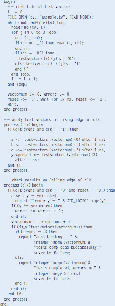
The VHDL code is rather ungainly and uses file reading commands beyond the scope of this chapter, but it gives the sense of what a self-checking testbench looks like.
New inputs are applied on the rising edge of the clock, and the output is checked on the falling edge of the clock. This clock (and reset) would also be provided to the DUT if sequential logic were being tested. Errors are reported as they occur. At the end of the simulation, the testbench prints the total number of test vectors applied and the number of errors detected.
The testbench in HDL Example 4.39 is overkill for such a simple circuit. However, it can easily be modified to test more complex circuits by changing the example.tv file, instantiating the new DUT, and changing a few lines of code to set the inputs and check the outputs.
4.9 SUMMARY
Hardware description languages (HDLs) are extremely important tools for modern digital designers. Once you have learned Verilog or VHDL, you will be able to specify digital systems much faster than if you had to draw the complete schematics. The debug cycle is also often much faster, because modifications require code changes instead of tedious schematic rewiring. However, the debug cycle can be much longer using HDLs if you don’t have a good idea of the hardware your code implies.
HDLs are used for both simulation and synthesis. Logic simulation is a powerful way to test a system on a computer before it is turned into hardware. Simulators let you check the values of signals inside your system that might be impossible to measure on a physical piece of hardware. Logic synthesis converts the HDL code into digital logic circuits.
The most important thing to remember when you are writing HDL code is that you are describing real hardware, not writing a computer program. The most common beginner’s mistake is to write HDL code without thinking about the hardware you intend to produce. If you don’t know what hardware you are implying, you are almost certain not to get what you want. Instead, begin by sketching a block diagram of your system, identifying which portions are combinational logic, which portions are sequential circuits or finite state machines, and so forth. Then write HDL code for each portion, using the correct idioms to imply the kind of hardware you need.
Exercises
The following exercises may be done using your favorite HDL. If you have a simulator available, test your design. Print the waveforms and explain how they prove that it works. If you have a synthesizer available, synthesize your code. Print the generated circuit diagram, and explain why it matches your expectations.
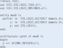
Exercise 4.1 Sketch a schematic of the circuit described by the following HDL code. Simplify the schematic so that it shows a minimum number of gates.
Verilog
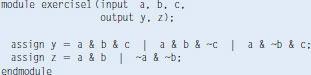
VHDL
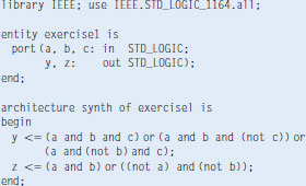
Exercise 4.2 Sketch a schematic of the circuit described by the following HDL code. Simplify the schematic so that it shows a minimum number of gates.
Verilog
VHDL
Exercise 4.3 Write an HDL module that computes a four-input XOR function. The input is a3:0, and the output is y.
Exercise 4.4 Write a self-checking testbench for Exercise 4.3. Create a test vector file containing all 16 test cases. Simulate the circuit and show that it works. Introduce an error in the test vector file and show that the testbench reports a mismatch.
Exercise 4.5 Write an HDL module called minority. It receives three inputs, a, b, and c. It produces one output, y, that is TRUE if at least two of the inputs are FALSE.
Exercise 4.6 Write an HDL module for a hexadecimal seven-segment display decoder. The decoder should handle the digits A, B, C, D, E, and F as well as 0–9.
Exercise 4.7 Write a self-checking testbench for Exercise 4.6. Create a test vector file containing all 16 test cases. Simulate the circuit and show that it works. Introduce an error in the test vector file and show that the testbench reports a mismatch.
Exercise 4.8 Write an 8:1 multiplexer module called mux8 with inputs s2:0, d0, d1, d2, d3, d4, d5, d6, d7, and output y.
Exercise 4.9 Write a structural module to compute the logic function, ![]() , using multiplexer logic. Use the 8:1 multiplexer from Exercise 4.8.
, using multiplexer logic. Use the 8:1 multiplexer from Exercise 4.8.
Exercise 4.10 Repeat Exercise 4.9 using a 4:1 multiplexer and as many NOT gates as you need.
Exercise 4.11 Section 4.5.4 pointed out that a synchronizer could be correctly described with blocking assignments if the assignments were given in the proper order. Think of a simple sequential circuit that cannot be correctly described with blocking assignments, regardless of order.
Exercise 4.12 Write an HDL module for an eight-input priority circuit.
Exercise 4.13 Write an HDL module for a 2:4 decoder.
Exercise 4.14 Write an HDL module for a 6:64 decoder using three instances of the 2:4 decoders from Exercise 4.13 and a bunch of three-input AND gates.
Exercise 4.15 Write HDL modules that implement the Boolean equations from Exercise 2.7.
Exercise 4.16 Write an HDL module that implements the circuit from Exercise 2.18.
Exercise 4.17 Write an HDL module that implements the logic function from Exercise 2.19. Pay careful attention to how you handle don’t cares.
Exercise 4.18 Write an HDL module that implements the functions from Exercise 2.24.
Exercise 4.19 Write an HDL module that implements the priority encoder from Exercise 2.25.
Exercise 4.20 Write an HDL module that implements the binary-to-thermometer code converter from Exercise 2.27.
Exercise 4.21 Write an HDL module implementing the days-in-month function from Question 2.2.
Exercise 4.22 Sketch the state transition diagram for the FSM described by the following HDL code.
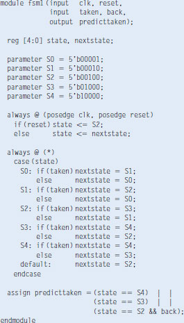
Verilog
VHDL
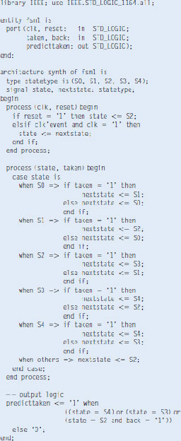
Exercise 4.23 Sketch the state transition diagram for the FSM described by the following HDL code. An FSM of this nature is used in a branch predictor on some microprocessors.
Verilog
VHDL
Exercise 4.24 Write an HDL module for an SR latch.
Exercise 4.25 Write an HDL module for a JK flip-flop. The flip-flop has inputs, clk, J, and K, and output Q. On the rising edge of the clock, Q keeps its old value if J = K = 0. It sets Q to 1 if J = 1, resets Q to 0 if K = 1, and inverts Q if J = K = 1.
Exercise 4.26 Write an HDL module for the latch from Figure 3.18. Use one assignment statement for each gate. Specify delays of 1 unit or 1 ns to each gate. Simulate the latch and show that it operates correctly. Then increase the inverter delay. How long does the delay have to be before a race condition causes the latch to malfunction?
Exercise 4.27 Write an HDL module for the traffic light controller from Section 3.4.1.
Exercise 4.28 Write three HDL modules for the factored parade mode traffic light controller from Example 3.8. The modules should be called controller, mode, and lights, and they should have the inputs and outputs shown in Figure 3.33(b).
Exercise 4.29 Write an HDL module describing the circuit in Figure 3.40.
Exercise 4.30 Write an HDL module for the FSM with the state transition diagram given in Figure 3.65 from Exercise 3.19.
Exercise 4.31 Write an HDL module for the FSM with the state transition diagram given in Figure 3.66 from Exercise 3.20.
Exercise 4.32 Write an HDL module for the improved traffic light controller from Exercise 3.21.
Exercise 4.33 Write an HDL module for the daughter snail from Exercise 3.22.
Exercise 4.34 Write an HDL module for the soda machine dispenser from Exercise 3.23.
Exercise 4.35 Write an HDL module for the Gray code counter from Exercise 3.24.
Exercise 4.36 Write an HDL module for the UP/DOWN Gray code counter from Exercise 3.25.
Exercise 4.37 Write an HDL module for the FSM from Exercise 3.26.
Exercise 4.38 Write an HDL module for the FSM from Exercise 3.27.
Exercise 4.39 Write an HDL module for the serial two’s complementer from Question 3.2.
Exercise 4.40 Write an HDL module for the circuit in Exercise 3.28.
Exercise 4.41 Write an HDL module for the circuit in Exercise 3.29.
Exercise 4.42 Write an HDL module for the circuit in Exercise 3.30.
Exercise 4.43 Write an HDL module for the circuit in Exercise 3.31. You may use the full adder from Section 4.2.5.
Verilog Exercises
The following exercises are specific to Verilog.
Exercise 4.44 What does it mean for a signal to be declared reg in Verilog?
Exercise 4.45 Rewrite the syncbad module from HDL Example 4.30. Use nonblocking assignments, but change the code to produce a correct synchronizer with two flip-flops.
Exercise 4.46 Consider the following two Verilog modules. Do they have the same function? Sketch the hardware each one implies.
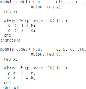
Exercise 4.47 Repeat Exercise 4.46 if the <= is replaced by = in every assignment.
Exercise 4.48 The following Verilog modules show errors that the authors have seen students make in the laboratory. Explain the error in each module and show how to fix it.
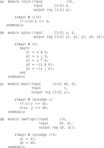
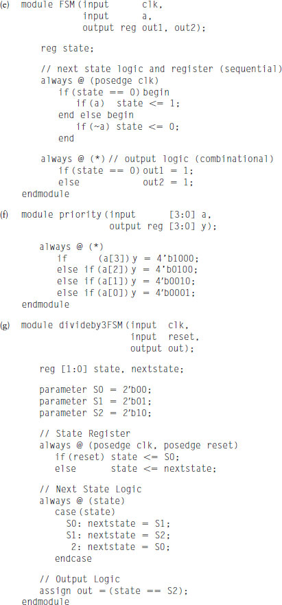
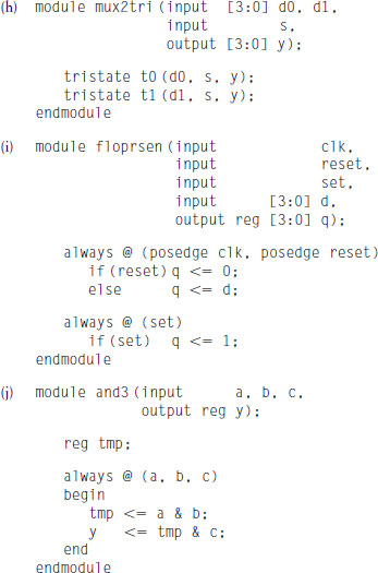
VHDL Exercises
The following exercises are specific to VHDL.
Exercise 4.49 In VHDL, why is it necessary to write
rather than simply
Exercise 4.50 Each of the following VHDL modules contains an error. For brevity, only the architecture is shown; assume that the library use clause and entity declaration are correct. Explain the error and show how to fix it.

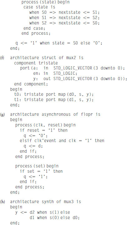
Interview Questions
The following exercises present questions that have been asked at interviews for digital design jobs.
Question 4.1 Write a line of HDL code that gates a 32-bit bus called data with another signal called sel to produce a 32-bit result. If sel is TRUE, result = data. Otherwise, result should be all 0’s.
Question 4.2 Explain the difference between blocking and nonblocking assignments in Verilog. Give examples.
Question 4.3 What does the following Verilog statement do?
1 The Institute of Electrical and Electronics Engineers (IEEE) is a professional society responsible for many computing standards including WiFi (802.11), Ethernet (802.3), and floating-point numbers (754) (see Chapter 5).
2 The simulation was performed with the Xilinx ISE Simulator, which is part of the Xilinx ISE 8.2 software. The simulator was selected because it is used commercially, yet is freely available to universities.
3 Synthesis was performed with Synplify Pro from Synplicity. The tool was selected because it is the leading commercial tool for synthesizing HDL to field-programmable gate arrays (see Section 5.6.2) and because it is available inexpensively for universities.