2 Memory Hierarchy Design
Ideally one would desire an indefinitely large memory capacity such that any particular … word would be immediately available. … We are … forced to recognize the possibility of constructing a hierarchy of memories, each of which has greater capacity than the preceding but which is less quickly accessible.
A. W. Burks, H. H. Goldstine, and J. von Neumann
Preliminary Discussion of the Logical Design of an Electronic Computing Instrument (1946)
2.1 Introduction
Computer pioneers correctly predicted that programmers would want unlimited amounts of fast memory. An economical solution to that desire is a memory hierarchy, which takes advantage of locality and trade-offs in the cost-performance of memory technologies. The principle of locality, presented in the first chapter, says that most programs do not access all code or data uniformly. Locality occurs in time (temporal locality) and in space (spatial locality). This principle, plus the guideline that for a given implementation technology and power budget smaller hardware can be made faster, led to hierarchies based on memories of different speeds and sizes. Figure 2.1 shows a multilevel memory hierarchy, including typical sizes and speeds of access.

Figure 2.1 The levels in a typical memory hierarchy in a server computer shown on top (a) and in a personal mobile device (PMD) on the bottom (b). As we move farther away from the processor, the memory in the level below becomes slower and larger. Note that the time units change by a factor of 109—from picoseconds to milliseconds—and that the size units change by a factor of 1012—from bytes to terabytes. The PMD has a slower clock rate and smaller caches and main memory. A key difference is that servers and desktops use disk storage as the lowest level in the hierarchy while PMDs use Flash, which is built from EEPROM technology.
Since fast memory is expensive, a memory hierarchy is organized into several levels—each smaller, faster, and more expensive per byte than the next lower level, which is farther from the processor. The goal is to provide a memory system with cost per byte almost as low as the cheapest level of memory and speed almost as fast as the fastest level. In most cases (but not all), the data contained in a lower level are a superset of the next higher level. This property, called the inclusion property, is always required for the lowest level of the hierarchy, which consists of main memory in the case of caches and disk memory in the case of virtual memory.
The importance of the memory hierarchy has increased with advances in performance of processors. Figure 2.2 plots single processor performance projections against the historical performance improvement in time to access main memory. The processor line shows the increase in memory requests per second on average (i.e., the inverse of the latency between memory references), while the memory line shows the increase in DRAM accesses per second (i.e., the inverse of the DRAM access latency). The situation in a uniprocessor is actually somewhat worse, since the peak memory access rate is faster than the average rate, which is what is plotted.

Figure 2.2 Starting with 1980 performance as a baseline, the gap in performance, measured as the difference in the time between processor memory requests (for a single processor or core) and the latency of a DRAM access, is plotted over time. Note that the vertical axis must be on a logarithmic scale to record the size of the processor–DRAM performance gap. The memory baseline is 64 KB DRAM in 1980, with a 1.07 per year performance improvement in latency (see Figure 2.13 on page 99). The processor line assumes a 1.25 improvement per year until 1986, a 1.52 improvement until 2000, a 1.20 improvement between 2000 and 2005, and no change in processor performance (on a per-core basis) between 2005 and 2010; see Figure 1.1 in Chapter 1.
More recently, high-end processors have moved to multiple cores, further increasing the bandwidth requirements versus single cores. In fact, the aggregate peak bandwidth essentially grows as the numbers of cores grows. A modern high-end processor such as the Intel Core i7 can generate two data memory references per core each clock cycle; with four cores and a 3.2 GHz clock rate, the i7 can generate a peak of 25.6 billion 64-bit data memory references per second, in addition to a peak instruction demand of about 12.8 billion 128-bit instruction references; this is a total peak bandwidth of 409.6 GB/sec! This incredible bandwidth is achieved by multiporting and pipelining the caches; by the use of multiple levels of caches, using separate first- and sometimes second-level caches per core; and by using a separate instruction and data cache at the first level. In contrast, the peak bandwidth to DRAM main memory is only 6% of this (25 GB/sec).
Traditionally, designers of memory hierarchies focused on optimizing average memory access time, which is determined by the cache access time, miss rate, and miss penalty. More recently, however, power has become a major consideration. In high-end microprocessors, there may be 10 MB or more of on-chip cache, and a large second- or third-level cache will consume significant power both as leakage when not operating (called static power) and as active power, as when performing a read or write (called dynamic power), as described in Section 2.3. The problem is even more acute in processors in PMDs where the CPU is less aggressive and the power budget may be 20 to 50 times smaller. In such cases, the caches can account for 25% to 50% of the total power consumption. Thus, more designs must consider both performance and power trade-offs, and we will examine both in this chapter.
Basics of Memory Hierarchies: A Quick Review
The increasing size and thus importance of this gap led to the migration of the basics of memory hierarchy into undergraduate courses in computer architecture, and even to courses in operating systems and compilers. Thus, we’ll start with a quick review of caches and their operation. The bulk of the chapter, however, describes more advanced innovations that attack the processor–memory performance gap.
When a word is not found in the cache, the word must be fetched from a lower level in the hierarchy (which may be another cache or the main memory) and placed in the cache before continuing. Multiple words, called a block (or line), are moved for efficiency reasons, and because they are likely to be needed soon due to spatial locality. Each cache block includes a tag to indicate which memory address it corresponds to.
A key design decision is where blocks (or lines) can be placed in a cache. The most popular scheme is set associative, where a set is a group of blocks in the cache. A block is first mapped onto a set, and then the block can be placed anywhere within that set. Finding a block consists of first mapping the block address to the set and then searching the set—usually in parallel—to find the block. The set is chosen by the address of the data:
If there are n blocks in a set, the cache placement is called n-way set associative. The end points of set associativity have their own names. A direct-mapped cache has just one block per set (so a block is always placed in the same location), and a fully associative cache has just one set (so a block can be placed anywhere).
Caching data that is only read is easy, since the copy in the cache and memory will be identical. Caching writes is more difficult; for example, how can the copy in the cache and memory be kept consistent? There are two main strategies. A write-through cache updates the item in the cache and writes through to update main memory. A write-back cache only updates the copy in the cache. When the block is about to be replaced, it is copied back to memory. Both write strategies can use a write buffer to allow the cache to proceed as soon as the data are placed in the buffer rather than wait the full latency to write the data into memory.
One measure of the benefits of different cache organizations is miss rate. Miss rate is simply the fraction of cache accesses that result in a miss—that is, the number of accesses that miss divided by the number of accesses.
To gain insights into the causes of high miss rates, which can inspire better cache designs, the three Cs model sorts all misses into three simple categories:
Figures B.8 and B.9 on pages B-24 and B-25 show the relative frequency of cache misses broken down by the three Cs. As we will see in Chapters 3 and 5, multithreading and multiple cores add complications for caches, both increasing the potential for capacity misses as well as adding a fourth C, for coherency misses due to cache flushes to keep multiple caches coherent in a multiprocessor; we will consider these issues in Chapter 5.
Alas, miss rate can be a misleading measure for several reasons. Hence, some designers prefer measuring misses per instruction rather than misses per memory reference (miss rate). These two are related:
(It is often reported as misses per 1000 instructions to use integers instead of fractions.)
The problem with both measures is that they don’t factor in the cost of a miss. A better measure is the average memory access time:
where hit time is the time to hit in the cache and miss penalty is the time to replace the block from memory (that is, the cost of a miss). Average memory access time is still an indirect measure of performance; although it is a better measure than miss rate, it is not a substitute for execution time. In Chapter 3 we will see that speculative processors may execute other instructions during a miss, thereby reducing the effective miss penalty. The use of multithreading (introduced in Chapter 3) also allows a processor to tolerate missses without being forced to idle. As we will examine shortly, to take advantage of such latency tolerating techniques we need caches that can service requests while handling an outstanding miss.
If this material is new to you, or if this quick review moves too quickly, see Appendix B. It covers the same introductory material in more depth and includes examples of caches from real computers and quantitative evaluations of their effectiveness.
Section B.3 in Appendix B presents six basic cache optimizations, which we quickly review here. The appendix also gives quantitative examples of the benefits of these optimizations. We also comment briefly on the power implications of these trade-offs.

Figure 2.3 Access times generally increase as cache size and associativity are increased. These data come from the CACTI model 6.5 by Tarjan, Thoziyoor, and Jouppi [2005]. The data assume a 40 nm feature size (which is between the technology used in Intel’s fastest and second fastest versions of the i7 and the same as the technology used in the fastest ARM embedded processors), a single bank, and 64-byte blocks. The assumptions about cache layout and the complex trade-offs between interconnect delays (that depend on the size of a cache block being accessed) and the cost of tag checks and multiplexing lead to results that are occasionally surprising, such as the lower access time for a 64 KB with two-way set associativity versus direct mapping. Similarly, the results with eight-way set associativity generate unusual behavior as cache size is increased. Since such observations are highly dependent on technology and detailed design assumptions, tools such as CACTI serve to reduce the search space rather than precision analysis of the trade-offs.
Note that each of the six optimizations above has a potential disadvantage that can lead to increased, rather than decreased, average memory access time.
The rest of this chapter assumes familiarity with the material above and the details in Appendix B. In the Putting It All Together section, we examine the memory hierarchy for a microprocessor designed for a high-end server, the Intel Core i7, as well as one designed for use in a PMD, the Arm Cortex-A8, which is the basis for the processor used in the Apple iPad and several high-end smartphones. Within each of these classes, there is a significant diversity in approach due to the intended use of the computer. While the high-end processor used in the server has more cores and bigger caches than the Intel processors designed for desktop uses, the processors have similar architectures. The differences are driven by performance and the nature of the workload; desktop computers are primarily running one application at a time on top of an operating system for a single user, whereas server computers may have hundreds of users running potentially dozens of applications simultaneously. Because of these workload differences, desktop computers are generally concerned more with average latency from the memory hierarchy, whereas server computers are also concerned about memory bandwidth. Even within the class of desktop computers there is wide diversity from lower end netbooks with scaled-down processors more similar to those found in high-end PMDs, to high-end desktops whose processors contain multiple cores and whose organization resembles that of a low-end server.
In contrast, PMDs not only serve one user but generally also have smaller operating systems, usually less multitasking (running of several applications simultaneously), and simpler applications. PMDs also typically use Flash memory rather than disks, and most consider both performance and energy consumption, which determines battery life.
2.2 Ten Advanced Optimizations of Cache Performance
The average memory access time formula above gives us three metrics for cache optimizations: hit time, miss rate, and miss penalty. Given the recent trends, we add cache bandwidth and power consumption to this list. We can classify the ten advanced cache optimizations we examine into five categories based on these metrics:
In general, the hardware complexity increases as we go through these optimizations. In addition, several of the optimizations require sophisticated compiler technology. We will conclude with a summary of the implementation complexity and the performance benefits of the ten techniques presented in Figure 2.11 on page 96. Since some of these are straightforward, we cover them briefly; others require more description.
First Optimization: Small and Simple First-Level Caches to Reduce Hit Time and Power
The pressure of both a fast clock cycle and power limitations encourages limited size for first-level caches. Similarly, use of lower levels of associativity can reduce both hit time and power, although such trade-offs are more complex than those involving size.
The critical timing path in a cache hit is the three-step process of addressing the tag memory using the index portion of the address, comparing the read tag value to the address, and setting the multiplexor to choose the correct data item if the cache is set associative. Direct-mapped caches can overlap the tag check with the transmission of the data, effectively reducing hit time. Furthermore, lower levels of associativity will usually reduce power because fewer cache lines must be accessed.
Although the total amount of on-chip cache has increased dramatically with new generations of microprocessors, due to the clock rate impact arising from a larger L1 cache, the size of the L1 caches has recently increased either slightly or not at all. In many recent processors, designers have opted for more associativity rather than larger caches. An additional consideration in choosing the associativity is the possibility of eliminating address aliases; we discuss this shortly.
One approach to determining the impact on hit time and power consumption in advance of building a chip is to use CAD tools. CACTI is a program to estimate the access time and energy consumption of alternative cache structures on CMOS microprocessors within 10% of more detailed CAD tools. For a given minimum feature size, CACTI estimates the hit time of caches as cache size varies, associativity, number of read/write ports, and more complex parameters. Figure 2.3 shows the estimated impact on hit time as cache size and associativity are varied. Depending on cache size, for these parameters the model suggests that the hit time for direct mapped is slightly faster than two-way set associative and that two-way set associative is 1.2 times faster than four-way and four-way is 1.4 times faster than eight-way. Of course, these estimates depend on technology as well as the size of the cache.
Example
Using the data in Figure B.8 in Appendix B and Figure 2.3, determine whether a 32 KB four-way set associative L1 cache has a faster memory access time than a 32 KB two-way set associative L1 cache. Assume the miss penalty to L2 is 15 times the access time for the faster L1 cache. Ignore misses beyond L2. Which has the faster average memory access time?
Answer
Let the access time for the two-way set associative cache be 1. Then, for the two-way cache:
For the four-way cache, the access time is 1.4 times longer. The elapsed time of the miss penalty is 15/1.4 = 10.1. Assume 10 for simplicity:
Clearly, the higher associativity looks like a bad trade-off; however, since cache access in modern processors is often pipelined, the exact impact on the clock cycle time is difficult to assess.
Energy consumption is also a consideration in choosing both the cache size and associativity, as Figure 2.4 shows. The energy cost of higher associativity ranges from more than a factor of 2 to negligible in caches of 128 KB or 256 KB when going from direct mapped to two-way set associative.

Figure 2.4 Energy consumption per read increases as cache size and associativity are increased. As in the previous figure, CACTI is used for the modeling with the same technology parameters. The large penalty for eight-way set associative caches is due to the cost of reading out eight tags and the corresponding data in parallel.
In recent designs, there are three other factors that have led to the use of higher associativity in first-level caches. First, many processors take at least two clock cycles to access the cache and thus the impact of a longer hit time may not be critical. Second, to keep the TLB out of the critical path (a delay that would be larger than that associated with increased associativity), almost all L1 caches should be virtually indexed. This limits the size of the cache to the page size times the associativity, because then only the bits within the page are used for the index. There are other solutions to the problem of indexing the cache before address translation is completed, but increasing the associativity, which also has other benefits, is the most attractive. Third, with the introduction of multithreading (see Chapter 3), conflict misses can increase, making higher associativity more attractive.
Second Optimization: Way Prediction to Reduce Hit Time
Another approach reduces conflict misses and yet maintains the hit speed of direct-mapped cache. In way prediction, extra bits are kept in the cache to predict the way, or block within the set of the next cache access. This prediction means the multiplexor is set early to select the desired block, and only a single tag comparison is performed that clock cycle in parallel with reading the cache data. A miss results in checking the other blocks for matches in the next clock cycle.
Added to each block of a cache are block predictor bits. The bits select which of the blocks to try on the next cache access. If the predictor is correct, the cache access latency is the fast hit time. If not, it tries the other block, changes the way predictor, and has a latency of one extra clock cycle. Simulations suggest that set prediction accuracy is in excess of 90% for a two-way set associative cache and 80% for a four-way set associative cache, with better accuracy on I-caches than D-caches. Way prediction yields lower average memory access time for a two-way set associative cache if it is at least 10% faster, which is quite likely. Way prediction was first used in the MIPS R10000 in the mid-1990s. It is popular in processors that use two-way set associativity and is used in the ARM Cortex-A8 with four-way set associative caches. For very fast processors, it may be challenging to implement the one cycle stall that is critical to keeping the way prediction penalty small.
An extended form of way prediction can also be used to reduce power consumption by using the way prediction bits to decide which cache block to actually access (the way prediction bits are essentially extra address bits); this approach, which might be called way selection, saves power when the way prediction is correct but adds significant time on a way misprediction, since the access, not just the tag match and selection, must be repeated. Such an optimization is likely to make sense only in low-power processors. Inoue, Ishihara, and Murakami [1999] estimated that using the way selection approach with a four-way set associative cache increases the average access time for the I-cache by 1.04 and for the D-cache by 1.13 on the SPEC95 benchmarks, but it yields an average cache power consumption relative to a normal four-way set associative cache that is 0.28 for the I-cache and 0.35 for the D-cache. One significant drawback for way selection is that it makes it difficult to pipeline the cache access.
Example
Assume that there are half as many D-cache accesses as I-cache accesses, and that the I-cache and D-cache are responsible for 25% and 15% of the processor’s power consumption in a normal four-way set associative implementation. Determine if way selection improves performance per watt based on the estimates from the study above.
Answer
For the I-cache, the savings in power is 25 × 0.28 = 0.07 of the total power, while for the D-cache it is 15 × 0.35 = 0.05 for a total savings of 0.12. The way prediction version requires 0.88 of the power requirement of the standard 4-way cache. The increase in cache access time is the increase in I-cache average access time plus one-half the increase in D-cache access time, or 1.04 + 0.5 × 0.13 = 1.11 times longer. This result means that way selection has 0.90 of the performance of a standard four-way cache. Thus, way selection improves performance per joule very slightly by a ratio of 0.90/0.88 = 1.02. This optimization is best used where power rather than performance is the key objective.
Third Optimization: Pipelined Cache Access to Increase Cache Bandwidth
This optimization is simply to pipeline cache access so that the effective latency of a first-level cache hit can be multiple clock cycles, giving fast clock cycle time and high bandwidth but slow hits. For example, the pipeline for the instruction cache access for Intel Pentium processors in the mid-1990s took 1 clock cycle, for the Pentium Pro through Pentium III in the mid-1990s through 2000 it took 2 clocks, and for the Pentium 4, which became available in 2000, and the current Intel Core i7 it takes 4 clocks. This change increases the number of pipeline stages, leading to a greater penalty on mispredicted branches and more clock cycles between issuing the load and using the data (see Chapter 3), but it does make it easier to incorporate high degrees of associativity.
Fourth Optimization: Nonblocking Caches to Increase Cache Bandwidth
For pipelined computers that allow out-of-order execution (discussed in Chapter 3), the processor need not stall on a data cache miss. For example, the processor could continue fetching instructions from the instruction cache while waiting for the data cache to return the missing data. A nonblocking cache or lockup-free cache escalates the potential benefits of such a scheme by allowing the data cache to continue to supply cache hits during a miss. This “ hit under miss” optimization reduces the effective miss penalty by being helpful during a miss instead of ignoring the requests of the processor. A subtle and complex option is that the cache may further lower the effective miss penalty if it can overlap multiple misses: a “ hit under multiple miss” or “miss under miss” optimization. The second option is beneficial only if the memory system can service multiple misses; most high-performance processors (such as the Intel Core i7) usually support both, while lower end processors, such as the ARM A8, provide only limited nonblocking support in L2.
To examine the effectiveness of nonblocking caches in reducing the cache miss penalty, Farkas and Jouppi [1994] did a study assuming 8 KB caches with a 14-cycle miss penalty; they observed a reduction in the effective miss penalty of 20% for the SPECINT92 benchmarks and 30% for the SPECFP92 benchmarks when allowing one hit under miss.
Li, Chen, Brockman, and Jouppi [2011] recently updated this study to use a multilevel cache, more modern assumptions about miss penalties, and the larger and more demanding SPEC2006 benchmarks. The study was done assuming a model based on a single core of an Intel i7 (see Section 2.6) running the SPEC2006 benchmarks. Figure 2.5 shows the reduction in data cache access latency when allowing 1, 2, and 64 hits under a miss; the caption describes further details of the memory system. The larger caches and the addition of an L3 cache since the earlier study have reduced the benefits with the SPECINT2006 benchmarks showing an average reduction in cache latency of about 9% and the SPECFP2006 benchmarks about 12.5%.

Figure 2.5 The effectiveness of a nonblocking cache is evaluated by allowing 1, 2, or 64 hits under a cache miss with 9 SPECINT (on the left) and 9 SPECFP (on the right) benchmarks. The data memory system modeled after the Intel i7 consists of a 32KB L1 cache with a four cycle access latency. The L2 cache (shared with instructions) is 256 KB with a 10 clock cycle access latency. The L3 is 2 MB and a 36-cycle access latency. All the caches are eight-way set associative and have a 64-byte block size. Allowing one hit under miss reduces the miss penalty by 9% for the integer benchmarks and 12.5% for the floating point. Allowing a second hit improves these results to 10% and 16%, and allowing 64 results in little additional improvement.
Example
Which is more important for floating-point programs: two-way set associativity or hit under one miss for the primary data caches? What about integer programs? Assume the following average miss rates for 32 KB data caches: 5.2% for floating-point programs with a direct-mapped cache, 4.9% for these programs with a two-way set associative cache, 3.5% for integer programs with a direct-mapped cache, and 3.2% for integer programs with a two-way set associative cache. Assume the miss penalty to L2 is 10 cycles, and the L2 misses and penalties are the same.
Answer
For floating-point programs, the average memory stall times are

The cache access latency (including stalls) for two-way associativity is 0.49/0.52 or 94% of direct-mapped cache. The caption of Figure 2.5 says hit under one miss reduces the average data cache access latency for floating point programs to 87.5% of a blocking cache. Hence, for floating-point programs, the direct mapped data cache supporting one hit under one miss gives better performance than a two-way set-associative cache that blocks on a miss.
For integer programs, the calculation is

The data cache access latency of a two-way set associative cache is thus 0.32/0.35 or 91% of direct-mapped cache, while the reduction in access latency when allowing a hit under one miss is 9%, making the two choices about equal.
The real difficulty with performance evaluation of nonblocking caches is that a cache miss does not necessarily stall the processor. In this case, it is difficult to judge the impact of any single miss and hence to calculate the average memory access time. The effective miss penalty is not the sum of the misses but the nonoverlapped time that the processor is stalled. The benefit of nonblocking caches is complex, as it depends upon the miss penalty when there are multiple misses, the memory reference pattern, and how many instructions the processor can execute with a miss outstanding.
In general, out-of-order processors are capable of hiding much of the miss penalty of an L1 data cache miss that hits in the L2 cache but are not capable of hiding a significant fraction of a lower level cache miss. Deciding how many outstanding misses to support depends on a variety of factors:
The following simplified example shows the key idea.
Example
Assume a main memory access time of 36 ns and a memory system capable of a sustained transfer rate of 16 GB/sec. If the block size is 64 bytes, what is the maximum number of outstanding misses we need to support assuming that we can maintain the peak bandwidth given the request stream and that accesses never conflict. If the probability of a reference colliding with one of the previous four is 50%, and we assume that the access has to wait until the earlier access completes, estimate the number of maximum outstanding references. For simplicity, ignore the time between misses.
Answer
In the first case, assuming that we can maintain the peak bandwidth, the memory system can support (16 × 10)9/64 = 250 million references per second. Since each reference takes 36 ns, we can support 250 × 106 × 36 × 10−9 = 9 references. If the probability of a collision is greater than 0, then we need more outstanding references, since we cannot start work on those references; the memory system needs more independent references not fewer! To approximate this, we can simply assume that half the memory references need not be issued to the memory. This means that we must support twice as many outstanding references, or 18.
In Li, Chen, Brockman, and Jouppi’s study they found that the reduction in CPI for the integer programs was about 7% for one hit under miss and about 12.7% for 64. For the floating point programs, the reductions were 12.7% for one hit under miss and 17.8% for 64. These reductions track fairly closely the reductions in the data cache access latency shown in Figure 2.5.
Fifth Optimization: Multibanked Caches toIncrease Cache Bandwidth
Rather than treat the cache as a single monolithic block, we can divide it into independent banks that can support simultaneous accesses. Banks were originally used to improve performance of main memory and are now used inside modern DRAM chips as well as with caches. The Arm Cortex-A8 supports one to four banks in its L2 cache; the Intel Core i7 has four banks in L1 (to support up to 2 memory accesses per clock), and the L2 has eight banks.
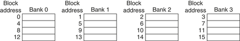
Clearly, banking works best when the accesses naturally spread themselves across the banks, so the mapping of addresses to banks affects the behavior of the memory system. A simple mapping that works well is to spread the addresses of the block sequentially across the banks, called sequential interleaving. For example, if there are four banks, bank 0 has all blocks whose address modulo 4 is 0, bank 1 has all blocks whose address modulo 4 is 1, and so on. Figure 2.6 shows this interleaving. Multiple banks also are a way to reduce power consumption both in caches and DRAM.
Sixth Optimization: Critical Word First and Early Restart to Reduce Miss Penalty
This technique is based on the observation that the processor normally needs just one word of the block at a time. This strategy is impatience: Don’t wait for the full block to be loaded before sending the requested word and restarting the processor. Here are two specific strategies:
Generally, these techniques only benefit designs with large cache blocks, since the benefit is low unless blocks are large. Note that caches normally continue to satisfy accesses to other blocks while the rest of the block is being filled.
Alas, given spatial locality, there is a good chance that the next reference is to the rest of the block. Just as with nonblocking caches, the miss penalty is not simple to calculate. When there is a second request in critical word first, the effective miss penalty is the nonoverlapped time from the reference until the second piece arrives. The benefits of critical word first and early restart depend on the size of the block and the likelihood of another access to the portion of the block that has not yet been fetched.
Seventh Optimization: Merging Write Buffer to Reduce Miss Penalty
Write-through caches rely on write buffers, as all stores must be sent to the next lower level of the hierarchy. Even write-back caches use a simple buffer when a block is replaced. If the write buffer is empty, the data and the full address are written in the buffer, and the write is finished from the processor’s perspective; the processor continues working while the write buffer prepares to write the word to memory. If the buffer contains other modified blocks, the addresses can be checked to see if the address of the new data matches the address of a valid write buffer entry. If so, the new data are combined with that entry. Write merging is the name of this optimization. The Intel Core i7, among many others, uses write merging.
If the buffer is full and there is no address match, the cache (and processor) must wait until the buffer has an empty entry. This optimization uses the memory more efficiently since multiword writes are usually faster than writes performed one word at a time. Skadron and Clark [1997] found that even a merging four-entry write buffer generated stalls that led to a 5% to 10% performance loss.
The optimization also reduces stalls due to the write buffer being full. Figure 2.7 shows a write buffer with and without write merging. Assume we had four entries in the write buffer, and each entry could hold four 64-bit words. Without this optimization, four stores to sequential addresses would fill the buffer at one word per entry, even though these four words when merged exactly fit within a single entry of the write buffer.

Figure 2.7 To illustrate write merging, the write buffer on top does not use it while the write buffer on the bottom does. The four writes are merged into a single buffer entry with write merging; without it, the buffer is full even though three-fourths of each entry is wasted. The buffer has four entries, and each entry holds four 64-bit words. The address for each entry is on the left, with a valid bit (V) indicating whether the next sequential 8 bytes in this entry are occupied. (Without write merging, the words to the right in the upper part of the figure would only be used for instructions that wrote multiple words at the same time.)
Note that input/output device registers are often mapped into the physical address space. These I/O addresses cannot allow write merging because separate I/O registers may not act like an array of words in memory. For example, they may require one address and data word per I/O register rather than use multiword writes using a single address. These side effects are typically implemented by marking the pages as requiring nonmerging write through by the caches.
Eighth Optimization: Compiler Optimizations to Reduce Miss Rate
Thus far, our techniques have required changing the hardware. This next technique reduces miss rates without any hardware changes.
This magical reduction comes from optimized software—the hardware designer’s favorite solution! The increasing performance gap between processors and main memory has inspired compiler writers to scrutinize the memory hierarchy to see if compile time optimizations can improve performance. Once again, research is split between improvements in instruction misses and improvements in data misses. The optimizations presented below are found in many modern compilers.
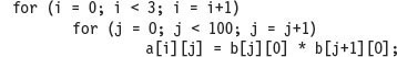
Loop Interchange
Some programs have nested loops that access data in memory in nonsequential order. Simply exchanging the nesting of the loops can make the code access the data in the order in which they are stored. Assuming the arrays do not fit in the cache, this technique reduces misses by improving spatial locality; reordering maximizes use of data in a cache block before they are discarded. For example, if x is a two-dimensional array of size [5000,100] allocated so that x[i,j] and x[i,j+1] are adjacent (an order called row major, since the array is laid out by rows), then the two pieces of code below show how the accesses can be optimized:


The original code would skip through memory in strides of 100 words, while the revised version accesses all the words in one cache block before going to the next block. This optimization improves cache performance without affecting the number of instructions executed.
Blocking
This optimization improves temporal locality to reduce misses. We are again dealing with multiple arrays, with some arrays accessed by rows and some by columns. Storing the arrays row by row (row major order) or column by column (column major order) does not solve the problem because both rows and columns are used in every loop iteration. Such orthogonal accesses mean that transformations such as loop interchange still leave plenty of room for improvement.
Instead of operating on entire rows or columns of an array, blocked algorithms operate on submatrices or blocks. The goal is to maximize accesses to the data loaded into the cache before the data are replaced. The code example below, which performs matrix multiplication, helps motivate the optimization:

The two inner loops read all N-by-N elements of z, read the same N elements in a row of y repeatedly, and write one row of N elements of x. Figure 2.8 gives a snapshot of the accesses to the three arrays. A dark shade indicates a recent access, a light shade indicates an older access, and white means not yet accessed.

Figure 2.8 A snapshot of the three arrays x, y, and z when N = 6 and i = 1. The age of accesses to the array elements is indicated by shade: white means not yet touched, light means older accesses, and dark means newer accesses. Compared to Figure 2.9, elements of y and z are read repeatedly to calculate new elements of x. The variables i, j, and k are shown along the rows or columns used to access the arrays.
The number of capacity misses clearly depends on N and the size of the cache. If it can hold all three N-by-N matrices, then all is well, provided there are no cache conflicts. If the cache can hold one N-by-N matrix and one row of N, then at least the ith row of y and the array z may stay in the cache. Less than that and misses may occur for both x and z. In the worst case, there would be 2N3 + N2 memory words accessed for N3 operations.
To ensure that the elements being accessed can fit in the cache, the original code is changed to compute on a submatrix of size B by B. Two inner loops now compute in steps of size B rather than the full length of x and z. B is called the blocking factor. (Assume x is initialized to zero.)

Figure 2.9 illustrates the accesses to the three arrays using blocking. Looking only at capacity misses, the total number of memory words accessed is 2N3/B + N2. This total is an improvement by about a factor of B. Hence, blocking exploits a combination of spatial and temporal locality, since y benefits from spatial locality and z benefits from temporal locality.

Figure 2.9 The age of accesses to the arrays x, y, and z when B = 3. Note that, in contrast to Figure 2.8, a smaller number of elements is accessed.
Although we have aimed at reducing cache misses, blocking can also be used to help register allocation. By taking a small blocking size such that the block can be held in registers, we can minimize the number of loads and stores in the program.
As we shall see in Section 4.8 of Chapter 4, cache blocking is absolutely necessary to get good performance from cache-based processors running applications using matrices as the primary data structure.
Ninth Optimization: Hardware Prefetching of Instructions and Data to Reduce Miss Penalty or Miss Rate
Nonblocking caches effectively reduce the miss penalty by overlapping execution with memory access. Another approach is to prefetch items before the processor requests them. Both instructions and data can be prefetched, either directly into the caches or into an external buffer that can be more quickly accessed than main memory.
Instruction prefetch is frequently done in hardware outside of the cache. Typically, the processor fetches two blocks on a miss: the requested block and the next consecutive block. The requested block is placed in the instruction cache when it returns, and the prefetched block is placed into the instruction stream buffer. If the requested block is present in the instruction stream buffer, the original cache request is canceled, the block is read from the stream buffer, and the next prefetch request is issued.
A similar approach can be applied to data accesses [Jouppi 1990]. Palacharla and Kessler [1994] looked at a set of scientific programs and considered multiple stream buffers that could handle either instructions or data. They found that eight stream buffers could capture 50% to 70% of all misses from a processor with two 64 KB four-way set associative caches, one for instructions and the other for data.
The Intel Core i7 supports hardware prefetching into both L1 and L2 with the most common case of prefetching being accessing the next line. Some earlier Intel processors used more aggressive hardware prefetching, but that resulted in reduced performance for some applications, causing some sophisticated users to turn off the capability.
Figure 2.10 shows the overall performance improvement for a subset of SPEC2000 programs when hardware prefetching is turned on. Note that this figure includes only 2 of 12 integer programs, while it includes the majority of the SPEC floating-point programs.

Figure 2.10 Speedup due to hardware prefetching on Intel Pentium 4 with hardware prefetching turned on for 2 of 12 SPECint2000 benchmarks and 9 of 14 SPECfp2000 benchmarks. Only the programs that benefit the most from prefetching are shown; prefetching speeds up the missing 15 SPEC benchmarks by less than 15% [Singhal 2004].
Prefetching relies on utilizing memory bandwidth that otherwise would be unused, but if it interferes with demand misses it can actually lower performance. Help from compilers can reduce useless prefetching. When prefetching works well its impact on power is negligible. When prefetched data are not used or useful data are displaced, prefetching will have a very negative impact on power.
Tenth Optimization: Compiler-Controlled Prefetching to Reduce Miss Penalty or Miss Rate
An alternative to hardware prefetching is for the compiler to insert prefetch instructions to request data before the processor needs it. There are two flavors of prefetch:
Either of these can be faulting or nonfaulting; that is, the address does or does not cause an exception for virtual address faults and protection violations. Using this terminology, a normal load instruction could be considered a “faulting register prefetch instruction.” Nonfaulting prefetches simply turn into no-ops if they would normally result in an exception, which is what we want.
The most effective prefetch is “semantically invisible” to a program: It doesn’t change the contents of registers and memory, and it cannot cause virtual memory faults. Most processors today offer nonfaulting cache prefetches. This section assumes nonfaulting cache prefetch, also called nonbinding prefetch.
Prefetching makes sense only if the processor can proceed while prefetching the data; that is, the caches do not stall but continue to supply instructions and data while waiting for the prefetched data to return. As you would expect, the data cache for such computers is normally nonblocking.
Like hardware-controlled prefetching, the goal is to overlap execution with the prefetching of data. Loops are the important targets, as they lend themselves to prefetch optimizations. If the miss penalty is small, the compiler just unrolls the loop once or twice, and it schedules the prefetches with the execution. If the miss penalty is large, it uses software pipelining (see Appendix H) or unrolls many times to prefetch data for a future iteration.
Issuing prefetch instructions incurs an instruction overhead, however, so compilers must take care to ensure that such overheads do not exceed the benefits. By concentrating on references that are likely to be cache misses, programs can avoid unnecessary prefetches while improving average memory access time significantly.
Example
For the code below, determine which accesses are likely to cause data cache misses. Next, insert prefetch instructions to reduce misses. Finally, calculate the number of prefetch instructions executed and the misses avoided by prefetching. Let’s assume we have an 8 KB direct-mapped data cache with 16-byte blocks, and it is a write-back cache that does write allocate. The elements of a and b are 8 bytes long since they are double-precision floating-point arrays. There are 3 rows and 100 columns for a and 101 rows and 3 columns for b. Let’s also assume they are not in the cache at the start of the program.
Answer
The compiler will first determine which accesses are likely to cause cache misses; otherwise, we will waste time on issuing prefetch instructions for data that would be hits. Elements of a are written in the order that they are stored in memory, so a will benefit from spatial locality: The even values of j will miss and the odd values will hit. Since a has 3 rows and 100 columns, its accesses will lead to 3 × (100/2), or 150 misses.
The array b does not benefit from spatial locality since the accesses are not in the order it is stored. The array b does benefit twice from temporal locality: The same elements are accessed for each iteration of i, and each iteration of j uses the same value of b as the last iteration. Ignoring potential conflict misses, the misses due to b will be for b[j+1][0] accesses when i = 0, and also the first access to b[j][0] when j = 0. Since j goes from 0 to 99 when i = 0, accesses to b lead to 100 + 1, or 101 misses.
Thus, this loop will miss the data cache approximately 150 times for a plus 101 times for b, or 251 misses.
To simplify our optimization, we will not worry about prefetching the first accesses of the loop. These may already be in the cache, or we will pay the miss penalty of the first few elements of a or b. Nor will we worry about suppressing the prefetches at the end of the loop that try to prefetch beyond the end of a (a[i][100] … a[i][106]) and the end of b (b[101][0] … b[107][0]). If these were faulting prefetches, we could not take this luxury. Let’s assume that the miss penalty is so large we need to start prefetching at least, say, seven iterations in advance. (Stated alternatively, we assume prefetching has no benefit until the eighth iteration.) We underline the changes to the code above needed to add prefetching.

This revised code prefetches a[i][7] through a[i][99] and b[7][0] through b[100][0], reducing the number of nonprefetched misses to
or a total of 19 nonprefetched misses. The cost of avoiding 232 cache misses is executing 400 prefetch instructions, likely a good trade-off.
Example
Calculate the time saved in the example above. Ignore instruction cache misses and assume there are no conflict or capacity misses in the data cache. Assume that prefetches can overlap with each other and with cache misses, thereby transferring at the maximum memory bandwidth. Here are the key loop times ignoring cache misses: The original loop takes 7 clock cycles per iteration, the first prefetch loop takes 9 clock cycles per iteration, and the second prefetch loop takes 8 clock cycles per iteration (including the overhead of the outer for loop). A miss takes 100 clock cycles.
Answer
The original doubly nested loop executes the multiply 3 × 100 or 300 times. Since the loop takes 7 clock cycles per iteration, the total is 300 × 7 or 2100 clock cycles plus cache misses. Cache misses add 251 × 100 or 25,100 clock cycles, giving a total of 27,200 clock cycles. The first prefetch loop iterates 100 times; at 9 clock cycles per iteration the total is 900 clock cycles plus cache misses. Now add 11 × 100 or 1100 clock cycles for cache misses, giving a total of 2000. The second loop executes 2 × 100 or 200 times, and at 8 clock cycles per iteration it takes 1600 clock cycles plus 8 × 100 or 800 clock cycles for cache misses. This gives a total of 2400 clock cycles. From the prior example, we know that this code executes 400 prefetch instructions during the 2000 + 2400 or 4400 clock cycles to execute these two loops. If we assume that the prefetches are completely overlapped with the rest of the execution, then the prefetch code is 27,200/4400, or 6.2 times faster.
Although array optimizations are easy to understand, modern programs are more likely to use pointers. Luk and Mowry [1999] have demonstrated that compiler-based prefetching can sometimes be extended to pointers as well. Of 10 programs with recursive data structures, prefetching all pointers when a node is visited improved performance by 4% to 31% in half of the programs. On the other hand, the remaining programs were still within 2% of their original performance. The issue is both whether prefetches are to data already in the cache and whether they occur early enough for the data to arrive by the time it is needed.
Many processors support instructions for cache prefetch, and high-end processors (such as the Intel Core i7) often also do some type of automated prefetch in hardware.
Cache Optimization Summary
The techniques to improve hit time, bandwidth, miss penalty, and miss rate generally affect the other components of the average memory access equation as well as the complexity of the memory hierarchy. Figure 2.11 summarizes these techniques and estimates the impact on complexity, with + meaning that the technique improves the factor, – meaning it hurts that factor, and blank meaning it has no impact. Generally, no technique helps more than one category.

Figure 2.11 Summary of 10 advanced cache optimizations showing impact on cache performance, power consumption, and complexity. Although generally a technique helps only one factor, prefetching can reduce misses if done sufficiently early; if not, it can reduce miss penalty. + means that the technique improves the factor, − means it hurts that factor, and blank means it has no impact. The complexity measure is subjective, with 0 being the easiest and 3 being a challenge.
2.3 Memory Technology and Optimizations
… the one single development that put computers on their feet was the invention of a reliable form of memory, namely, the core memory. … Its cost was reasonable, it was reliable and, because it was reliable, it could in due course be made large. [p. 209]
Main memory is the next level down in the hierarchy. Main memory satisfies the demands of caches and serves as the I/O interface, as it is the destination of input as well as the source for output. Performance measures of main memory emphasize both latency and bandwidth. Traditionally, main memory latency (which affects the cache miss penalty) is the primary concern of the cache, while main memory bandwidth is the primary concern of multiprocessors and I/O.
Although caches benefit from low-latency memory, it is generally easier to improve memory bandwidth with new organizations than it is to reduce latency. The popularity of multilevel caches and their larger block sizes make main memory bandwidth important to caches as well. In fact, cache designers increase block size to take advantage of the high memory bandwidth.
The previous sections describe what can be done with cache organization to reduce this processor–DRAM performance gap, but simply making caches larger or adding more levels of caches cannot eliminate the gap. Innovations in main memory are needed as well.
In the past, the innovation was how to organize the many DRAM chips that made up the main memory, such as multiple memory banks. Higher bandwidth is available using memory banks, by making memory and its bus wider, or by doing both. Ironically, as capacity per memory chip increases, there are fewer chips in the same-sized memory system, reducing possibilities for wider memory systems with the same capacity.
To allow memory systems to keep up with the bandwidth demands of modern processors, memory innovations started happening inside the DRAM chips themselves. This section describes the technology inside the memory chips and those innovative, internal organizations. Before describing the technologies and options, let’s go over the performance metrics.
With the introduction of burst transfer memories, now widely used in both Flash and DRAM, memory latency is quoted using two measures— access time and cycle time. Access time is the time between when a read is requested and when the desired word arrives, and cycle time is the minimum time between unrelated requests to memory.
Virtually all computers since 1975 have used DRAMs for main memory and SRAMs for cache, with one to three levels integrated onto the processor chip with the CPU. In PMDs, the memory technology often balances power and speed, with higher end systems using fast, high-bandwidth memory technology.
SRAM Technology
The first letter of SRAM stands for static. The dynamic nature of the circuits in DRAM requires data to be written back after being read—hence the difference between the access time and the cycle time as well as the need to refresh. SRAMs don’t need to refresh, so the access time is very close to the cycle time. SRAMs typically use six transistors per bit to prevent the information from being disturbed when read. SRAM needs only minimal power to retain the charge in standby mode.
In earlier times, most desktop and server systems used SRAM chips for their primary, secondary, or tertiary caches; today, all three levels of caches are integrated onto the processor chip. Currently, the largest on-chip, third-level caches are 12 MB, while the memory system for such a processor is likely to have 4 to 16 GB of DRAM. The access times for large, third-level, on-chip caches are typically two to four times that of a second-level cache, which is still three to five times faster than accessing DRAM memory.
DRAM Technology
As early DRAMs grew in capacity, the cost of a package with all the necessary address lines was an issue. The solution was to multiplex the address lines, thereby cutting the number of address pins in half. Figure 2.12 shows the basic DRAM organization. One-half of the address is sent first during the row access strobe (RAS). The other half of the address, sent during the column access strobe (CAS), follows it. These names come from the internal chip organization, since the memory is organized as a rectangular matrix addressed by rows and columns.

Figure 2.12 Internal organization of a DRAM. Modern DRAMs are organized in banks, typically four for DDR3. Each bank consists of a series of rows. Sending a PRE (precharge) command opens or closes a bank. A row address is sent with an Act (activate), which causes the row to transfer to a buffer. When the row is in the buffer, it can be transferred by successive column addresses at whatever the width of the DRAM is (typically 4, 8, or 16 bits in DDR3) or by specifying a block transfer and the starting address. Each command, as well as block transfers, are synchronized with a clock.
An additional requirement of DRAM derives from the property signified by its first letter, D, for dynamic. To pack more bits per chip, DRAMs use only a single transistor to store a bit. Reading that bit destroys the information, so it must be restored. This is one reason why the DRAM cycle time was traditionally longer than the access time; more recently, DRAMs have introduced multiple banks, which allow the rewrite portion of the cycle to be hidden. In addition, to prevent loss of information when a bit is not read or written, the bit must be “refreshed” periodically. Fortunately, all the bits in a row can be refreshed simultaneously just by reading that row. Hence, every DRAM in the memory system must access every row within a certain time window, such as 8 ms. Memory controllers include hardware to refresh the DRAMs periodically.
This requirement means that the memory system is occasionally unavailable because it is sending a signal telling every chip to refresh. The time for a refresh is typically a full memory access (RAS and CAS) for each row of the DRAM. Since the memory matrix in a DRAM is conceptually square, the number of steps in a refresh is usually the square root of the DRAM capacity. DRAM designers try to keep time spent refreshing to less than 5% of the total time.
So far we have presented main memory as if it operated like a Swiss train, consistently delivering the goods exactly according to schedule. Refresh belies that analogy, since some accesses take much longer than others do. Thus, refresh is another reason for variability of memory latency and hence cache miss penalty.
Amdahl suggested as a rule of thumb that memory capacity should grow linearly with processor speed to keep a balanced system, so that a 1000 MIPS processor should have 1000 MB of memory. Processor designers rely on DRAMs to supply that demand. In the past, they expected a fourfold improvement in capacity every three years, or 55% per year. Unfortunately, the performance of DRAMs is growing at a much slower rate. Figure 2.13 shows a performance improvement in row access time, which is related to latency, of about 5% per year. The CAS or data transfer time, which is related to bandwidth, is growing at more than twice that rate.
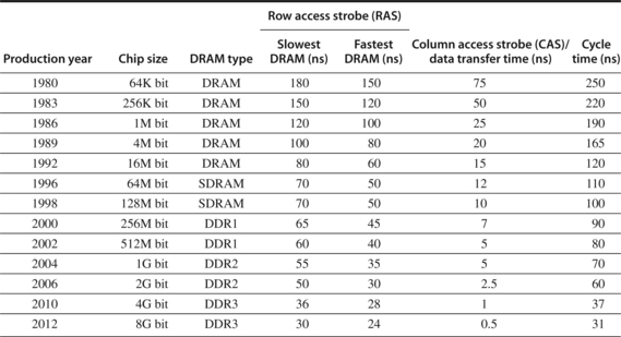
Figure 2.13 Times of fast and slow DRAMs vary with each generation. (Cycle time is defined on page 97.) Performance improvement of row access time is about 5% per year. The improvement by a factor of 2 in column access in 1986 accompanied the switch from NMOS DRAMs to CMOS DRAMs. The introduction of various burst transfer modes in the mid-1990s and SDRAMs in the late 1990s has significantly complicated the calculation of access time for blocks of data; we discuss this later in this section when we talk about SDRAM access time and power. The DDR4 designs are due for introduction in mid- to late 2012. We discuss these various forms of DRAMs in the next few pages.
Although we have been talking about individual chips, DRAMs are commonly sold on small boards called dual inline memory modules (DIMMs). DIMMs typically contain 4 to 16 DRAMs, and they are normally organized to be 8 bytes wide (+ ECC) for desktop and server systems.
In addition to the DIMM packaging and the new interfaces to improve the data transfer time, discussed in the following subsections, the biggest change to DRAMs has been a slowing down in capacity growth. DRAMs obeyed Moore’s law for 20 years, bringing out a new chip with four times the capacity every three years. Due to the manufacturing challenges of a single-bit DRAM, new chips only double capacity every two years since 1998. In 2006, the pace slowed further, with the four years from 2006 to 2010 seeing only a doubling of capacity.
Improving Memory Performance Inside a DRAM Chip
As Moore’s law continues to supply more transistors and as the processor–memory gap increases pressure on memory performance, the ideas of the previous section have made their way inside the DRAM chip. Generally, innovation has led to greater bandwidth, sometimes at the cost of greater latency. This subsection presents techniques that take advantage of the nature of DRAMs.
As mentioned earlier, a DRAM access is divided into row access and column access. DRAMs must buffer a row of bits inside the DRAM for the column access, and this row is usually the square root of the DRAM size—for example, 2 Kb for a 4 Mb DRAM. As DRAMs grew, additional structure and several opportunities for increasing bandwith were added.
First, DRAMs added timing signals that allow repeated accesses to the row buffer without another row access time. Such a buffer comes naturally, as each array will buffer 1024 to 4096 bits for each access. Initially, separate column addresses had to be sent for each transfer with a delay after each new set of column addresses.
Originally, DRAMs had an asynchronous interface to the memory controller, so every transfer involved overhead to synchronize with the controller. The second major change was to add a clock signal to the DRAM interface, so that the repeated transfers would not bear that overhead. Synchronous DRAM (SDRAM) is the name of this optimization. SDRAMs typically also have a programmable register to hold the number of bytes requested, and hence can send many bytes over several cycles per request. Typically, 8 or more 16-bit transfers can occur without sending any new addresses by placing the DRAM in burst mode; this mode, which supports critical word first transfers, is the only way that the peak bandwidths shown in Figure 2.14 can be achieved.
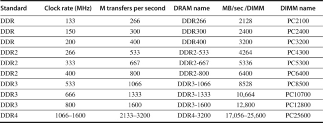
Figure 2.14 Clock rates, bandwidth, and names of DDR DRAMS and DIMMs in 2010. Note the numerical relationship between the columns. The third column is twice the second, and the fourth uses the number from the third column in the name of the DRAM chip. The fifth column is eight times the third column, and a rounded version of this number is used in the name of the DIMM. Although not shown in this figure, DDRs also specify latency in clock cycles as four numbers, which are specified by the DDR standard. For example, DDR3-2000 CL 9 has latencies of 9-9-9-28. What does this mean? With a 1 ns clock (clock cycle is one-half the transfer rate), this indicates 9 ns for row to columns address (RAS time), 9 ns for column access to data (CAS time), and a minimum read time of 28 ns. Closing the row takes 9 ns for precharge but happens only when the reads from that row are finished. In burst mode, transfers occur on every clock on both edges, when the first RAS and CAS times have elapsed. Furthermore, the precharge is not needed until the entire row is read. DDR4 will be produced in 2012 and is expected to reach clock rates of 1600 MHz in 2014, when DDR5 is expected to take over. The exercises explore these details further.
Third, to overcome the problem of getting a wide stream of bits from the memory without having to make the memory system too large as memory system density increased, DRAMS were made wider. Initially, they offered a four-bit transfer mode; in 2010, DDR2 and DDR3 DRAMS had up to 16-bit buses.
The fourth major DRAM innovation to increase bandwidth is to transfer data on both the rising edge and falling edge of the DRAM clock signal, thereby doubling the peak data rate. This optimization is called double data rate (DDR).
To provide some of the advantages of interleaving, as well to help with power management, SDRAMs also introduced banks, breaking a single SDRAM into 2 to 8 blocks (in current DDR3 DRAMs) that can operate independently. (We have already seen banks used in internal caches, and they were often used in large main memories.) Creating multiple banks inside a DRAM effectively adds another segment to the address, which now consists of bank number, row address, and column address. When an address is sent that designates a new bank, that bank must be opened, incurring an additional delay. The management of banks and row buffers is completely handled by modern memory control interfaces, so that when subsequent access specifies the same row for an open bank, the access can happen quickly, sending only the column address.
When DDR SDRAMs are packaged as DIMMs, they are confusingly labeled by the peak DIMM bandwidth. Hence, the DIMM name PC2100 comes from 133 MHz × 2 × 8 bytes, or 2100 MB/sec. Sustaining the confusion, the chips themselves are labeled with the number of bits per second rather than their clock rate, so a 133 MHz DDR chip is called a DDR266. Figure 2.14 shows the relationships among clock rate, transfers per second per chip, chip name, DIMM bandwidth, and DIMM name.
DDR is now a sequence of standards. DDR2 lowers power by dropping the voltage from 2.5 volts to 1.8 volts and offers higher clock rates: 266 MHz, 333 MHz, and 400 MHz. DDR3 drops voltage to 1.5 volts and has a maximum clock speed of 800 MHz. DDR4, scheduled for production in 2014, drops the voltage to 1 to 1.2 volts and has a maximum expected clock rate of 1600 MHz. DDR5 will follow in about 2014 or 2015. (As we discuss in the next section, GDDR5 is a graphics RAM and is based on DDR3 DRAMs.)
Graphics Data RAMs
GDRAMs or GSDRAMs (Graphics or Graphics Synchronous DRAMs) are a special class of DRAMs based on SDRAM designs but tailored for handling the higher bandwidth demands of graphics processing units. GDDR5 is based on DDR3 with earlier GDDRs based on DDR2. Since Graphics Processor Units (GPUs; see Chapter 4) require more bandwidth per DRAM chip than CPUs, GDDRs have several important differences:
Altogether, these characteristics let GDDRs run at two to five times the bandwidth per DRAM versus DDR3 DRAMs, a significant advantage in supporting GPUs. Because of the lower locality of memory requests in a GPU, burst mode generally is less useful for a GPU, but keeping open multiple memory banks and managing their use improves effective bandwidth.
Reducing Power Consumption in SDRAMs
Power consumption in dynamic memory chips consists of both dynamic power used in a read or write and static or standby power; both depend on the operating voltage. In the most advanced DDR3 SDRAMs the operating voltage has been dropped to 1.35 to 1.5 volts, significantly reducing power versus DDR2 SDRAMs. The addition of banks also reduced power, since only the row in a single bank is read and precharged.
In addition to these changes, all recent SDRAMs support a power down mode, which is entered by telling the DRAM to ignore the clock. Power down mode disables the SDRAM, except for internal automatic refresh (without which entering power down mode for longer than the refresh time will cause the contents of memory to be lost). Figure 2.15 shows the power consumption for three situations in a 2 Gb DDR3 SDRAM. The exact delay required to return from low power mode depends on the SDRAM, but a typical timing from autorefresh low power mode is 200 clock cycles; additional time may be required for resetting the mode register before the first command.

Figure 2.15 Power consumption for a DDR3 SDRAM operating under three conditions: low power (shutdown) mode, typical system mode (DRAM is active 30% of the time for reads and 15% for writes), and fully active mode, where the DRAM is continuously reading or writing when not in precharge. Reads and writes assume bursts of 8 transfers. These data are based on a Micron 1.5V 2Gb DDR3-1066.
Flash Memory
Flash memory is a type of EEPROM (Electronically Erasable Programmable Read-Only Memory), which is normally read-only but can be erased. The other key property of Flash memory is that it holds it contents without any power.
Flash is used as the backup storage in PMDs in the same manner that a disk functions in a laptop or server. In addition, because most PMDs have a limited amount of DRAM, Flash may also act as a level of the memory hierarchy, to a much larger extent than it might have to do so in the desktop or server with a main memory that might be 10 to 100 times larger.
Flash uses a very different architecture and has different properties than standard DRAM. The most important differences are
The rapid improvements in high-density Flash in the past decade have made the technology a viable part of memory hierarchies in mobile devices and as solid-state replacements for disks. As the rate of increase in DRAM density continues to drop, Flash could play an increased role in future memory systems, acting as both a replacement for hard disks and as an intermediate storage between DRAM and disk.
Enhancing Dependability in Memory Systems
Large caches and main memories significantly increase the possibility of errors occurring both during the fabrication process and dynamically, primarily from cosmic rays striking a memory cell. These dynamic errors, which are changes to a cell’s contents, not a change in the circuitry, are called soft errors. All DRAMs, Flash memory, and many SRAMs are manufactured with spare rows, so that a small number of manufacturing defects can be accommodated by programming the replacement of a defective row by a spare row. In addition to fabrication errors that must be fixed at configuration time, hard errors, which are permanent changes in the operation of one of more memory cells, can occur in operation.
Dynamic errors can be detected by parity bits and detected and fixed by the use of Error Correcting Codes (ECCs). Because instruction caches are read-only, parity suffices. In larger data caches and in main memory, ECC is used to allow errors to be both detected and corrected. Parity requires only one bit of overhead to detect a single error in a sequence of bits. Because a multibit error would be undetected with parity, the number of bits protected by a parity bit must be limited. One parity bit per 8 data bits is a typical ratio. ECC can detect two errors and correct a single error with a cost of 8 bits of overhead per 64 data bits.
In very large systems, the possibility of multiple errors as well as complete failure of a single memory chip becomes significant. Chipkill was introduced by IBM to solve this problem, and many very large systems, such as IBM and SUN servers and the Google Clusters, use this technology. (Intel calls their version SDDC.) Similar in nature to the RAID approach used for disks, Chipkill distributes the data and ECC information, so that the complete failure of a single memory chip can be handled by supporting the reconstruction of the missing data from the remaining memory chips. Using an analysis by IBM and assuming a 10,000 processor server with 4 GB per processor yields the following rates of unrecoverable errors in three years of operation:
Another way to look at this is to find the maximum number of servers (each with 4 GB) that can be protected while achieving the same error rate as demonstrated for Chipkill. For parity, even a server with only one processor will have an unrecoverable error rate higher than a 10,000-server Chipkill protected system. For ECC, a 17-server system would have about the same failure rate as a 10,000-server Chipkill system. Hence, Chipkill is a requirement for the 50,000 to 100,00 servers in warehouse-scale computers (see Section 6.8 of Chapter 6).
2.4 Protection: Virtual Memory and Virtual Machines
A virtual machine is taken to be an efficient, isolated duplicate of the real machine. We explain these notions through the idea of a virtual machine monitor (VMM)…. a VMM has three essential characteristics. First, the VMM provides an environment for programs which is essentially identical with the original machine; second, programs run in this environment show at worst only minor decreases in speed; and last, the VMM is in complete control of system resources.
Gerald Popek and Robert Goldberg
“Formal requirements for virtualizable third generation architectures,”
Security and privacy are two of the most vexing challenges for information technology in 2011. Electronic burglaries, often involving lists of credit card numbers, are announced regularly, and it’s widely believed that many more go unreported. Hence, both researchers and practitioners are looking for new ways to make computing systems more secure. Although protecting information is not limited to hardware, in our view real security and privacy will likely involve innovation in computer architecture as well as in systems software.
This section starts with a review of the architecture support for protecting processes from each other via virtual memory. It then describes the added protection provided from virtual machines, the architecture requirements of virtual machines, and the performance of a virtual machine. As we will see in Chapter 6, virtual machines are a foundational technology for cloud computing.
Protection via Virtual Memory
Page-based virtual memory, including a translation lookaside buffer that caches page table entries, is the primary mechanism that protects processes from each other. Sections B.4 and B.5 in Appendix B review virtual memory, including a detailed description of protection via segmentation and paging in the 80x86. This subsection acts as a quick review; refer to those sections if it’s too quick.
Multiprogramming, where several programs running concurrently would share a computer, led to demands for protection and sharing among programs and to the concept of a process. Metaphorically, a process is a program’s breathing air and living space—that is, a running program plus any state needed to continue running it. At any instant, it must be possible to switch from one process to another. This exchange is called a process switch or context switch.
The operating system and architecture join forces to allow processes to share the hardware yet not interfere with each other. To do this, the architecture must limit what a process can access when running a user process yet allow an operating system process to access more. At a minimum, the architecture must do the following:
Appendix A describes several memory protection schemes, but by far the most popular is adding protection restrictions to each page of virtual memory. Fixed-sized pages, typically 4 KB or 8 KB long, are mapped from the virtual address space into physical address space via a page table. The protection restrictions are included in each page table entry. The protection restrictions might determine whether a user process can read this page, whether a user process can write to this page, and whether code can be executed from this page. In addition, a process can neither read nor write a page if it is not in the page table. Since only the OS can update the page table, the paging mechanism provides total access protection.
Paged virtual memory means that every memory access logically takes at least twice as long, with one memory access to obtain the physical address and a second access to get the data. This cost would be far too dear. The solution is to rely on the principle of locality; if the accesses have locality, then the address translations for the accesses must also have locality. By keeping these address translations in a special cache, a memory access rarely requires a second access to translate the address. This special address translation cache is referred to as a translation lookaside buffer (TLB).
A TLB entry is like a cache entry where the tag holds portions of the virtual address and the data portion holds a physical page address, protection field, valid bit, and usually a use bit and a dirty bit. The operating system changes these bits by changing the value in the page table and then invalidating the corresponding TLB entry. When the entry is reloaded from the page table, the TLB gets an accurate copy of the bits.
Assuming the computer faithfully obeys the restrictions on pages and maps virtual addresses to physical addresses, it would seem that we are done. Newspaper headlines suggest otherwise.
The reason we’re not done is that we depend on the accuracy of the operating system as well as the hardware. Today’s operating systems consist of tens of millions of lines of code. Since bugs are measured in number per thousand lines of code, there are thousands of bugs in production operating systems. Flaws in the OS have led to vulnerabilities that are routinely exploited.
This problem and the possibility that not enforcing protection could be much more costly than in the past have led some to look for a protection model with a much smaller code base than the full OS, such as Virtual Machines.
Protection via Virtual Machines
An idea related to virtual memory that is almost as old are Virtual Machines (VMs). They were first developed in the late 1960s, and they have remained an important part of mainframe computing over the years. Although largely ignored in the domain of single-user computers in the 1980s and 1990s, they have recently gained popularity due to
The broadest definition of VMs includes basically all emulation methods that provide a standard software interface, such as the Java VM. We are interested in VMs that provide a complete system-level environment at the binary instruction set architecture (ISA) level. Most often, the VM supports the same ISA as the underlying hardware; however, it is also possible to support a different ISA, and such approaches are often employed when migrating between ISAs, so as to allow software from the departing ISA to be used until it can be ported to the new ISA. Our focus here will be in VMs where the ISA presented by the VM and the underlying hardware match. Such VMs are called (Operating) System Virtual Machines. IBM VM/370, VMware ESX Server, and Xen are examples. They present the illusion that the users of a VM have an entire computer to themselves, including a copy of the operating system. A single computer runs multiple VMs and can support a number of different operating systems (OSes). On a conventional platform, a single OS “owns” all the hardware resources, but with a VM multiple OSes all share the hardware resources.
The software that supports VMs is called a virtual machine monitor (VMM) or hypervisor; the VMM is the heart of virtual machine technology. The underlying hardware platform is called the host, and its resources are shared among the guest VMs. The VMM determines how to map virtual resources to physical resources: A physical resource may be time-shared, partitioned, or even emulated in software. The VMM is much smaller than a traditional OS; the isolation portion of a VMM is perhaps only 10,000 lines of code.
In general, the cost of processor virtualization depends on the workload. User-level processor-bound programs, such as SPEC CPU2006, have zero virtualization overhead because the OS is rarely invoked so everything runs at native speeds. Conversely, I/O-intensive workloads generally are also OS-intensive and execute many system calls (which doing I/O requires) and privileged instructions that can result in high virtualization overhead. The overhead is determined by the number of instructions that must be emulated by the VMM and how slowly they are emulated. Hence, when the guest VMs run the same ISA as the host, as we assume here, the goal of the architecture and the VMM is to run almost all instructions directly on the native hardware. On the other hand, if the I/O-intensive workload is also I/O-bound, the cost of processor virtualization can be completely hidden by low processor utilization since it is often waiting for I/O.
Although our interest here is in VMs for improving protection, VMs provide two other benefits that are commercially significant:
These two reasons are why cloud-based servers, such as Amazon’s, rely on virtual machines.
Requirements of a Virtual Machine Monitor
What must a VM monitor do? It presents a software interface to guest software, it must isolate the state of guests from each other, and it must protect itself from guest software (including guest OSes). The qualitative requirements are
To “virtualize” the processor, the VMM must control just about everything—access to privileged state, address translation, I/O, exceptions and interrupts—even though the guest VM and OS currently running are temporarily using them.
For example, in the case of a timer interrupt, the VMM would suspend the currently running guest VM, save its state, handle the interrupt, determine which guest VM to run next, and then load its state. Guest VMs that rely on a timer interrupt are provided with a virtual timer and an emulated timer interrupt by the VMM.
To be in charge, the VMM must be at a higher privilege level than the guest VM, which generally runs in user mode; this also ensures that the execution of any privileged instruction will be handled by the VMM. The basic requirements of system virtual machines are almost identical to those for paged virtual memory listed above:
(Lack of) Instruction Set Architecture Support for Virtual Machines
If VMs are planned for during the design of the ISA, it’s relatively easy to both reduce the number of instructions that must be executed by a VMM and how long it takes to emulate them. An architecture that allows the VM to execute directly on the hardware earns the title virtualizable, and the IBM 370 architecture proudly bears that label.
Alas, since VMs have been considered for desktop and PC-based server applications only fairly recently, most instruction sets were created without virtualization in mind. These culprits include 80x86 and most RISC architectures.
Because the VMM must ensure that the guest system only interacts with virtual resources, a conventional guest OS runs as a user mode program on top of the VMM. Then, if a guest OS attempts to access or modify information related to hardware resources via a privileged instruction—for example, reading or writing the page table pointer—it will trap to the VMM. The VMM can then effect the appropriate changes to corresponding real resources.
Hence, if any instruction that tries to read or write such sensitive information traps when executed in user mode, the VMM can intercept it and support a virtual version of the sensitive information as the guest OS expects.
In the absence of such support, other measures must be taken. A VMM must take special precautions to locate all problematic instructions and ensure that they behave correctly when executed by a guest OS, thereby increasing the complexity of the VMM and reducing the performance of running the VM.
Sections 2.5 and 2.7 give concrete examples of problematic instructions in the 80x86 architecture.
Impact of Virtual Machines on Virtual Memory and I/O
Another challenge is virtualization of virtual memory, as each guest OS in every VM manages its own set of page tables. To make this work, the VMM separates the notions of real and physical memory (which are often treated synonymously) and makes real memory a separate, intermediate level between virtual memory and physical memory. (Some use the terms virtual memory, physical memory, and machine memory to name the same three levels.) The guest OS maps virtual memory to real memory via its page tables, and the VMM page tables map the guests’ real memory to physical memory. The virtual memory architecture is specified either via page tables, as in IBM VM/370 and the 80x86, or via the TLB structure, as in many RISC architectures.
Rather than pay an extra level of indirection on every memory access, the VMM maintains a shadow page table that maps directly from the guest virtual address space to the physical address space of the hardware. By detecting all modifications to the guest’s page table, the VMM can ensure the shadow page table entries being used by the hardware for translations correspond to those of the guest OS environment, with the exception of the correct physical pages substituted for the real pages in the guest tables. Hence, the VMM must trap any attempt by the guest OS to change its page table or to access the page table pointer. This is commonly done by write protecting the guest page tables and trapping any access to the page table pointer by a guest OS. As noted above, the latter happens naturally if accessing the page table pointer is a privileged operation.
The IBM 370 architecture solved the page table problem in the 1970s with an additional level of indirection that is managed by the VMM. The guest OS keeps its page tables as before, so the shadow pages are unnecessary. AMD has proposed a similar scheme for their Pacifica revision to the 80x86.
To virtualize the TLB in many RISC computers, the VMM manages the real TLB and has a copy of the contents of the TLB of each guest VM. To pull this off, any instructions that access the TLB must trap. TLBs with Process ID tags can support a mix of entries from different VMs and the VMM, thereby avoiding flushing of the TLB on a VM switch. Meanwhile, in the background, the VMM supports a mapping between the VMs’ virtual Process IDs and the real Process IDs.
The final portion of the architecture to virtualize is I/O. This is by far the most difficult part of system virtualization because of the increasing number of I/O devices attached to the computer and the increasing diversity of I/O device types. Another difficulty is the sharing of a real device among multiple VMs, and yet another comes from supporting the myriad of device drivers that are required, especially if different guest OSes are supported on the same VM system. The VM illusion can be maintained by giving each VM generic versions of each type of I/O device driver, and then leaving it to the VMM to handle real I/O.
The method for mapping a virtual to physical I/O device depends on the type of device. For example, physical disks are normally partitioned by the VMM to create virtual disks for guest VMs, and the VMM maintains the mapping of virtual tracks and sectors to the physical ones. Network interfaces are often shared between VMs in very short time slices, and the job of the VMM is to keep track of messages for the virtual network addresses to ensure that guest VMs receive only messages intended for them.
An Example VMM: The Xen Virtual Machine
Early in the development of VMs, a number of inefficiencies became apparent. For example, a guest OS manages its virtual to real page mapping, but this mapping is ignored by the VMM, which performs the actual mapping to physical pages. In other words, a significant amount of wasted effort is expended just to keep the guest OS happy. To reduce such inefficiencies, VMM developers decided that it may be worthwhile to allow the guest OS to be aware that it is running on a VM. For example, a guest OS could assume a real memory as large as its virtual memory so that no memory management is required by the guest OS.
Allowing small modifications to the guest OS to simplify virtualization is referred to as paravirtualization, and the open source Xen VMM is a good example. The Xen VMM, which is used in Amazon’s Web services data centers, provides a guest OS with a virtual machine abstraction that is similar to the physical hardware, but it drops many of the troublesome pieces. For example, to avoid flushing the TLB, Xen maps itself into the upper 64 MB of the address space of each VM. It allows the guest OS to allocate pages, just checking to be sure it does not violate protection restrictions. To protect the guest OS from the user programs in the VM, Xen takes advantage of the four protection levels available in the 80x86. The Xen VMM runs at the highest privilege level (0), the guest OS runs at the next level (1), and the applications run at the lowest privilege level (3). Most OSes for the 80x86 keep everything at privilege levels 0 or 3.
For subsetting to work properly, Xen modifies the guest OS to not use problematic portions of the architecture. For example, the port of Linux to Xen changes about 3000 lines, or about 1% of the 80x86-specific code. These changes, however, do not affect the application-binary interfaces of the guest OS.
To simplify the I/O challenge of VMs, Xen assigned privileged virtual machines to each hardware I/O device. These special VMs are called driver domains. (Xen calls its VMs “domains.”) Driver domains run the physical device drivers, although interrupts are still handled by the VMM before being sent to the appropriate driver domain. Regular VMs, called guest domains, run simple virtual device drivers that must communicate with the physical device drivers in the driver domains over a channel to access the physical I/O hardware. Data are sent between guest and driver domains by page remapping.
2.5 Crosscutting Issues: The Design of Memory Hierarchies
This section describes three topics discussed in other chapters that are fundamental to memory hierarchies.
Protection and Instruction Set Architecture
Protection is a joint effort of architecture and operating systems, but architects had to modify some awkward details of existing instruction set architectures when virtual memory became popular. For example, to support virtual memory in the IBM 370, architects had to change the successful IBM 360 instruction set architecture that had been announced just 6 years before. Similar adjustments are being made today to accommodate virtual machines.
For example, the 80x86 instruction POPF loads the flag registers from the top of the stack in memory. One of the flags is the Interrupt Enable (IE) flag. Until recent changes to support virtualization, running the POPF instruction in user mode, rather than trapping it, simply changed all the flags except IE. In system mode, it does change the IE flag. Since a guest OS runs in user mode inside a VM, this was a problem, as it would expect to see a changed IE. Extensions of the 80x86 architecture to support virtualization eliminated this problem.
Historically, IBM mainframe hardware and VMM took three steps to improve performance of virtual machines:
IBM is still the gold standard of virtual machine technology. For example, an IBM mainframe ran thousands of Linux VMs in 2000, while Xen ran 25 VMs in 2004 [Clark et al. 2004]. Recent versions of Intel and AMD chipsets have added special instructions to support devices in a VM, to mask interrupts at lower levels from each VM, and to steer interrupts to the appropriate VM.
Coherency of Cached Data
Data can be found in memory and in the cache. As long as the processor is the sole component changing or reading the data and the cache stands between the processor and memory, there is little danger in the processor seeing the old or stale copy. As we will see, multiple processors and I/O devices raise the opportunity for copies to be inconsistent and to read the wrong copy.
The frequency of the cache coherency problem is different for multiprocessors than I/O. Multiple data copies are a rare event for I/O—one to be avoided whenever possible—but a program running on multiple processors will want to have copies of the same data in several caches. Performance of a multiprocessor program depends on the performance of the system when sharing data.
The I/O cache coherency question is this: Where does the I/O occur in the computer—between the I/O device and the cache or between the I/O device and main memory? If input puts data into the cache and output reads data from the cache, both I/O and the processor see the same data. The difficulty in this approach is that it interferes with the processor and can cause the processor to stall for I/O. Input may also interfere with the cache by displacing some information with new data that are unlikely to be accessed soon.
The goal for the I/O system in a computer with a cache is to prevent the stale data problem while interfering as little as possible. Many systems, therefore, prefer that I/O occur directly to main memory, with main memory acting as an I/O buffer. If a write-through cache were used, then memory would have an up-to-date copy of the information, and there would be no stale data issue for output. (This benefit is a reason processors used write through.) Alas, write through is usually found today only in first-level data caches backed by an L2 cache that uses write back.
Input requires some extra work. The software solution is to guarantee that no blocks of the input buffer are in the cache. A page containing the buffer can be marked as noncacheable, and the operating system can always input to such a page. Alternatively, the operating system can flush the buffer addresses from the cache before the input occurs. A hardware solution is to check the I/O addresses on input to see if they are in the cache. If there is a match of I/O addresses in the cache, the cache entries are invalidated to avoid stale data. All of these approaches can also be used for output with write-back caches.
Processor cache coherency is a critical subject in the age of multicore processors, and we will examine it in detail in Chapter 5.
2.6 Putting It All Together: Memory Hierachies in the ARM Cortex-A8 and Intel Core i7
This section reveals the ARM Cortex-A8 (hereafter called the Cortex-A8) and Intel Core i7 (hereafter called i7) memory hierarchies and shows the performance of their components on a set of single threaded benchmarks. We examine the Cortex-A8 first because it has a simpler memory system; we go into more detail for the i7, tracing out a memory reference in detail. This section presumes that readers are familiar with the organization of a two-level cache hierarchy using virtually indexed caches. The basics of such a memory system are explained in detail in Appendix B, and readers who are uncertain of the organization of such a system are strongly advised to review the Opteron example in Appendix B. Once they understand the organization of the Opteron, the brief explanation of the Cortex-A8 system, which is similar, will be easy to follow.
The ARM Cortex-A8
The Cortex-A8 is a configurable core that supports the ARMv7 instruction set architecture. It is delivered as an IP (Intellectual Property) core. IP cores are the dominant form of technology delivery in the embedded, PMD, and related markets; billions of ARM and MIPS processors have been created from these IP cores. Note that IP cores are different than the cores in the Intel i7 or AMD Athlon multicores. An IP core (which may itself be a multicore) is designed to be incorporated with other logic (hence it is the core of a chip), including application-specific processors (such as an encoder or decoder for video), I/O interfaces, and memory interfaces, and then fabricated to yield a processor optimized for a particular application. For example, the Cortex-A8 IP core is used in the Apple iPad and smartphones by several manufacturers including Motorola and Samsung. Although the processor core is almost identical, the resultant chips have many differences.
Generally, IP cores come in two flavors. Hard cores are optimized for a particular semiconductor vendor and are black boxes with external (but still on-chip) interfaces. Hard cores typically allow parametrization only of logic outside the core, such as L2 cache sizes, and the IP core cannot be modified. Soft cores are usually delivered in a form that uses a standard library of logic elements. A soft core can be compiled for different semiconductor vendors and can also be modified, although extensive modifications are very difficult due to the complexity of modern-day IP cores. In general, hard cores provide higher performance and smaller die area, while soft cores allow retargeting to other vendors and can be more easily modified.
The Cortex-A8 can issue two instructions per clock at clock rates up to 1GHz. It can support a two-level cache hierarchy with the first level being a pair of caches (for I & D), each 16 KB or 32 KB organized as four-way set associative and using way prediction and random replacement. The goal is to have single-cycle access latency for the caches, allowing the Cortex-A8 to maintain a load-to-use delay of one cycle, simpler instruction fetch, and a lower penalty for fetching the correct instruction when a branch miss causes the wrong instruction to be prefetched. The optional second-level cache when present is eight-way set associative and can be configured with 128 KB up to 1 MB; it is organized into one to four banks to allow several transfers from memory to occur concurrently. An external bus of 64 to 128 bits handles memory requests. The first-level cache is virtually indexed and physically tagged, and the second-level cache is physically indexed and tagged; both levels use a 64-byte block size. For the D-cache of 32 KB and a page size of 4 KB, each physical page could map to two different cache addresses; such aliases are avoided by hardware detection on a miss as in Section B.3 of Appendix B.
Memory management is handled by a pair of TLBs (I and D), each of which are fully associative with 32 entries and a variable page size (4 KB, 16 KB, 64 KB, 1 MB, and 16 MB); replacement in the TLB is done by a round robin algorithm. TLB misses are handled in hardware, which walks a page table structure in memory. Figure 2.16 shows how the 32-bit virtual address is used to index the TLB and the caches, assuming 32 KB primary caches and a 512 KB secondary cache with 16 KB page size.
Figure 2.16 The virtual address, physical address, indexes, tags, and data blocks for the ARM Cortex-A8 data caches and data TLB. Since the instruction and data hierarchies are symmetric, we show only one. The TLB (instruction or data) is fully associative with 32 entries. The L1 cache is four-way set associative with 64-byte blocks and 32 KB capacity. The L2 cache is eight-way set associative with 64-byte blocks and 1 MB capacity. This figure doesn’t show the valid bits and protection bits for the caches and TLB, nor the use of the way prediction bits that would dictate the predicted bank of the L1 cache.
Performance of the Cortex-A8 Memory Hierarchy
The memory hierarchy of the Cortex-A8 was simulated with 32 KB primary caches and a 1 MB eight-way set associative L2 cache using the integer Minnespec benchmarks (see KleinOsowski and Lilja [2002]). Minnespec is a set of benchmarks consisting of the SPEC2000 benchmarks but with different inputs that reduce the running times by several orders of magnitude. Although the use of smaller inputs does not change the instruction mix, it does affect the cache behavior. For example, on mcf, the most memory-intensive SPEC2000 integer benchmark, Minnespec has a miss rate for a 32 KB cache that is only 65% of the miss rate for the full SPEC version. For a 1 MB cache the difference is a factor of 6! On many other benchmarks the ratios are similar to those on mcf, but the absolute miss rates are much smaller. For this reason, one cannot compare the Minniespec benchmarks against the SPEC2000 benchmarks. Instead, the data are useful for looking at the relative impact of L1 and L2 misses and on overall CPI, as we do in the next chapter.
The instruction cache miss rates for these benchmarks (and also for the full SPEC2000 versions on which Minniespec is based) are very small even for just the L1: close to zero for most and under 1% for all of them. This low rate probably results from the computationally intensive nature of the SPEC programs and the four-way set associative cache that eliminates most conflict misses. Figure 2.17 shows the data cache results, which have significant L1 and L2 miss rates. The L1 miss penalty for a 1 GHz Cortex-A8 is 11 clock cycles, while the L2 miss penalty is 60 clock cycles, using DDR SDRAMs for the main memory. Using these miss penalties, Figure 2.18 shows the average penalty per data access. In the next chapter, we will examine the impact of the cache misses on overall CPI.

Figure 2.17 The data miss rate for ARM with a 32 KB L1 and the global data miss rate for a 1 MB L2 using the integer Minnespec benchmarks are significantly affected by the applications. Applications with larger memory footprints tend to have higher miss rates in both L1 and L2. Note that the L2 rate is the global miss rate, that is counting all references, including those that hit in L1. Mcf is known as a cache buster.

Figure 2.18 The average memory access penalty per data memory reference coming from L1 and L2 is shown for the ARM processor when running Minniespec. Although the miss rates for L1 are significantly higher, the L2 miss penalty, which is more than five times higher, means that the L2 misses can contribute significantly.
The Intel Core i7
The i7 supports the x86-64 instruction set architecture, a 64-bit extension of the 80x86 architecture. The i7 is an out-of-order execution processor that includes four cores. In this chapter, we focus on the memory system design and performance from the viewpoint of a single core. The system performance of multiprocessor designs, including the i7 multicore, is examined in detail in Chapter 5.
Each core in an i7 can execute up to four 80x86 instructions per clock cycle, using a multiple issue, dynamically scheduled, 16-stage pipeline, which we describe in detail in Chapter 3. The i7 can also support up to two simultaneous threads per processor, using a technique called simultaneous multithreading, described in Chapter 4. In 2010, the fastest i7 had a clock rate of 3.3 GHz, which yields a peak instruction execution rate of 13.2 billion instructions per second, or over 50 billion instructions per second for the four-core design.
The i7 can support up to three memory channels, each consisting of a separate set of DIMMs, and each of which can transfer in parallel. Using DDR3-1066 (DIMM PC8500), the i7 has a peak memory bandwith of just over 25 GB/sec.
i7 uses 48-bit virtual addresses and 36-bit physical addresses, yielding a maximum physical memory of 36 GB. Memory management is handled with a two-level TLB (see Appendix B, Section B.4), summarized in Figure 2.19.

Figure 2.19 Characteristics of the i7’s TLB structure, which has separate first-level instruction and data TLBs, both backed by a joint second-level TLB. The first-level TLBs support the standard 4 KB page size, as well as having a limited number of entries of large 2 to 4 MB pages; only 4 KB pages are supported in the second-level TLB.
Figure 2.20 summarizes the i7’s three-level cache hierarchy. The first-level caches are virtually indexed and physically tagged (see Appendix B, Section B.3), while the L2 and L3 caches are physically indexed. Figure 2.21 is labeled with the steps of an access to the memory hierarchy. First, the PC is sent to the instruction cache. The instruction cache index is
or 7 bits. The page frame of the instruction’s address (36 = 48 − 12 bits) is sent to the instruction TLB (step 1). At the same time the 7-bit index (plus an additional 2 bits from the block offset to select the appropriate 16 bytes, the instruction fetch amount) from the virtual address is sent to the instruction cache (step 2). Notice that for the four-way associative instruction cache, 13 bits are needed for the cache address: 7 bits to index the cache plus 6 bits of block offset for the 64-byte block, but the page size is 4 KB = 212, which means that 1 bit of the cache index must come from the virtual address. This use of 1 bit of virtual address means that the corresponding block could actually be in two different places in the cache, since the corresponding physical address could have either a 0 or 1 in this location. For instructions this does not pose a problem, since even if an instruction appeared in the cache in two different locations, the two versions must be the same. If such duplication, or aliasing, of data is allowed, the cache must be checked when the page map is changed, which is an infrequent event. Note that a very simple use of page coloring (see Appendix B, Section B.3) can eliminate the possibility of these aliases. If even-address virtual pages are mapped to even-address physical pages (and the same for odd pages), then these aliases can never occur because the low-order bit in the virtual and physical page number will be identical.

Figure 2.20 Characteristics of the three-level cache hierarchy in the i7. All three caches use write-back and a block size of 64 bytes. The L1 and L2 caches are separate for each core, while the L3 cache is shared among the cores on a chip and is a total of 2 MB per core. All three caches are nonblocking and allow multiple outstanding writes. A merging write buffer is used for the L1 cache, which holds data in the event that the line is not present in L1 when it is written. (That is, an L1 write miss does not cause the line to be allocated.) L3 is inclusive of L1 and L2; we explore this property in further detail when we explain multiprocessor caches. Replacement is by a variant on pseudo-LRU; in the case of L3 the block replaced is always the lowest numbered way whose access bit is turned off. This is not quite random but is easy to compute.

Figure 2.21 The Intel i7 memory hierarchy and the steps in both instruction and data access. We show only reads for data. Writes are similar, in that they begin with a read (since caches are write back). Misses are handled by simply placing the data in a write buffer, since the L1 cache is not write allocated.
The instruction TLB is accessed to find a match between the address and a valid Page Table Entry (PTE) (steps 3 and 4). In addition to translating the address, the TLB checks to see if the PTE demands that this access result in an exception due to an access violation.
An instruction TLB miss first goes to the L2 TLB, which contains 512 PTEs of 4 KB page sizes and is four-way set associative. It takes two clock cycles to load the L1 TLB from the L2 TLB. If the L2 TLB misses, a hardware algorithm is used to walk the page table and update the TLB entry. In the worst case, the page is not in memory, and the operating system gets the page from disk. Since millions of instructions could execute during a page fault, the operating system will swap in another process if one is waiting to run. Otherwise, if there is no TLB exception, the instruction cache access continues.
The index field of the address is sent to all four banks of the instruction cache (step 5). The instruction cache tag is 36 − 7 bits (index) − 6 bits (block offset), or 23 bits. The four tags and valid bits are compared to the physical page frame from the instruction TLB (step 6). As the i7 expects 16 bytes each instruction fetch, an additional 2 bits are used from the 6-bit block offset to select the appropriate 16 bytes. Hence, 7 + 2 or 9 bits are used to send 16 bytes of instructions to the processor. The L1 cache is pipelined, and the latency of a hit is 4 clock cycles (step 7). A miss goes to the second-level cache.
As mentioned earlier, the instruction cache is virtually addressed and physically tagged. Because the second-level caches are physically addressed, the physical page address from the TLB is composed with the page offset to make an address to access the L2 cache. The L2 index is
so the 30-bit block address (36-bit physical address − 6-bit block offset) is divided into a 21-bit tag and a 9-bit index (step 8). Once again, the index and tag are sent to all eight banks of the unified L2 cache (step 9), which are compared in parallel. If one matches and is valid (step 10), it returns the block in sequential order after the initial 10-cycle latency at a rate of 8 bytes per clock cycle.
If the L2 cache misses, the L3 cache is accessed. For a four-core i7, which has an 8 MB L3, the index size is
The 13-bit index (step 11) is sent to all 16 banks of the L3 (step 12). The L3 tag, which is 36 − (13 + 6) = 17 bits, is compared against the physical address from the TLB (step 13). If a hit occurs, the block is returned after an initial latency at a rate of 16 bytes per clock and placed into both L1 and L3. If L3 misses, a memory access is initiated.
If the instruction is not found in the L3 cache, the on-chip memory controller must get the block from main memory. The i7 has three 64-bit memory channels that can act as one 192-bit channel, since there is only one memory controller and the same address is sent on both channels (step 14). Wide transfers happen when both channels have identical DIMMs. Each channel supports up to four DDR DIMMs (step 15). When the data return they are placed into L3 and L1 (step 16) because L3 is inclusive.
The total latency of the instruction miss that is serviced by main memory is approximately 35 processor cycles to determine that an L3 miss has occurred, plus the DRAM latency for the critical instructions. For a single-bank DDR1600 SDRAM and 3.3 GHz CPU, the DRAM latency is about 35 ns or 100 clock cycles to the first 16 bytes, leading to a total miss penalty of 135 clock cycles. The memory controller fills the remainder of the 64-byte cache block at a rate of 16 bytes per memory clock cycle, which takes another 15 ns or 45 clock cycles.
Since the second-level cache is a write-back cache, any miss can lead to an old block being written back to memory. The i7 has a 10-entry merging write buffer that writes back dirty cache lines when the next level in the cache is unused for a read. The write buffer is snooped by any miss to see if the cache line exists in the buffer; if so, the miss is filled from the buffer. A similar buffer is used between the L1 and L2 caches.
If this initial instruction is a load, the data address is sent to the data cache and data TLBs, acting very much like an instruction cache access with one key difference. The first-level data cache is eight-way set associative, meaning that the index is 6 bits (versus 7 for the instruction cache) and the address used to access the cache is the same as the page offset. Hence aliases in the data cache are not a worry.
Suppose the instruction is a store instead of a load. When the store issues, it does a data cache lookup just like a load. A miss causes the block to be placed in a write buffer, since the L1 cache does not allocate the block on a write miss. On a hit, the store does not update the L1 (or L2) cache until later, after it is known to be nonspeculative. During this time the store resides in a load-store queue, part of the out-of-order control mechanism of the processor.
The I7 also supports prefetching for L1 and L2 from the next level in the hierarchy. In most cases, the prefetched line is simply the next block in the cache. By prefetching only for L1 and L2, high-cost unnecessary fetches to memory are avoided.
Performance of the i7 Memory System
We evaluate the performance of the i7 cache structure using 19 of the SPECCPU2006 benchmarks (12 integer and 7 floating point), which were described in Chapter 1. The data in this section were collected by Professor Lu Peng and Ph.D. student Ying Zhang, both of Louisiana State University.
We begin with the L1 cache. The 32 KB, four-way set associative instruction cache leads to a very low instruction miss rate, especially because the instruction prefetch in the i7 is quite effective. Of course, how we evaluate the miss rate is a bit tricky, since the i7 does not generate individual requests for single instruction units, but instead prefetches 16 bytes of instruction data (between four and five instructions typically). If, for simplicity, we examine the instruction cache miss rate as if single instruction references were handled, then the L1 instruction cache miss rate varies from 0.1% to 1.8%, averaging just over 0.4%. This rate is in keeping with other studies of instruction cache behavior for the SPECCPU2006 benchmarks, which showed low instruction cache miss rates.
The L1 data cache is more interesting and even trickier to evaluate for three reasons:
To address these issues, while keeping the amount of data reasonable, Figure 2.22 shows the L1 data cache misses in two ways: relative to the number of loads that actually complete (often called graduation or retirement) and relative to all the L1 data cache accesses from any source. As we can see, the miss rate when measured against only completed loads is 1.6 times higher (an average of 9.5% versus 5.9%). Figure 2.23 shows the same data in table form.

Figure 2.22 The L1 data cache miss rate for 17 SPECCPU2006 benchmarks is shown in two ways: relative to the actual loads that complete execution successfully and relative to all the references to L1, which also includes prefetches, speculative loads that do not complete, and writes, which count as references, but do not generate misses. These data, like the rest in this section, were collected by Professor Lu Peng and Ph.D. student Ying Zhang, both of Louisiana State University, based on earlier studies of the Intel Core Duo and other processors (see Peng et al. [2008]).

Figure 2.23 The primary data cache misses are shown versus all loads that complete and all references (which includes speculative and prefetch requests).
With L1 data cache miss rates running 5% to 10%, and sometimes higher, the importance of the L2 and L3 caches should be obvious. Figure 2.24 shows the miss rates of the L2 and L3 caches versus the number of L1 references (and Figure 2.25 shows the data in tabular form). Since the cost for a miss to memory is over 100 cycles and the average data miss rate in L2 is 4%, L3 is obviously critical. Without L3 and assuming about half the instructions are loads or stores, L2 cache misses could add two cycles per instruction to the CPI! In comparison, the average L3 data miss rate of 1% is still significant but four times lower than the L2 miss rate and six times less than the L1 miss rate. In the next chapter, we will examine the relationship between the i7 CPI and cache misses, as well as other pipeline effects.

Figure 2.24 The L2 and L3 data cache miss rates for 17 SPECCPU2006 benchmarks are shown relative to all the references to L1, which also includes prefetches, speculative loads that do not complete, and program–generated loads and stores. These data, like the rest in this section, were collected by Professor Lu Peng and Ph.D. student Ying Zhang, both of Louisiana State University.

2.7 Fallacies and Pitfalls
As the most naturally quantitative of the computer architecture disciplines, memory hierarchy would seem to be less vulnerable to fallacies and pitfalls. Yet we were limited here not by lack of warnings, but by lack of space!
Fallacy Predicting cache performance of one program from another
Figure 2.26 shows the instruction miss rates and data miss rates for three programs from the SPEC2000 benchmark suite as cache size varies. Depending on the program, the data misses per thousand instructions for a 4096 KB cache are 9, 2, or 90, and the instruction misses per thousand instructions for a 4 KB cache are 55, 19, or 0.0004. Commercial programs such as databases will have significant miss rates even in large second-level caches, which is generally not the case for the SPEC programs. Clearly, generalizing cache performance from one program to another is unwise. As Figure 2.24 reminds us, there is a great deal of variation, and even predictions about the relative miss rates of integer and floating-point-intensive programs can be wrong as mcf and sphnix3 remind us!

Figure 2.26 Instruction and data misses per 1000 instructions as cache size varies from 4 KB to 4096 KB. Instruction misses for gcc are 30,000 to 40,000 times larger than lucas, and, conversely, data misses for lucas are 2 to 60 times larger than gcc. The programs gap, gcc, and lucas are from the SPEC2000 benchmark suite.
Pitfall Simulating enough instructions to get accurate performance measures of the memory hierarchy
There are really three pitfalls here. One is trying to predict performance of a large cache using a small trace. Another is that a program’s locality behavior is not constant over the run of the entire program. The third is that a program’s locality behavior may vary depending on the input.
Figure 2.27 shows the cumulative average instruction misses per thousand instructions for five inputs to a single SPEC2000 program. For these inputs, the average memory rate for the first 1.9 billion instructions is very different from the average miss rate for the rest of the execution.

Figure 2.27 Instruction misses per 1000 references for five inputs to the perl benchmark from SPEC2000. There is little variation in misses and little difference between the five inputs for the first 1.9 billion instructions. Running to completion shows how misses vary over the life of the program and how they depend on the input. The top graph shows the running average misses for the first 1.9 billion instructions, which starts at about 2.5 and ends at about 4.7 misses per 1000 references for all five inputs. The bottom graph shows the running average misses to run to completion, which takes 16 to 41 billion instructions depending on the input. After the first 1.9 billion instructions, the misses per 1000 references vary from 2.4 to 7.9 depending on the input. The simulations were for the Alpha processor using separate L1 caches for instructions and data, each two-way 64 KB with LRU, and a unified 1 MB direct-mapped L2 cache.
Pitfall Not delivering high memory bandwidth in a cache-based system
Caches help with average cache memory latency but may not deliver high memory bandwidth to an application that must go to main memory. The architect must design a high bandwidth memory behind the cache for such applications. We will revisit this pitfall in Chapters 4 and 5.
Pitfall Implementing a virtual machine monitor on an instruction set architecture that wasn’t designed to be virtualizable
Many architects in the 1970s and 1980s weren’t careful to make sure that all instructions reading or writing information related to hardware resource information were privileged. This laissez faire attitude causes problems for VMMs for all of these architectures, including the 80x86, which we use here as an example.
Figure 2.28 describes the 18 instructions that cause problems for virtualization [Robin and Irvine 2000]. The two broad classes are instructions that

Figure 2.28 Summary of 18 80x86 instructions that cause problems for virtualization [Robin and Irvine 2000]. The first five instructions of the top group allow a program in user mode to read a control register, such as a descriptor table register, without causing a trap. The pop flags instruction modifies a control register with sensitive information but fails silently when in user mode. The protection checking of the segmented architecture of the 80x86 is the downfall of the bottom group, as each of these instructions checks the privilege level implicitly as part of instruction execution when reading a control register. The checking assumes that the OS must be at the highest privilege level, which is not the case for guest VMs. Only the MOVE to segment register tries to modify control state, and protection checking foils it as well.
Virtual memory is also challenging. Because the 80x86 TLBs do not support process ID tags, as do most RISC architectures, it is more expensive for the VMM and guest OSes to share the TLB; each address space change typically requires a TLB flush.
Virtualizing I/O is also a challenge for the 80x86, in part because it both supports memory-mapped I/O and has separate I/O instructions, but more importantly because there are a very large number and variety of types of devices and device drivers of PCs for the VMM to handle. Third-party vendors supply their own drivers, and they may not properly virtualize. One solution for conventional VM implementations is to load real device drivers directly into the VMM.
To simplify implementations of VMMs on the 80x86, both AMD and Intel have proposed extensions to the architecture. Intel’s VT-x provides a new execution mode for running VMs, a architected definition of the VM state, instructions to swap VMs rapidly, and a large set of parameters to select the circumstances where a VMM must be invoked. Altogether, VT-x adds 11 new instructions for the 80x86. AMD’s Secure Virtual Machine (SVM) provides similar functionality.
After turning on the mode that enables VT-x support (via the new VMXON instruction), VT-x offers four privilege levels for the guest OS that are lower in priority than the original four (and fix issues like the problem with the POPF instruction mentioned earlier). VT-x captures all the states of a Virtual Machine in the Virtual Machine Control State (VMCS), and then provides atomic instructions to save and restore a VMCS. In addition to critical state, the VMCS includes configuration information to determine when to invoke the VMM and then specifically what caused the VMM to be invoked. To reduce the number of times the VMM must be invoked, this mode adds shadow versions of some sensitive registers and adds masks that check to see whether critical bits of a sensitive register will be changed before trapping. To reduce the cost of virtualizing virtual memory, AMD’s SVM adds an additional level of indirection, called nested page tables. It makes shadow page tables unnecessary.
2.8 Concluding Remarks: Looking Ahead
Over the past thirty years there have been several predictions of the eminent [sic] cessation of the rate of improvement in computer performance. Every such prediction was wrong. They were wrong because they hinged on unstated assumptions that were overturned by subsequent events. So, for example, the failure to foresee the move from discrete components to integrated circuits led to a prediction that the speed of light would limit computer speeds to several orders of magnitude slower than they are now. Our prediction of the memory wall is probably wrong too but it suggests that we have to start thinking “out of the box.”
Wm. A. Wulf and Sally A. McKee
Hitting the Memory Wall: Implications of the Obvious
Department of Computer Science, University of Virginia (December 1994)
The possibility of using a memory hierarchy dates back to the earliest days of general-purpose digital computers in the late 1940s and early 1950s. Virtual memory was introduced in research computers in the early 1960s and into IBM mainframes in the 1970s. Caches appeared around the same time. The basic concepts have been expanded and enhanced over time to help close the access time gap between main memory and processors, but the basic concepts remain.
One trend that could cause a significant change in the design of memory hierarchies is a continued slowdown in both density and access time of DRAMs. In the last decade, both these trends have been observed. While some increases in DRAM bandwidth have been achieved, decreases in access time have come much more slowly, partly because to limit power consumption voltage levels have been going down. One concept being explored to increase bandwidth is to have multiple overlapped accesses per bank. This provides an alternative to increasing the number of banks while allowing higher bandwidth. Manufacturing challenges to the conventional DRAM design that uses a capacitor in each cell, typically placed in a deep trench, have also led to slowdowns in the rate of increase in density. As this book was going to press, one manufacturer announced a new DRAM that does not require the capacitor, perhaps providing the opportunity for continued enhancement of DRAM technology.
Independently of improvements in DRAM, Flash memory is likely to play a larger role because of potential advantages in power and density. Of course, in PMDs, Flash has already replaced disk drives and offers advantages such as “instant on” that many desktop computers do not provide. Flash’s potential advantage over DRAMs—the absence of a per-bit transistor to control writing—is also its Achilles heel. Flash must use bulk erase-rewrite cycles that are considerably slower. As a result, several PMDs, such as the Apple iPad, use a relatively small SDRAM main memory combined with Flash, which acts as both the file system and the page storage system to handle virtual memory.
In addition, several completely new approaches to memory are being explored. These include MRAMs, which use magnetic storage of data, and phase change RAMs (known as PCRAM, PCME, and PRAM), which use a glass that can be changed between amorphous and crystalline states. Both types of memories are nonvolatile and offer potentially higher densities than DRAMs. These are not new ideas; magnetoresistive memory technologies and phase change memories have been around for decades. Either technology may become an alternative to current Flash; replacing DRAM is a much tougher task. Although the improvements in DRAMs have slowed down, the possibility of a capacitor-free cell and other potential improvements make it hard to bet against DRAMs at least for the next decade.
For some years, a variety of predictions have been made about the coming memory wall (see quote and paper cited above), which would lead to fundamental decreases in processor performance. However, the extension of caches to multiple levels, more sophisticated refill and prefetch schemes, greater compiler and programmer awareness of the importance of locality, and the use of parallelism to hide what latency remains have helped keep the memory wall at bay. The introduction of out-of-order pipelines with multiple outstanding misses allowed available instruction-level parallelism to hide the memory latency remaining in a cache-based system. The introduction of multithreading and more thread-level parallelism took this a step further by providing more parallelism and hence more latency-hiding opportunities. It is likely that the use of instruction- and thread-level parallelism will be the primary tool to combat whatever memory delays are encountered in modern multilevel cache systems.
One idea that periodically arises is the use of programmer-controlled scratchpad or other high-speed memories, which we will see are used in GPUs. Such ideas have never made the mainstream for several reasons: First, they break the memory model by introducing address spaces with different behavior. Second, unlike compiler-based or programmer-based cache optimizations (such as prefetching), memory transformations with scratchpads must completely handle the remapping from main memory address space to the scratchpad address space. This makes such transformations more difficult and limited in applicability. In GPUs (see Chapter 4), where local scratchpad memories are heavily used, the burden for managing them currently falls on the programmer.
Although one should be cautious about predicting the future of computing technology, history has shown that caching is a powerful and highly extensible idea that is likely to allow us to continue to build faster computers and ensure that the memory hierarchy can deliver the instructions and data needed to keep such systems working well.
2.9 Historical Perspective and References
In Section L.3 (available online) we examine the history of caches, virtual memory, and virtual machines. IBM plays a prominent role in the history of all three. References for further reading are included.
Case Studies and Exercises by Norman P. Jouppi, Naveen Muralimanohar, and Sheng Li
Case Study 1: Optimizing Cache Performance via Advanced Techniques
Concepts illustrated by this case study
The transpose of a matrix interchanges its rows and columns; this is illustrated below:

Here is a simple C loop to show the transpose:

Assume that both the input and output matrices are stored in the row major order (row major order means that the row index changes fastest). Assume that you are executing a 256 × 256 double-precision transpose on a processor with a 16 KB fully associative (don’t worry about cache conflicts) least recently used (LRU) replacement L1 data cache with 64 byte blocks. Assume that the L1 cache misses or prefetches require 16 cycles and always hit in the L2 cache, and that the L2 cache can process a request every two processor cycles. Assume that each iteration of the inner loop above requires four cycles if the data are present in the L1 cache. Assume that the cache has a write-allocate fetch-on-write policy for write misses. Unrealistically, assume that writing back dirty cache blocks requires 0 cycles.
Case Study 2: Putting It All Together: Highly Parallel Memory Systems
Concept illustrated by this case study
The program in Figure 2.29 can be used to evaluate the behavior of a memory system. The key is having accurate timing and then having the program stride through memory to invoke different levels of the hierarchy. Figure 2.29 shows the code in C. The first part is a procedure that uses a standard utility to get an accurate measure of the user CPU time; this procedure may have to be changed to work on some systems. The second part is a nested loop to read and write memory at different strides and cache sizes. To get accurate cache timing, this code is repeated many times. The third part times the nested loop overhead only so that it can be subtracted from overall measured times to see how long the accesses were. The results are output in .csv file format to facilitate importing into spreadsheets. You may need to change CACHE_MAX depending on the question you are answering and the size of memory on the system you are measuring. Running the program in single-user mode or at least without other active applications will give more consistent results. The code in Figure 2.29 was derived from a program written by Andrea Dusseau at the University of California–Berkeley and was based on a detailed description found in Saavedra-Barrera [1992]. It has been modified to fix a number of issues with more modern machines and to run under Microsoft Visual C++. It can be downloaded from www.hpl.hp.com/research/cacti/aca_ch2_cs2.c.

The program above assumes that program addresses track physical addresses, which is true on the few machines that use virtually addressed caches, such as the Alpha 21264. In general, virtual addresses tend to follow physical addresses shortly after rebooting, so you may need to reboot the machine in order to get smooth lines in your results. To answer the questions below, assume that the sizes of all components of the memory hierarchy are powers of 2. Assume that the size of the page is much larger than the size of a block in a second-level cache (if there is one), and the size of a second-level cache block is greater than or equal to the size of a block in a first-level cache. An example of the output of the program is plotted in Figure 2.30; the key lists the size of the array that is exercised.

Exercises


Figure 2.32 Early performance of various system calls under native execution, pure virtualization, and paravirtualization.
