4 Data-Level Parallelism in Vector, SIMD, and GPU Architectures
We call these algorithms data parallel algorithms because their parallelism comes from simultaneous operations across large sets of data, rather than from multiple threads of control.
W. Daniel Hillis and Guy L. Steele
“Data Parallel Algorithms,” Comm. ACM (1986)
If you were plowing a field, which would you rather use: two strong oxen or 1024 chickens?
Seymour Cray, Father of the Supercomputer
(arguing for two powerful vector processors versus many simple processors)
4.1 Introduction
A question for the single instruction, multiple data (SIMD) architecture, which Chapter 1 introduced, has always been just how wide a set of applications has significant data-level parallelism (DLP). Fifty years later, the answer is not only the matrix-oriented computations of scientific computing, but also the media-oriented image and sound processing. Moreover, since a single instruction can launch many data operations, SIMD is potentially more energy efficient than multiple instruction multiple data (MIMD), which needs to fetch and execute one instruction per data operation. These two answers make SIMD attractive for Personal Mobile Devices. Finally, perhaps the biggest advantage of SIMD versus MIMD is that the programmer continues to think sequentially yet achieves parallel speedup by having parallel data operations.
This chapter covers three variations of SIMD: vector architectures, multimedia SIMD instruction set extensions, and graphics processing units (GPUs).1
The first variation, which predates the other two by more than 30 years, means essentially pipelined execution of many data operations. These vector architectures are easier to understand and to compile to than other SIMD variations, but they were considered too expensive for microprocessors until recently. Part of that expense was in transistors and part was in the cost of sufficient DRAM bandwidth, given the widespread reliance on caches to meet memory performance demands on conventional microprocessors.
The second SIMD variation borrows the SIMD name to mean basically simultaneous parallel data operations and is found in most instruction set architectures today that support multimedia applications. For x86 architectures, the SIMD instruction extensions started with the MMX (Multimedia Extensions) in 1996, which were followed by several SSE (Streaming SIMD Extensions) versions in the next decade, and they continue to this day with AVX (Advanced Vector Extensions). To get the highest computation rate from an x86 computer, you often need to use these SIMD instructions, especially for floating-point programs.
The third variation on SIMD comes from the GPU community, offering higher potential performance than is found in traditional multicore computers today. While GPUs share features with vector architectures, they have their own distinguishing characteristics, in part due to the ecosystem in which they evolved. This environment has a system processor and system memory in addition to the GPU and its graphics memory. In fact, to recognize those distinctions, the GPU community refers to this type of architecture as heterogeneous.
For problems with lots of data parallelism, all three SIMD variations share the advantage of being easier for the programmer than classic parallel MIMD programming. To put into perspective the importance of SIMD versus MIMD, Figure 4.1 plots the number of cores for MIMD versus the number of 32-bit and 64-bit operations per clock cycle in SIMD mode for x86 computers over time.

Figure 4.1 Potential speedup via parallelism from MIMD, SIMD, and both MIMD and SIMD over time for x86 computers. This figure assumes that two cores per chip for MIMD will be added every two years and the number of operations for SIMD will double every four years.
For x86 computers, we expect to see two additional cores per chip every two years and the SIMD width to double every four years. Given these assumptions, over the next decade the potential speedup from SIMD parallelism is twice that of MIMD parallelism. Hence, it’s as least as important to understand SIMD parallelism as MIMD parallelism, although the latter has received much more fanfare recently. For applications with both data-level parallelism and thread-level parallelism, the potential speedup in 2020 will be an order of magnitude higher than today.
The goal of this chapter is for architects to understand why vector is more general than multimedia SIMD, as well as the similarities and differences between vector and GPU architectures. Since vector architectures are supersets of the multimedia SIMD instructions, including a better model for compilation, and since GPUs share several similarities with vector architectures, we start with vector architectures to set the foundation for the following two sections. The next section introduces vector architectures, while Appendix G goes much deeper into the subject.
4.2 Vector Architecture
Vector architectures grab sets of data elements scattered about memory, place them into large, sequential register files, operate on data in those register files, and then disperse the results back into memory. A single instruction operates on vectors of data, which results in dozens of register–register operations on independent data elements.
These large register files act as compiler-controlled buffers, both to hide memory latency and to leverage memory bandwidth. Since vector loads and stores are deeply pipelined, the program pays the long memory latency only once per vector load or store versus once per element, thus amortizing the latency over, say, 64 elements. Indeed, vector programs strive to keep memory busy.
VMIPS
We begin with a vector processor consisting of the primary components that Figure 4.2 shows. This processor, which is loosely based on the Cray-1, is the foundation for discussion throughout this section. We will call this instruction set architecture VMIPS; its scalar portion is MIPS, and its vector portion is the logical vector extension of MIPS. The rest of this subsection examines how the basic architecture of VMIPS relates to other processors.

Figure 4.2 The basic structure of a vector architecture, VMIPS. This processor has a scalar architecture just like MIPS. There are also eight 64-element vector registers, and all the functional units are vector functional units. This chapter defines special vector instructions for both arithmetic and memory accesses. The figure shows vector units for logical and integer operations so that VMIPS looks like a standard vector processor that usually includes these units; however, we will not be discussing these units. The vector and scalar registers have a significant number of read and write ports to allow multiple simultaneous vector operations. A set of crossbar switches (thick gray lines) connects these ports to the inputs and outputs of the vector functional units.
The primary components of the instruction set architecture of VMIPS are the following:
Figure 4.3 lists the VMIPS vector instructions. In VMIPS, vector operations use the same names as scalar MIPS instructions, but with the letters “VV” appended. Thus, ADDVV.D is an addition of two double-precision vectors. The vector instructions take as their input either a pair of vector registers (ADDVV.D) or a vector register and a scalar register, designated by appending “VS” (ADDVS.D). In the latter case, all operations use the same value in the scalar register as one input: The operation ADDVS.D will add the contents of a scalar register to each element in a vector register. The vector functional unit gets a copy of the scalar value at issue time. Most vector operations have a vector destination register, although a few (such as population count) produce a scalar value, which is stored to a scalar register.

Figure 4.3 The VMIPS vector instructions, showing only the double-precision floating-point operations. In addition to the vector registers, there are two special registers, VLR and VM, discussed below. These special registers are assumed to live in the MIPS coprocessor 1 space along with the FPU registers. The operations with stride and uses of the index creation and indexed load/store operations are explained later.
The names LV and SV denote vector load and vector store, and they load or store an entire vector of double-precision data. One operand is the vector register to be loaded or stored; the other operand, which is a MIPS general-purpose register, is the starting address of the vector in memory. As we shall see, in addition to the vector registers, we need two additional special-purpose registers: the vector-length and vector-mask registers. The former is used when the natural vector length is not 64 and the latter is used when loops involve IF statements.
The power wall leads architects to value architectures that can deliver high performance without the energy and design complexity costs of highly out-of-order superscalar processors. Vector instructions are a natural match to this trend, since architects can use them to increase performance of simple in-order scalar processors without greatly increasing energy demands and design complexity. In practice, developers can express many of the programs that ran well on complex out-of-order designs more efficiently as data-level parallelism in the form of vector instructions, as Kozyrakis and Patterson [2002] showed.
With a vector instruction, the system can perform the operations on the vector data elements in many ways, including operating on many elements simultaneously. This flexibility lets vector designs use slow but wide execution units to achieve high performance at low power. Further, the independence of elements within a vector instruction set allows scaling of functional units without performing additional costly dependency checks, as superscalar processors require.
Vectors naturally accommodate varying data sizes. Hence, one view of a vector register size is 64 64-bit data elements, but 128 32-bit elements, 256 16-bit elements, and even 512 8-bit elements are equally valid views. Such hardware multiplicity is why a vector architecture can be useful for multimedia applications as well as scientific applications.
How Vector Processors Work: An Example
We can best understand a vector processor by looking at a vector loop for VMIPS. Let’s take a typical vector problem, which we use throughout this section:
X and Y are vectors, initially resident in memory, and a is a scalar. This problem is the so-called SAXPY or DAXPY loop that forms the inner loop of the Linpack benchmark. (SAXPY stands for single-precision a × X plus Y; DAXPY for double precision a × X plus Y.) Linpack is a collection of linear algebra routines, and the Linpack benchmark consists of routines for performing Gaussian elimination.
For now, let us assume that the number of elements, or length, of a vector register (64) matches the length of the vector operation we are interested in. (This restriction will be lifted shortly.)
Example
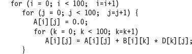
Show the code for MIPS and VMIPS for the DAXPY loop. Assume that the starting addresses of X and Y are in Rx and Ry, respectively.
Answer
DADDIU R4,Rx,#512 ;last address to load
ADD.D F4,F4,F2 ;a × X[i] + Y[i]
DADDIU Rx,Rx,#8 ;increment index to X
DADDIU Ry,Ry,#8 ;increment index to Y
DSUBU R20,R4,Rx ;compute bound
Here is the VMIPS code for DAXPY.
MULVS.D V2,V1,F0 ;vector-scalar multiply
The most dramatic difference is that the vector processor greatly reduces the dynamic instruction bandwidth, executing only 6 instructions versus almost 600 for MIPS. This reduction occurs because the vector operations work on 64 elements and the overhead instructions that constitute nearly half the loop on MIPS are not present in the VMIPS code. When the compiler produces vector instructions for such a sequence and the resulting code spends much of its time running in vector mode, the code is said to be vectorized or vectorizable. Loops can be vectorized when they do not have dependences between iterations of a loop, which are called loop-carried dependences (see Section 4.5).
Another important difference between MIPS and VMIPS is the frequency of pipeline interlocks. In the straightforward MIPS code, every ADD.D must wait for a MUL.D, and every S.D must wait for the ADD.D. On the vector processor, each vector instruction will only stall for the first element in each vector, and then subsequent elements will flow smoothly down the pipeline. Thus, pipeline stalls are required only once per vector instruction, rather than once per vector element. Vector architects call forwarding of element-dependent operations chaining, in that the dependent operations are “chained” together. In this example, the pipeline stall frequency on MIPS will be about 64× higher than it is on VMIPS. Software pipelining or loop unrolling (Appendix H) can reduce the pipeline stalls on MIPS; however, the large difference in instruction bandwidth cannot be reduced substantially.
Vector Execution Time
The execution time of a sequence of vector operations primarily depends on three factors: (1) the length of the operand vectors, (2) structural hazards among the operations, and (3) the data dependences. Given the vector length and the initiation rate, which is the rate at which a vector unit consumes new operands and produces new results, we can compute the time for a single vector instruction. All modern vector computers have vector functional units with multiple parallel pipelines (or lanes) that can produce two or more results per clock cycle, but they may also have some functional units that are not fully pipelined. For simplicity, our VMIPS implementation has one lane with an initiation rate of one element per clock cycle for individual operations. Thus, the execution time in clock cycles for a single vector instruction is approximately the vector length.
To simplify the discussion of vector execution and vector performance, we use the notion of a convoy, which is the set of vector instructions that could potentially execute together. As we shall soon see, you can estimate performance of a section of code by counting the number of convoys. The instructions in a convoy must not contain any structural hazards; if such hazards were present, the instructions would need to be serialized and initiated in different convoys. To keep the analysis simple, we assume that a convoy of instructions must complete execution before any other instructions (scalar or vector) can begin execution.
It might seem that in addition to vector instruction sequences with structural hazards, sequences with read-after-write dependency hazards should also be in separate convoys, but chaining allows them to be in the same convoy.
Chaining allows a vector operation to start as soon as the individual elements of its vector source operand become available: The results from the first functional unit in the chain are “forwarded” to the second functional unit. In practice, we often implement chaining by allowing the processor to read and write a particular vector register at the same time, albeit to different elements. Early implementations of chaining worked just like forwarding in scalar pipelining, but this restricted the timing of the source and destination instructions in the chain. Recent implementations use flexible chaining, which allows a vector instruction to chain to essentially any other active vector instruction, assuming that we don’t generate a structural hazard. All modern vector architectures support flexible chaining, which we assume in this chapter.
To turn convoys into execution time we need a timing metric to estimate the time for a convoy. It is called a chime, which is simply the unit of time taken to execute one convoy. Thus, a vector sequence that consists of m convoys executes in m chimes; for a vector length of n, for VMIPS this is approximately m × n clock cycles. The chime approximation ignores some processor-specific overheads, many of which are dependent on vector length. Hence, measuring time in chimes is a better approximation for long vectors than for short ones. We will use the chime measurement, rather than clock cycles per result, to indicate explicitly that we are ignoring certain overheads.
If we know the number of convoys in a vector sequence, we know the execution time in chimes. One source of overhead ignored in measuring chimes is any limitation on initiating multiple vector instructions in a single clock cycle. If only one vector instruction can be initiated in a clock cycle (the reality in most vector processors), the chime count will underestimate the actual execution time of a convoy. Because the length of vectors is typically much greater than the number of instructions in the convoy, we will simply assume that the convoy executes in one chime.
Example
Show how the following code sequence lays out in convoys, assuming a single copy of each vector functional unit:
MULVS.D V2,V1,F0 ;vector-scalar multiply
ADDVV.D V4,V2,V3 ;add two vectors
How many chimes will this vector sequence take? How many cycles per FLOP (floating-point operation) are needed, ignoring vector instruction issue overhead?
Answer
The first convoy starts with the first LV instruction. The MULVS.D is dependent on the first LV, but chaining allows it to be in the same convoy.
The second LV instruction must be in a separate convoy since there is a structural hazard on the load/store unit for the prior LV instruction. The ADDVV.D is dependent on the second LV, but it can again be in the same convoy via chaining. Finally, the SV has a structural hazard on the LV in the second convoy, so it must go in the third convoy. This analysis leads to the following layout of vector instructions into convoys:
The sequence requires three convoys. Since the sequence takes three chimes and there are two floating-point operations per result, the number of cycles per FLOP is 1.5 (ignoring any vector instruction issue overhead). Note that, although we allow the LV and MULVS.D both to execute in the first convoy, most vector machines will take two clock cycles to initiate the instructions.
This example shows that the chime approximation is reasonably accurate for long vectors. For example, for 64-element vectors, the time in chimes is 3, so the sequence would take about 64 × 3 or 192 clock cycles. The overhead of issuing convoys in two separate clock cycles would be small.
Another source of overhead is far more significant than the issue limitation. The most important source of overhead ignored by the chime model is vector start-up time. The start-up time is principally determined by the pipelining latency of the vector functional unit. For VMIPS, we will use the same pipeline depths as the Cray-1, although latencies in more modern processors have tended to increase, especially for vector loads. All functional units are fully pipelined. The pipeline depths are 6 clock cycles for floating-point add, 7 for floating-point multiply, 20 for floating-point divide, and 12 for vector load.
Given these vector basics, the next several subsections will give optimizations that either improve the performance or increase the types of programs that can run well on vector architectures. In particular, they will answer the questions:
The rest of this section introduces each of these optimizations of the vector architecture, and Appendix G goes into greater depth.
Multiple Lanes: Beyond One Element per Clock Cycle
A critical advantage of a vector instruction set is that it allows software to pass a large amount of parallel work to hardware using only a single short instruction. A single vector instruction can include scores of independent operations yet be encoded in the same number of bits as a conventional scalar instruction. The parallel semantics of a vector instruction allow an implementation to execute these elemental operations using a deeply pipelined functional unit, as in the VMIPS implementation we’ve studied so far; an array of parallel functional units; or a combination of parallel and pipelined functional units. Figure 4.4 illustrates how to improve vector performance by using parallel pipelines to execute a vector add instruction.

Figure 4.4 Using multiple functional units to improve the performance of a single vector add instruction, C = A + B. The vector processor (a) on the left has a single add pipeline and can complete one addition per cycle. The vector processor (b) on the right has four add pipelines and can complete four additions per cycle. The elements within a single vector add instruction are interleaved across the four pipelines. The set of elements that move through the pipelines together is termed an element group. (Reproduced with permission from Asanovic [1998].)
The VMIPS instruction set has the property that all vector arithmetic instructions only allow element N of one vector register to take part in operations with element N from other vector registers. This dramatically simplifies the construction of a highly parallel vector unit, which can be structured as multiple parallel lanes. As with a traffic highway, we can increase the peak throughput of a vector unit by adding more lanes. Figure 4.5 shows the structure of a four-lane vector unit. Thus, going to four lanes from one lane reduces the number of clocks for a chime from 64 to 16. For multiple lanes to be advantageous, both the applications and the architecture must support long vectors; otherwise, they will execute so quickly that you’ll run out of instruction bandwidth, requiring ILP techniques (see Chapter 3) to supply enough vector instructions.

Figure 4.5 Structure of a vector unit containing four lanes. The vector register storage is divided across the lanes, with each lane holding every fourth element of each vector register. The figure shows three vector functional units: an FP add, an FP multiply, and a load-store unit. Each of the vector arithmetic units contains four execution pipelines, one per lane, which act in concert to complete a single vector instruction. Note how each section of the vector register file only needs to provide enough ports for pipelines local to its lane. This figure does not show the path to provide the scalar operand for vector-scalar instructions, but the scalar processor (or control processor) broadcasts a scalar value to all lanes.
Each lane contains one portion of the vector register file and one execution pipeline from each vector functional unit. Each vector functional unit executes vector instructions at the rate of one element group per cycle using multiple pipelines, one per lane. The first lane holds the first element (element 0) for all vector registers, and so the first element in any vector instruction will have its source and destination operands located in the first lane. This allocation allows the arithmetic pipeline local to the lane to complete the operation without communicating with other lanes. Accessing main memory also requires only intralane wiring. Avoiding interlane communication reduces the wiring cost and register file ports required to build a highly parallel execution unit, and helps explain why vector computers can complete up to 64 operations per clock cycle (2 arithmetic units and 2 load/store units across 16 lanes).
Adding multiple lanes is a popular technique to improve vector performance as it requires little increase in control complexity and does not require changes to existing machine code. It also allows designers to trade off die area, clock rate, voltage, and energy without sacrificing peak performance. If the clock rate of a vector processor is halved, doubling the number of lanes will retain the same potential performance.
Vector-Length Registers: Handling Loops Not Equal to 64
A vector register processor has a natural vector length determined by the number of elements in each vector register. This length, which is 64 for VMIPS, is unlikely to match the real vector length in a program. Moreover, in a real program the length of a particular vector operation is often unknown at compile time. In fact, a single piece of code may require different vector lengths. For example, consider this code:
![]()
The size of all the vector operations depends on n, which may not even be known until run time! The value of n might also be a parameter to a procedure containing the above loop and therefore subject to change during execution.
The solution to these problems is to create a vector-length register (VLR). The VLR controls the length of any vector operation, including a vector load or store. The value in the VLR, however, cannot be greater than the length of the vector registers. This solves our problem as long as the real length is less than or equal to the maximum vector length (MVL). The MVL determines the number of data elements in a vector of an architecture. This parameter means the length of vector registers can grow in later computer generations without changing the instruction set; as we shall see in the next section, multimedia SIMD extensions have no equivalent of MVL, so they change the instruction set every time they increase their vector length.
What if the value of n is not known at compile time and thus may be greater than the MVL? To tackle the second problem where the vector is longer than the maximum length, a technique called strip mining is used. Strip mining is the generation of code such that each vector operation is done for a size less than or equal to the MVL. We create one loop that handles any number of iterations that is a multiple of the MVL and another loop that handles any remaining iterations and must be less than the MVL. In practice, compilers usually create a single strip-mined loop that is parameterized to handle both portions by changing the length. We show the strip-mined version of the DAXPY loop in C:

The term n/MVL represents truncating integer division. The effect of this loop is to block the vector into segments that are then processed by the inner loop. The length of the first segment is (n % MVL), and all subsequent segments are of length MVL. Figure 4.6 shows how to split the long vector into segments.

Figure 4.6 A vector of arbitrary length processed with strip mining. All blocks but the first are of length MVL, utilizing the full power of the vector processor. In this figure, we use the variable m for the expression (n % MVL). (The C operator % is modulo.)
The inner loop of the preceding code is vectorizable with length VL, which is equal to either (n % MVL) or MVL. The VLR register must be set twice in the code, once at each place where the variable VL in the code is assigned.
Vector Mask Registers: Handling IF Statements in Vector Loops
From Amdahl’s law, we know that the speedup on programs with low to moderate levels of vectorization will be very limited. The presence of conditionals (IF statements) inside loops and the use of sparse matrices are two main reasons for lower levels of vectorization. Programs that contain IF statements in loops cannot be run in vector mode using the techniques we have discussed so far because the IF statements introduce control dependences into a loop. Likewise, we cannot implement sparse matrices efficiently using any of the capabilities we have seen so far. We discuss strategies for dealing with conditional execution here, leaving the discussion of sparse matrices for later.
Consider the following loop written in C:

This loop cannot normally be vectorized because of the conditional execution of the body; however, if the inner loop could be run for the iterations for which X[i] ≠ 0, then the subtraction could be vectorized.
The common extension for this capability is vector-mask control. Mask registers essentially provide conditional execution of each element operation in a vector instruction. The vector-mask control uses a Boolean vector to control the execution of a vector instruction, just as conditionally executed instructions use a Boolean condition to determine whether to execute a scalar instruction. When the vector-mask register is enabled, any vector instructions executed operate only on the vector elements whose corresponding entries in the vector-mask register are one. The entries in the destination vector register that correspond to a zero in the mask register are unaffected by the vector operation. Clearing the vector-mask register sets it to all ones, making subsequent vector instructions operate on all vector elements. We can now use the following code for the previous loop, assuming that the starting addresses of X and Y are in Rx and Ry, respectively:

Compiler writers call the transformation to change an IF statement to a straight-line code sequence using conditional execution if conversion.
Using a vector-mask register does have overhead, however. With scalar architectures, conditionally executed instructions still require execution time when the condition is not satisfied. Nonetheless, the elimination of a branch and the associated control dependences can make a conditional instruction faster even if it sometimes does useless work. Similarly, vector instructions executed with a vector mask still take the same execution time, even for the elements where the mask is zero. Likewise, even with a significant number of zeros in the mask, using vector-mask control may still be significantly faster than using scalar mode.
As we shall see in Section 4.4, one difference between vector processors and GPUs is the way they handle conditional statements. Vector processors make the mask registers part of the architectural state and rely on compilers to manipulate mask registers explicitly. In contrast, GPUs get the same effect using hardware to manipulate internal mask registers that are invisible to GPU software. In both cases, the hardware spends the time to execute a vector element whether the mask is zero or one, so the GFLOPS rate drops when masks are used.
Memory Banks: Supplying Bandwidth for Vector Load/Store Units
The behavior of the load/store vector unit is significantly more complicated than that of the arithmetic functional units. The start-up time for a load is the time to get the first word from memory into a register. If the rest of the vector can be supplied without stalling, then the vector initiation rate is equal to the rate at which new words are fetched or stored. Unlike simpler functional units, the initiation rate may not necessarily be one clock cycle because memory bank stalls can reduce effective throughput.
Typically, penalties for start-ups on load/store units are higher than those for arithmetic units—over 100 clock cycles on many processors. For VMIPS we assume a start-up time of 12 clock cycles, the same as the Cray-1. (More recent vector computers use caches to bring down latency of vector loads and stores.)
To maintain an initiation rate of one word fetched or stored per clock, the memory system must be capable of producing or accepting this much data. Spreading accesses across multiple independent memory banks usually delivers the desired rate. As we will soon see, having significant numbers of banks is useful for dealing with vector loads or stores that access rows or columns of data.
Most vector processors use memory banks, which allow multiple independent accesses rather than simple memory interleaving for three reasons:
In combination, these features lead to a large number of independent memory banks, as the following example shows.
Example
The largest configuration of a Cray T90 (Cray T932) has 32 processors, each capable of generating 4 loads and 2 stores per clock cycle. The processor clock cycle is 2.167 ns, while the cycle time of the SRAMs used in the memory system is 15 ns. Calculate the minimum number of memory banks required to allow all processors to run at full memory bandwidth.
Answer
The maximum number of memory references each cycle is 192: 32 processors times 6 references per processor. Each SRAM bank is busy for 15/2.167 = 6.92 clock cycles, which we round up to 7 processor clock cycles. Therefore, we require a minimum of 192 × 7 = 1344 memory banks!
The Cray T932 actually has 1024 memory banks, so the early models could not sustain full bandwidth to all processors simultaneously. A subsequent memory upgrade replaced the 15 ns asynchronous SRAMs with pipelined synchronous SRAMs that more than halved the memory cycle time, thereby providing sufficient bandwidth.
Taking a higher level perspective, vector load/store units play a similar role to prefetch units in scalar processors in that both try to deliver data bandwidth by supplying processors with streams of data.
Stride: Handling Multidimensional Arrays in Vector Architectures
The position in memory of adjacent elements in a vector may not be sequential. Consider this straightforward code for matrix multiply in C:
We could vectorize the multiplication of each row of B with each column of D and strip-mine the inner loop with k as the index variable.
To do so, we must consider how to address adjacent elements in B and adjacent elements in D. When an array is allocated memory, it is linearized and must be laid out in either row-major (as in C) or column-major (as in Fortran) order. This linearization means that either the elements in the row or the elements in the column are not adjacent in memory. For example, the C code above allocates in row-major order, so the elements of D that are accessed by iterations in the inner loop are separated by the row size times 8 (the number of bytes per entry) for a total of 800 bytes. In Chapter 2, we saw that blocking could improve locality in cache-based systems. For vector processors without caches, we need another technique to fetch elements of a vector that are not adjacent in memory.
This distance separating elements to be gathered into a single register is called the stride. In this example, matrix D has a stride of 100 double words (800 bytes), and matrix B would have a stride of 1 double word (8 bytes). For column-major order, which is used by Fortran, the strides would be reversed. Matrix D would have a stride of 1, or 1 double word (8 bytes), separating successive elements, while matrix B would have a stride of 100, or 100 double words (800 bytes). Thus, without reordering the loops, the compiler can’t hide the long distances between successive elements for both B and D.
Once a vector is loaded into a vector register, it acts as if it had logically adjacent elements. Thus, a vector processor can handle strides greater than one, called non-unit strides, using only vector load and vector store operations with stride capability. This ability to access nonsequential memory locations and to reshape them into a dense structure is one of the major advantages of a vector processor. Caches inherently deal with unit stride data; increasing block size can help reduce miss rates for large scientific datasets with unit stride, but increasing block size can even have a negative effect for data that are accessed with non-unit strides. While blocking techniques can solve some of these problems (see Chapter 2), the ability to access data efficiently that is not contiguous remains an advantage for vector processors on certain problems, as we shall see in Section 4.7.
On VMIPS, where the addressable unit is a byte, the stride for our example would be 800. The value must be computed dynamically, since the size of the matrix may not be known at compile time or—just like vector length—may change for different executions of the same statement. The vector stride, like the vector starting address, can be put in a general-purpose register. Then the VMIPS instruction LVWS ( load vector with stride) fetches the vector into a vector register. Likewise, when storing a non-unit stride vector, use the instruction SVWS (store vector with stride).
Supporting strides greater than one complicates the memory system. Once we introduce non-unit strides, it becomes possible to request accesses from the same bank frequently. When multiple accesses contend for a bank, a memory bank conflict occurs, thereby stalling one access. A bank conflict and, hence, a stall will occur if
Example
Suppose we have 8 memory banks with a bank busy time of 6 clocks and a total memory latency of 12 cycles. How long will it take to complete a 64-element vector load with a stride of 1? With a stride of 32?
Answer
Since the number of banks is larger than the bank busy time, for a stride of 1 the load will take 12 + 64 = 76 clock cycles, or 1.2 clock cycles per element. The worst possible stride is a value that is a multiple of the number of memory banks, as in this case with a stride of 32 and 8 memory banks. Every access to memory (after the first one) will collide with the previous access and will have to wait for the 6-clock-cycle bank busy time. The total time will be 12 + 1 + 6 * 63 = 391 clock cycles, or 6.1 clock cycles per element.
Gather-Scatter: Handling Sparse Matrices in Vector Architectures
As mentioned above, sparse matrices are commonplace so it is important to have techniques to allow programs with sparse matrices to execute in vector mode. In a sparse matrix, the elements of a vector are usually stored in some compacted form and then accessed indirectly. Assuming a simplified sparse structure, we might see code that looks like this:
![]()
This code implements a sparse vector sum on the arrays A and C, using index vectors K and M to designate the nonzero elements of A and C. (A and C must have the same number of nonzero elements— n of them—so K and M are the same size.)
The primary mechanism for supporting sparse matrices is gather-scatter operations using index vectors. The goal of such operations is to support moving between a compressed representation (i.e., zeros are not included) and normal representation (i.e., the zeros are included) of a sparse matrix. A gather operation takes an index vector and fetches the vector whose elements are at the addresses given by adding a base address to the offsets given in the index vector. The result is a dense vector in a vector register. After these elements are operated on in dense form, the sparse vector can be stored in expanded form by a scatter store, using the same index vector. Hardware support for such operations is called gather-scatter and it appears on nearly all modern vector processors. The VMIPS instructions are LVI (load vector indexed or gather) and SVI (store vector indexed or scatter). For example, if Ra, Rc, Rk, and Rm contain the starting addresses of the vectors in the previous sequence, we can code the inner loop with vector instructions such as:
This technique allows code with sparse matrices to run in vector mode. A simple vectorizing compiler could not automatically vectorize the source code above because the compiler would not know that the elements of K are distinct values, and thus that no dependences exist. Instead, a programmer directive would tell the compiler that it was safe to run the loop in vector mode.
Although indexed loads and stores (gather and scatter) can be pipelined, they typically run much more slowly than non-indexed loads or stores, since the memory banks are not known at the start of the instruction. Each element has an individual address, so they can’t be handled in groups, and there can be conflicts at many places throughout the memory system. Thus, each individual access incurs significant latency. However, as Section 4.7 shows, a memory system can deliver better performance by designing for this case and by using more hardware resources versus when architects have a laissez faire attitude toward such accesses.
As we shall see in Section 4.4, all loads are gathers and all stores are scatters in GPUs. To avoid running slowly in the frequent case of unit strides, it is up to the GPU programmer to ensure that all the addresses in a gather or scatter are to adjacent locations. In addition, the GPU hardware must recognize the sequence of these addresses during execution to turn the gathers and scatters into the more efficient unit stride accesses to memory.
Programming Vector Architectures
An advantage of vector architectures is that compilers can tell programmers at compile time whether a section of code will vectorize or not, often giving hints as to why it did not vectorize the code. This straightforward execution model allows experts in other domains to learn how to improve performance by revising their code or by giving hints to the compiler when it’s OK to assume independence between operations, such as for gather-scatter data transfers. It is this dialog between the compiler and the programmer, with each side giving hints to the other on how to improve performance, that simplifies programming of vector computers.
Today, the main factor that affects the success with which a program runs in vector mode is the structure of the program itself: Do the loops have true data dependences (see Section 4.5), or can they be restructured so as not to have such dependences? This factor is influenced by the algorithms chosen and, to some extent, by how they are coded.
As an indication of the level of vectorization achievable in scientific programs, let’s look at the vectorization levels observed for the Perfect Club benchmarks. Figure 4.7 shows the percentage of operations executed in vector mode for two versions of the code running on the Cray Y-MP. The first version is that obtained with just compiler optimization on the original code, while the second version uses extensive hints from a team of Cray Research programmers. Several studies of the performance of applications on vector processors show a wide variation in the level of compiler vectorization.

Figure 4.7 Level of vectorization among the Perfect Club benchmarks when executed on the Cray Y-MP [Vajapeyam 1991]. The first column shows the vectorization level obtained with the compiler without hints, while the second column shows the results after the codes have been improved with hints from a team of Cray Research programmers.
The hint-rich versions show significant gains in vectorization level for codes the compiler could not vectorize well by itself, with all codes now above 50% vectorization. The median vectorization improved from about 70% to about 90%.
4.3 SIMD Instruction Set Extensions for Multimedia
SIMD Multimedia Extensions started with the simple observation that many media applications operate on narrower data types than the 32-bit processors were optimized for. Many graphics systems used 8 bits to represent each of the three primary colors plus 8 bits for transparency. Depending on the application, audio samples are usually represented with 8 or 16 bits. By partitioning the carry chains within, say, a 256-bit adder, a processor could perform simultaneous operations on short vectors of thirty-two 8-bit operands, sixteen 16-bit operands, eight 32-bit operands, or four 64-bit operands. The additional cost of such partitioned adders was small. Figure 4.8 summarizes typical multimedia SIMD instructions. Like vector instructions, a SIMD instruction specifies the same operation on vectors of data. Unlike vector machines with large register files such as the VMIPS vector register, which can hold as many as sixty-four 64-bit elements in each of 8 vector registers, SIMD instructions tend to specify fewer operands and hence use much smaller register files.

Figure 4.8 Summary of typical SIMD multimedia support for 256-bit-wide operations. Note that the IEEE 754-2008 floating-point standard added half-precision (16-bit) and quad-precision (128-bit) floating-point operations.
In contrast to vector architectures, which offer an elegant instruction set that is intended to be the target of a vectorizing compiler, SIMD extensions have three major omissions:
These omissions make it harder for the compiler to generate SIMD code and increase the difficulty of programming in SIMD assembly language.
For the x86 architecture, the MMX instructions added in 1996 repurposed the 64-bit floating-point registers, so the basic instructions could perform eight 8-bit operations or four 16-bit operations simultaneously. These were joined by parallel MAX and MIN operations, a wide variety of masking and conditional instructions, operations typically found in digital signal processors, and ad hoc instructions that were believed to be useful in important media libraries. Note that MMX reused the floating-point data transfer instructions to access memory.
The Streaming SIMD Extensions (SSE) successor in 1999 added separate registers that were 128 bits wide, so now instructions could simultaneously perform sixteen 8-bit operations, eight 16-bit operations, or four 32-bit operations. It also performed parallel single-precision floating-point arithmetic. Since SSE had separate registers, it needed separate data transfer instructions. Intel soon added double-precision SIMD floating-point data types via SSE2 in 2001, SSE3 in 2004, and SSE4 in 2007. Instructions with four single-precision floating-point operations or two parallel double-precision operations increased the peak floating-point performance of the x86 computers, as long as programmers place the operands side by side. With each generation, they also added ad hoc instructions whose aim is to accelerate specific multimedia functions perceived to be important.
The Advanced Vector Extensions (AVX), added in 2010, doubles the width of the registers again to 256 bits and thereby offers instructions that double the number of operations on all narrower data types. Figure 4.9 shows AVX instructions useful for double-precision floating-point computations. AVX includes preparations to extend the width to 512 bits and 1024 bits in future generations of the architecture.

Figure 4.9 AVX instructions for x86 architecture useful in double-precision floating-point programs. Packed-double for 256-bit AVX means four 64-bit operands executed in SIMD mode. As the width increases with AVX, it is increasingly important to add data permutation instructions that allow combinations of narrow operands from different parts of the wide registers. AVX includes instructions that shuffle 32-bit, 64-bit, or 128-bit operands within a 256-bit register. For example, BROADCAST replicates a 64-bit operand 4 times in an AVX register. AVX also includes a large variety of fused multiply-add/subtract instructions; we show just two here.
In general, the goal of these extensions has been to accelerate carefully written libraries rather than for the compiler to generate them (see Appendix H), but recent x86 compilers are trying to generate such code, particularly for floating-point-intensive applications.
Given these weaknesses, why are Multimedia SIMD Extensions so popular? First, they cost little to add to the standard arithmetic unit and they were easy to implement. Second, they require little extra state compared to vector architectures, which is always a concern for context switch times. Third, you need a lot of memory bandwidth to support a vector architecture, which many computers don’t have. Fourth, SIMD does not have to deal with problems in virtual memory when a single instruction that can generate 64 memory accesses can get a page fault in the middle of the vector. SIMD extensions use separate data transfers per SIMD group of operands that are aligned in memory, and so they cannot cross page boundaries. Another advantage of short, fixed-length “vectors” of SIMD is that it is easy to introduce instructions that can help with new media standards, such as instructions that perform permutations or instructions that consume either fewer or more operands than vectors can produce. Finally, there was concern about how well vector architectures can work with caches. More recent vector architectures have addressed all of these problems, but the legacy of past flaws shaped the skeptical attitude toward vectors among architects.
Example
To give an idea of what multimedia instructions look like, assume we added 256-bit SIMD multimedia instructions to MIPS. We concentrate on floating-point in this example. We add the suffix “4D” on instructions that operate on four double-precision operands at once. Like vector architectures, you can think of a SIMD processor as having lanes, four in this case. MIPS SIMD will reuse the floating-point registers as operands for 4D instructions, just as double-precision reused single-precision registers in the original MIPS. This example shows MIPS SIMD code for the DAXPY loop. Assume that the starting addresses of X and Y are in Rx and Ry, respectively. Underline the changes to the MIPS code for SIMD.
Answer

The changes were replacing every MIPS double-precision instruction with its 4D equivalent, increasing the increment from 8 to 32, and changing the registers from F2 and F4 to F4 and F8 to get enough space in the register file for four sequential double-precision operands. So that each SIMD lane would have its own copy of the scalar a, we copied the value of F0 into registers F1, F2, and F3. (Real SIMD instruction extensions have an instruction to broadcast a value to all other registers in a group.) Thus, the multiply does F4*F0, F5*F1, F6*F2, and F7*F3. While not as dramatic as the 100× reduction of dynamic instruction bandwidth of VMIPS, SIMD MIPS does get a 4× reduction: 149 versus 578 instructions executed for MIPS.
Programming Multimedia SIMD Architectures
Given the ad hoc nature of the SIMD multimedia extensions, the easiest way to use these instructions has been through libraries or by writing in assembly language.
Recent extensions have become more regular, giving the compiler a more reasonable target. By borrowing techniques from vectorizing compilers, compilers are starting to produce SIMD instructions automatically. For example, advanced compilers today can generate SIMD floating-point instructions to deliver much higher performance for scientific codes. However, programmers must be sure to align all the data in memory to the width of the SIMD unit on which the code is run to prevent the compiler from generating scalar instructions for otherwise vectorizable code.
The Roofline Visual Performance Model
One visual, intuitive way to compare potential floating-point performance of variations of SIMD architectures is the Roofline model [Williams et al. 2009]. It ties together floating-point performance, memory performance, and arithmetic intensity in a two-dimensional graph. Arithmetic intensity is the ratio of floating-point operations per byte of memory accessed. It can be calculated by taking the total number of floating-point operations for a program divided by the total number of data bytes transferred to main memory during program execution. Figure 4.10 shows the relative arithmetic intensity of several example kernels.

Figure 4.10 Arithmetic intensity, specified as the number of floating-point operations to run the program divided by the number of bytes accessed in main memory [Williams et al. 2009]. Some kernels have an arithmetic intensity that scales with problem size, such as dense matrix, but there are many kernels with arithmetic intensities independent of problem size.
Peak floating-point performance can be found using the hardware specifications. Many of the kernels in this case study do not fit in on-chip caches, so peak memory performance is defined by the memory system behind the caches. Note that we need the peak memory bandwidth that is available to the processors, not just at the DRAM pins as in Figure 4.27 on page 325. One way to find the (delivered) peak memory performance is to run the Stream benchmark.
Figure 4.11 shows the Roofline model for the NEC SX-9 vector processor on the left and the Intel Core i7 920 multicore computer on the right. The vertical Y-axis is achievable floating-point performance from 2 to 256 GFLOP/sec. The horizontal X-axis is arithmetic intensity, varying from 1/8th FLOP/DRAM byte accessed to 16 FLOP/ DRAM byte accessed in both graphs. Note that the graph is a log–log scale, and that Rooflines are done just once for a computer.

Figure 4.11 Roofline model for one NEC SX-9 vector processor on the left and the Intel Core i7 920 multicore computer with SIMD Extensions on the right [Williams et al. 2009]. This Roofline is for unit-stride memory accesses and double-precision floating-point performance. NEC SX-9 is a vector supercomputer announced in 2008 that costs millions of dollars. It has a peak DP FP performance of 102.4 GFLOP/sec and a peak memory bandwidth of 162 GBytes/sec from the Stream benchmark. The Core i7 920 has a peak DP FP performance of 42.66 GFLOP/sec and a peak memory bandwidth of 16.4 GBytes/sec. The dashed vertical lines at an arithmetic intensity of 4 FLOP/byte show that both processors operate at peak performance. In this case, the SX-9 at 102.4 FLOP/sec is 2.4× faster than the Core i7 at 42.66 GFLOP/sec. At an arithmetic intensity of 0.25 FLOP/byte, the SX-9 is 10× faster at 40.5 GFLOP/sec versus 4.1 GFLOP/sec for the Core i7.
For a given kernel, we can find a point on the X-axis based on its arithmetic intensity. If we drew a vertical line through that point, the performance of the kernel on that computer must lie somewhere along that line. We can plot a horizontal line showing peak floating-point performance of the computer. Obviously, the actual floating-point performance can be no higher than the horizontal line, since that is a hardware limit.
How could we plot the peak memory performance? Since the X-axis is FLOP/byte and the Y-axis is FLOP/sec, bytes/sec is just a diagonal line at a 45-degree angle in this figure. Hence, we can plot a third line that gives the maximum floating-point performance that the memory system of that computer can support for a given arithmetic intensity. We can express the limits as a formula to plot these lines in the graphs in Figure 4.11:
The horizontal and diagonal lines give this simple model its name and indicate its value. The “Roofline” sets an upper bound on performance of a kernel depending on its arithmetic intensity. If we think of arithmetic intensity as a pole that hits the roof, either it hits the flat part of the roof, which means performance is computationally limited, or it hits the slanted part of the roof, which means performance is ultimately limited by memory bandwidth. In Figure 4.11, the vertical dashed line on the right (arithmetic intensity of 4) is an example of the former and the vertical dashed line on the left (arithmetic intensity of 1/4) is an example of the latter. Given a Roofline model of a computer, you can apply it repeatedly, since it doesn’t vary by kernel.
Note that the “ridge point,” where the diagonal and horizontal roofs meet, offers an interesting insight into the computer. If it is far to the right, then only kernels with very high arithmetic intensity can achieve the maximum performance of that computer. If it is far to the left, then almost any kernel can potentially hit the maximum performance. As we shall see, this vector processor has both much higher memory bandwidth and a ridge point far to the left when compared to other SIMD processors.
Figure 4.11 shows that the peak computational performance of the SX-9 is 2.4× faster than Core i7, but the memory performance is 10× faster. For programs with an arithmetic intensity of 0.25, the SX-9 is 10× faster (40.5 versus 4.1 GFLOP/sec). The higher memory bandwidth moves the ridge point from 2.6 in the Core i7 to 0.6 on the SX-9, which means many more programs can reach peak computational performance on the vector processor.
4.4 Graphics Processing Units
For a few hundred dollars, anyone can buy a GPU with hundreds of parallel floating-point units, which makes high-performance computing more accessible. The interest in GPU computing blossomed when this potential was combined with a programming language that made GPUs easier to program. Hence, many programmers of scientific and multimedia applications today are pondering whether to use GPUs or CPUs.
GPUs and CPUs do not go back in computer architecture genealogy to a common ancestor; there is no Missing Link that explains both. As Section 4.10 describes, the primary ancestors of GPUs are graphics accelerators, as doing graphics well is the reason why GPUs exist. While GPUs are moving toward mainstream computing, they can’t abandon their responsibility to continue to excel at graphics. Thus, the design of GPUs may make more sense when architects ask, given the hardware invested to do graphics well, how can we supplement it to improve the performance of a wider range of applications?
Note that this section concentrates on using GPUs for computing. To see how GPU computing combines with the traditional role of graphics acceleration, see “Graphics and Computing GPUs,” by John Nickolls and David Kirk (Appendix A in the 4th edition of Computer Organization and Design by the same authors as this book).
Since the terminology and some hardware features are quite different from vector and SIMD architectures, we believe it will be easier if we start with the simplified programming model for GPUs before we describe the architecture.
Programming the GPU
CUDA is an elegant solution to the problem of representing parallelism in algorithms, not all algorithms, but enough to matter. It seems to resonate in some way with the way we think and code, allowing an easier, more natural expression of parallelism beyond the task level.
The challenge for the GPU programmer is not simply getting good performance on the GPU, but also in coordinating the scheduling of computation on the system processor and the GPU and the transfer of data between system memory and GPU memory. Moreover, as we see shall see later in this section, GPUs have virtually every type of parallelism that can be captured by the programming environment: multithreading, MIMD, SIMD, and even instruction-level.
NVIDIA decided to develop a C-like language and programming environment that would improve the productivity of GPU programmers by attacking both the challenges of heterogeneous computing and of multifaceted parallelism. The name of their system is CUDA, for Compute Unified Device Architecture. CUDA produces C/C++ for the system processor (host) and a C and C++ dialect for the GPU (device, hence the D in CUDA). A similar programming language is OpenCL, which several companies are developing to offer a vendor-independent language for multiple platforms.
NVIDIA decided that the unifying theme of all these forms of parallelism is the CUDA Thread. Using this lowest level of parallelism as the programming primitive, the compiler and the hardware can gang thousands of CUDA Threads together to utilize the various styles of parallelism within a GPU: multithreading, MIMD, SIMD, and instruction-level parallelism. Hence, NVIDIA classifies the CUDA programming model as Single Instruction, Multiple Thread (SIMT). For reasons we shall soon see, these threads are blocked together and executed in groups of 32 threads, called a Thread Block. We call the hardware that executes a whole block of threads a multithreaded SIMD Processor.
We need just a few details before we can give an example of a CUDA program:
name<<<dimGrid, dimBlock>>>(… parameter list …)
where dimGrid and dimBlock specify the dimensions of the code (in blocks) and the dimensions of a block (in threads).
Before seeing the CUDA code, let’s start with conventional C code for the DAXPY loop from Section 4.2:

Below is the CUDA version. We launch n threads, one per vector element, with 256 CUDA Threads per thread block in a multithreaded SIMD Processor. The GPU function starts by calculating the corresponding element index i based on the block ID, the number of threads per block, and the thread ID. As long as this index is within the array (i < n), it performs the multiply and add.

Comparing the C and CUDA codes, we see a common pattern to parallelizing data-parallel CUDA code. The C version has a loop where each iteration is independent of the others, allowing the loop to be transformed straightforwardly into a parallel code where each loop iteration becomes an independent thread. (As mentioned above and described in detail in Section 4.5, vectorizing compilers also rely on a lack of dependences between iterations of a loop, which are called loop carried dependences.) The programmer determines the parallelism in CUDA explicitly by specifying the grid dimensions and the number of threads per SIMD Processor. By assigning a single thread to each element, there is no need to synchronize among threads when writing results to memory.
The GPU hardware handles parallel execution and thread management; it is not done by applications or by the operating system. To simplify scheduling by the hardware, CUDA requires that thread blocks be able to execute independently and in any order. Different thread blocks cannot communicate directly, although they can coordinate using atomic memory operations in Global Memory.
As we shall soon see, many GPU hardware concepts are not obvious in CUDA. That is a good thing from a programmer productivity perspective, but most programmers are using GPUs instead of CPUs to get performance. Performance programmers must keep the GPU hardware in mind when writing in CUDA. For reasons explained shortly, they know that they need to keep groups of 32 threads together in control flow to get the best performance from multithreaded SIMD Processors, and create many more threads per multithreaded SIMD Processor to hide latency to DRAM. They also need to keep the data addresses localized in one or a few blocks of memory to get the expected memory performance.
Like many parallel systems, a compromise between productivity and performance is for CUDA to include intrinsics to give programmers explicit control of the hardware. The struggle between productivity on one hand versus allowing the programmer to be able to express anything that the hardware can do on the other happens often in parallel computing. It will be interesting to see how the language evolves in this classic productivity–performance battle as well as to see if CUDA becomes popular for other GPUs or even other architectural styles.
NVIDIA GPU Computational Structures
The uncommon heritage mentioned above helps explain why GPUs have their own architectural style and their own terminology independent from CPUs. One obstacle to understanding GPUs has been the jargon, with some terms even having misleading names. This obstacle has been surprisingly difficult to overcome, as the many rewrites of this chapter can attest. To try to bridge the twin goals of making the architecture of GPUs understandable and learning the many GPU terms with non traditional definitions, our final solution is to use the CUDA terminology for software but initially use more descriptive terms for the hardware, sometimes borrowing terms used by OpenCL. Once we explain the GPU architecture in our terms, we’ll map them into the official jargon of NVIDIA GPUs.
From left to right, Figure 4.12 lists the more descriptive term used in this section, the closest term from mainstream computing, the official NVIDIA GPU term in case you are interested, and then a short description of the term. The rest of this section explains the microarchitetural features of GPUs using these descriptive terms from the left of the figure.

Figure 4.12 Quick guide to GPU terms used in this chapter. We use the first column for hardware terms. Four groups cluster these 11 terms. From top to bottom: Program Abstractions, Machine Objects, Processing Hardware, and Memory Hardware. Figure 4.21 on page 309 associates vector terms with the closest terms here, and Figure 4.24 on page 313 and Figure 4.25 on page 314 reveal the official CUDA/NVIDIA and AMD terms and definitions along with the terms used by OpenCL.
We use NVIDIA systems as our example as they are representative of GPU architectures. Specifically, we follow the terminology of the CUDA parallel programming language above and use the Fermi architecture as the example (see Section 4.7).
Like vector architectures, GPUs work well only with data-level parallel problems. Both styles have gather-scatter data transfers and mask registers, and GPU processors have even more registers than do vector processors. Since they do not have a close-by scalar processor, GPUs sometimes implement a feature at runtime in hardware that vector computers implement at compiler time in software. Unlike most vector architectures, GPUs also rely on multithreading within a single multi-threaded SIMD processor to hide memory latency (see Chapters 2 and 3). However, efficient code for both vector architectures and GPUs requires programmers to think in groups of SIMD operations.
A Grid is the code that runs on a GPU that consists of a set of Thread Blocks. Figure 4.12 draws the analogy between a grid and a vectorized loop and between a Thread Block and the body of that loop (after it has been strip-mined, so that it is a full computation loop). To give a concrete example, let’s suppose we want to multiply two vectors together, each 8192 elements long. We’ll return to this example throughout this section. Figure 4.13 shows the relationship between this example and these first two GPU terms. The GPU code that works on the whole 8192 element multiply is called a Grid (or vectorized loop). To break it down into more manageable sizes, a Grid is composed of Thread Blocks (or body of a vectorized loop), each with up to 512 elements. Note that a SIMD instruction executes 32 elements at a time. With 8192 elements in the vectors, this example thus has 16 Thread Blocks since 16 = 8192 ÷ 512. The Grid and Thread Block are programming abstractions implemented in GPU hardware that help programmers organize their CUDA code. (The Thread Block is analogous to a strip-minded vector loop with a vector length of 32.)

Figure 4.13 The mapping of a Grid (vectorizable loop), Thread Blocks (SIMD basic blocks), and threads of SIMD instructions to a vector–vector multiply, with each vector being 8192 elements long. Each thread of SIMD instructions calculates 32 elements per instruction, and in this example each Thread Block contains 16 threads of SIMD instructions and the Grid contains 16 Thread Blocks. The hardware Thread Block Scheduler assigns Thread Blocks to multithreaded SIMD Processors and the hardware Thread Scheduler picks which thread of SIMD instructions to run each clock cycle within a SIMD Processor. Only SIMD Threads in the same Thread Block can communicate via Local Memory. (The maximum number of SIMD Threads that can execute simultaneously per Thread Block is 16 for Tesla-generation GPUs and 32 for the later Fermi-generation GPUs.)
A Thread Block is assigned to a processor that executes that code, which we call a multithreaded SIMD Processor, by the Thread Block Scheduler. The Thread Block Scheduler has some similarities to a control processor in a vector architecture. It determines the number of thread blocks needed for the loop and keeps allocating them to different multithreaded SIMD Processors until the loop is completed. In this example, it would send 16 Thread Blocks to multithreaded SIMD Processors to compute all 8192 elements of this loop.
Figure 4.14 shows a simplified block diagram of a multithreaded SIMD Processor. It is similar to a Vector Processor, but it has many parallel functional units instead of a few that are deeply pipelined, as does a Vector Processor. In the programming example in Figure 4.13, each multithreaded SIMD Processor is assigned 512 elements of the vectors to work on. SIMD Processors are full processors with separate PCs and are programmed using threads (see Chapter 3).
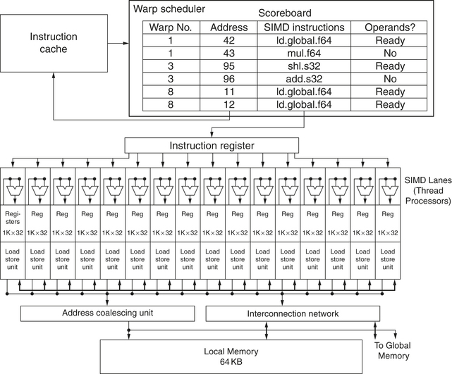
Figure 4.14 Simplified block diagram of a Multithreaded SIMD Processor. It has 16 SIMD lanes. The SIMD Thread Scheduler has, say, 48 independent threads of SIMD instructions that it schedules with a table of 48 PCs.
The GPU hardware then contains a collection of multithreaded SIMD Processors that execute a Grid of Thread Blocks (bodies of vectorized loop); that is, a GPU is a multiprocessor composed of multithreaded SIMD Processors.
The first four implementations of the Fermi architecture have 7, 11, 14, or 15 multithreaded SIMD Processors; future versions may have just 2 or 4. To provide transparent scalability across models of GPUs with differing number of multithreaded SIMD Processors, the Thread Block Scheduler assigns Thread Blocks (bodies of a vectorized loop) to multithreaded SIMD Processors. Figure 4.15 shows the floor plan of the GTX 480 implementation of the Fermi architecture.

Figure 4.15 Floor plan of the Fermi GTX 480 GPU. This diagram shows 16 multithreaded SIMD Processors. The Thread Block Scheduler is highlighted on the left. The GTX 480 has 6 GDDR5 ports, each 64 bits wide, supporting up to 6 GB of capacity. The Host Interface is PCI Express 2.0 × 16. Giga Thread is the name of the scheduler that distributes thread blocks to Multiprocessors, each of which has its own SIMD Thread Scheduler.
Dropping down one more level of detail, the machine object that the hardware creates, manages, schedules, and executes is a thread of SIMD instructions. It is a traditional thread that contains exclusively SIMD instructions. These threads of SIMD instructions have their own PCs and they run on a multithreaded SIMD Processor. The SIMD Thread Scheduler includes a scoreboard that lets it know which threads of SIMD instructions are ready to run, and then it sends them off to a dispatch unit to be run on the multithreaded SIMD Processor. It is identical to a hardware thread scheduler in a traditional multithreaded processor (see Chapter 3), just that it is scheduling threads of SIMD instructions. Thus, GPU hardware has two levels of hardware schedulers: (1) the Thread Block Scheduler that assigns Thread Blocks (bodies of vectorized loops) to multithreaded SIMD Processors, which ensures that thread blocks are assigned to the processors whose local memories have the corresponding data, and (2) the SIMD Thread Scheduler within a SIMD Processor, which schedules when threads of SIMD instructions should run.
The SIMD instructions of these threads are 32 wide, so each thread of SIMD instructions in this example would compute 32 of the elements of the computation. In this example, Thread Blocks would contain 512/32 = 16 SIMD threads (see Figure 4.13).
Since the thread consists of SIMD instructions, the SIMD Processor must have parallel functional units to perform the operation. We call them SIMD Lanes, and they are quite similar to the Vector Lanes in Section 4.2.
The number of lanes per SIMD processor varies across GPU generations. With Fermi, each 32-wide thread of SIMD instructions is mapped to 16 physical SIMD Lanes, so each SIMD instruction in a thread of SIMD instructions takes two clock cycles to complete. Each thread of SIMD instructions is executed in lock step and only scheduled at the beginning. Staying with the analogy of a SIMD Processor as a vector processor, you could say that it has 16 lanes, the vector length would be 32, and the chime is 2 clock cycles. (This wide but shallow nature is why we use the term SIMD Processor instead of vector processor as it is more descriptive.)
Since by definition the threads of SIMD instructions are independent, the SIMD Thread Scheduler can pick whatever thread of SIMD instructions is ready, and need not stick with the next SIMD instruction in the sequence within a thread. The SIMD Thread Scheduler includes a scoreboard (see Chapter 3) to keep track of up to 48 threads of SIMD instructions to see which SIMD instruction is ready to go. This scoreboard is needed because memory access instructions can take an unpredictable number of clock cycles due to memory bank conflicts, for example. Figure 4.16 shows the SIMD Thread Scheduler picking threads of SIMD instructions in a different order over time. The assumption of GPU architects is that GPU applications have so many threads of SIMD instructions that multithreading can both hide the latency to DRAM and increase utilization of multithreaded SIMD Processors. However, to hedge their bets, the recent NVIDIA Fermi GPU includes an L2 cache (see Section 4.7).

Figure 4.16 Scheduling of threads of SIMD instructions. The scheduler selects a ready thread of SIMD instructions and issues an instruction synchronously to all the SIMD Lanes executing the SIMD thread. Because threads of SIMD instructions are independent, the scheduler may select a different SIMD thread each time.
Continuing our vector multiply example, each multithreaded SIMD Processor must load 32 elements of two vectors from memory into registers, perform the multiply by reading and writing registers, and store the product back from registers into memory. To hold these memory elements, a SIMD Processor has an impressive 32,768 32-bit registers. Just like a vector processor, these registers are divided logically across the vector lanes or, in this case, SIMD Lanes. Each SIMD Thread is limited to no more than 64 registers, so you might think of a SIMD Thread as having up to 64 vector registers, with each vector register having 32 elements and each element being 32 bits wide. (Since double-precision floating-point operands use two adjacent 32-bit registers, an alternative view is that each SIMD Thread has 32 vector registers of 32 elements, each of which is 64 bits wide.)
Since Fermi has 16 physical SIMD Lanes, each contains 2048 registers. (Rather than trying to design hardware registers with many read ports and write ports per bit, GPUs will use simpler memory structures but divide them into banks to get sufficient bandwidth, just as vector processors do.) Each CUDA Thread gets one element of each of the vector registers. To handle the 32 elements of each thread of SIMD instructions with 16 SIMD Lanes, the CUDA Threads of a Thread block collectively can use up to half of the 2048 registers.
To be able to execute many threads of SIMD instructions, each is dynamically allocated a set of the physical registers on each SIMD Processor when threads of SIMD instructions are created and freed when the SIMD Thread exits.
Note that a CUDA thread is just a vertical cut of a thread of SIMD instructions, corresponding to one element executed by one SIMD Lane. Beware that CUDA Threads are very different from POSIX threads; you can’t make arbitrary system calls from a CUDA Thread.
NVIDA GPU Instruction Set Architecture
Unlike most system processors, the instruction set target of the NVIDIA compilers is an abstraction of the hardware instruction set. PTX (Parallel Thread Execution) provides a stable instruction set for compilers as well as compatibility across generations of GPUs. The hardware instruction set is hidden from the programmer. PTX instructions describe the operations on a single CUDA thread, and usually map one-to-one with hardware instructions, but one PTX can expand to many machine instructions, and vice versa. PTX uses virtual registers, so the compiler figures out how many physical vector registers a SIMD thread needs, and then an optimizer divides the available register storage between the SIMD threads. This optimizer also eliminates dead code, folds instructions together, and calculates places where branches might diverge and places where diverged paths could converge.
While there is some similarity between the x86 microarchitectures and PTX, in that both translate to an internal form (microinstructions for x86), the difference is that this translation happens in hardware at runtime during execution on the x86 versus in software and load time on a GPU.
The format of a PTX instruction is
where d is the destination operand; a, b, and c are source operands; and the operation type is one of the following:
| Type | .type Specifier |
|---|---|
| Untyped bits 8, 16, 32, and 64 bits | .b8, .b16, .b32, .b64 |
| Unsigned integer 8, 16, 32, and 64 bits | .u8, .u16, .u32, .u64 |
| Signed integer 8, 16, 32, and 64 bits | .s8, .s16, .s32, .s64 |
| Floating Point 16, 32, and 64 bits | .f16, .f32, .f64 |
Source operands are 32-bit or 64-bit registers or a constant value. Destinations are registers, except for store instructions.
Figure 4.17 shows the basic PTX instruction set. All instructions can be predicated by 1-bit predicate registers, which can be set by a set predicate instruction (setp). The control flow instructions are functions call and return, thread exit, branch, and barrier synchronization for threads within a thread block (bar.sync). Placing a predicate in front of a branch instruction gives us conditional branches. The compiler or PTX programmer declares virtual registers as 32-bit or 64-bit typed or untyped values. For example, R0, R1, … are for 32-bit values and RD0, RD1, … are for 64-bit registers. Recall that the assignment of virtual registers to physical registers occurs at load time with PTX.

The following sequence of PTX instructions is for one iteration of our DAXPY loop on page 289:

As demonstrated above, the CUDA programming model assigns one CUDA Thread to each loop iteration and offers a unique identifier number to each thread block (blockIdx) and one to each CUDA Thread within a block (threadIdx). Thus, it creates 8192 CUDA Threads and uses the unique number to address each element in the array, so there is no incrementing or branching code. The first three PTX instructions calculate that unique element byte offset in R8, which is added to the base of the arrays. The following PTX instructions load two double-precision floating-point operands, multiply and add them, and store the sum. (We’ll describe the PTX code corresponding to the CUDA code “if (i < n)” below.)
Note that unlike vector architectures, GPUs don’t have separate instructions for sequential data transfers, strided data transfers, and gather-scatter data transfers. All data transfers are gather-scatter! To regain the efficiency of sequential (unit-stride) data transfers, GPUs include special Address Coalescing hardware to recognize when the SIMD Lanes within a thread of SIMD instructions are collectively issuing sequential addresses. That runtime hardware then notifies the Memory Interface Unit to request a block transfer of 32 sequential words. To get this important performance improvement, the GPU programmer must ensure that adjacent CUDA Threads access nearby addresses at the same time that can be coalesced into one or a few memory or cache blocks, which our example does.
Conditional Branching in GPUs
Just like the case with unit-stride data transfers, there are strong similarities between how vector architectures and GPUs handle IF statements, with the former implementing the mechanism largely in software with limited hardware support and the latter making use of even more hardware. As we shall see, in addition to explicit predicate registers, GPU branch hardware uses internal masks, a branch synchronization stack, and instruction markers to manage when a branch diverges into multiple execution paths and when the paths converge.
At the PTX assembler level, control flow of one CUDA thread is described by the PTX instructions branch, call, return, and exit, plus individual per-thread-lane predication of each instruction, specified by the programmer with per-thread-lane 1-bit predicate registers. The PTX assembler analyzes the PTX branch graph and optimizes it to the fastest GPU hardware instruction sequence.
At the GPU hardware instruction level, control flow includes branch, jump, jump indexed, call, call indexed, return, exit, and special instructions that manage the branch synchronization stack. GPU hardware provides each SIMD thread with its own stack; a stack entry contains an identifier token, a target instruction address, and a target thread-active mask. There are GPU special instructions that push stack entries for a SIMD thread and special instructions and instruction markers that pop a stack entry or unwind the stack to a specified entry and branch to the target instruction address with the target thread-active mask. GPU hardware instructions also have individual per-lane predication (enable/disable), specified with a 1-bit predicate register for each lane.
The PTX assembler typically optimizes a simple outer-level IF/THEN/ELSE statement coded with PTX branch instructions to just predicated GPU instructions, without any GPU branch instructions. A more complex control flow typically results in a mixture of predication and GPU branch instructions with special instructions and markers that use the branch synchronization stack to push a stack entry when some lanes branch to the target address, while others fall through. NVIDIA says a branch diverges when this happens. This mixture is also used when a SIMD Lane executes a synchronization marker or converges, which pops a stack entry and branches to the stack-entry address with the stack-entry thread-active mask.
The PTX assembler identifies loop branches and generates GPU branch instructions that branch to the top of the loop, along with special stack instructions to handle individual lanes breaking out of the loop and converging the SIMD Lanes when all lanes have completed the loop. GPU indexed jump and indexed call instructions push entries on the stack so that when all lanes complete the switch statement or function call the SIMD thread converges.
A GPU set predicate instruction (setp in the figure above) evaluates the conditional part of the IF statement. The PTX branch instruction then depends on that predicate. If the PTX assembler generates predicated instructions with no GPU branch instructions, it uses a per-lane predicate register to enable or disable each SIMD Lane for each instruction. The SIMD instructions in the threads inside the THEN part of the IF statement broadcast operations to all the SIMD Lanes. Those lanes with the predicate set to one perform the operation and store the result, and the other SIMD Lanes don’t perform an operation or store a result. For the ELSE statement, the instructions use the complement of the predicate (relative to the THEN statement), so the SIMD Lanes that were idle now perform the operation and store the result while their formerly active siblings don’t. At the end of the ELSE statement, the instructions are unpredicated so the original computation can proceed. Thus, for equal length paths, an IF-THEN-ELSE operates at 50% efficiency.
IF statements can be nested, hence the use of a stack, and the PTX assembler typically generates a mix of predicated instructions and GPU branch and special synchronization instructions for complex control flow. Note that deep nesting can mean that most SIMD Lanes are idle during execution of nested conditional statements. Thus, doubly nested IF statements with equal-length paths run at 25% efficiency, triply nested at 12.5% efficiency, and so on. The analogous case would be a vector processor operating where only a few of the mask bits are ones.
Dropping down a level of detail, the PTX assembler sets a “branch synchronization” marker on appropriate conditional branch instructions that pushes the current active mask on a stack inside each SIMD thread. If the conditional branch diverges the (some lanes take the branch, some fall through), it pushes a stack entry and sets the current internal active mask based on the condition. A branch synchronization marker pops the diverged branch entry and flips the mask bits before the ELSE portion. At the end of the IF statement, the PTX assembler adds another branch synchronization marker that pops the prior active mask off the stack into the current active mask.
If all the mask bits are set to one, then the branch instruction at the end of the THEN skips over the instructions in the ELSE part. There is a similar optimization for the THEN part in case all the mask bits are zero, as the conditional branch jumps over the THEN instructions. Parallel IF statements and PTX branches often use branch conditions that are unanimous (all lanes agree to follow the same path), such that the SIMD thread does not diverge into different individual lane control flow. The PTX assembler optimizes such branches to skip over blocks of instructions that are not executed by any lane of a SIMD thread. This optimization is useful in error condition checking, for example, where the test must be made but is rarely taken.
The code for a conditional statement similar to the one in Section 4.2 is

This IF statement could compile to the following PTX instructions (assuming that R8 already has the scaled thread ID), with *Push, *Comp, *Pop indicating the branch synchronization markers inserted by the PTX assembler that push the old mask, complement the current mask, and pop to restore the old mask:

Once again, normally all instructions in the IF-THEN-ELSE statement are executed by a SIMD Processor. It’s just that only some of the SIMD Lanes are enabled for the THEN instructions and some lanes for the ELSE instructions. As mentioned above, in the surprisingly common case that the individual lanes agree on the predicated branch—such as branching on a parameter value that is the same for all lanes so that all active mask bits are zeros or all are ones—the branch skips the THEN instructions or the ELSE instructions.
This flexibility makes it appear that an element has its own program counter; however, in the slowest case only one SIMD Lane could store its result every two clock cycles, with the rest idle. The analogous slowest case for vector architectures is operating with only one mask bit set to one. This flexibility can lead naive GPU programmers to poor performance, but it can be helpful in the early stages of program development. Keep in mind, however, that the only choice for a SIMD Lane in a clock cycle is to perform the operation specified in the PTX instruction or be idle; two SIMD Lanes cannot simultaneously execute different instructions.
This flexibility also helps explain the name CUDA Thread given to each element in a thread of SIMD instructions, since it gives the illusion of acting independently. A naive programmer may think that this thread abstraction means GPUs handle conditional branches more gracefully. Some threads go one way, the rest go another, which seems true as long as you’re not in a hurry. Each CUDA Thread is executing the same instruction as every other thread in the thread block or it is idle. This synchronization makes it easier to handle loops with conditional branches since the mask capability can turn off SIMD Lanes and it detects the end of the loop automatically.
The resulting performance sometimes belies that simple abstraction. Writing programs that operate SIMD Lanes in this highly independent MIMD mode is like writing programs that use lots of virtual address space on a computer with a smaller physical memory. Both are correct, but they may run so slowly that the programmer could be displeased with the result.
Vector compilers could do the same tricks with mask registers as GPUs do in hardware, but it would involve scalar instructions to save, complement, and restore mask registers. Conditional execution is a case where GPUs do in runtime hardware what vector architectures do at compile time. One optimization available at runtime for GPUs but not at compile time for vector architectures is to skip the THEN or ELSE parts when mask bits are all zeros or all ones.
Thus, the efficiency with which GPUs execute conditional statements comes down to how frequently the branches would diverge. For example, one calculation of eigenvalues has deep conditional nesting, but measurements of the code show that around 82% of clock cycle issues have between 29 and 32 out of the 32 mask bits set to one, so GPUs execute this code more efficiently than one might expect.
Note that the same mechanism handles the strip-mining of vector loops—when the number of elements doesn’t perfectly match the hardware. The example at the beginning of this section shows that an IF statement checks to see if this SIMD Lane element number (stored in R8 in the example above) is less than the limit (i < n), and it sets masks appropriately.
NVIDIA GPU Memory Structures
Figure 4.18 shows the memory structures of an NVIDIA GPU. Each SIMD Lane in a multithreaded SIMD Processor is given a private section of off-chip DRAM, which we call the Private Memory. It is used for the stack frame, for spilling registers, and for private variables that don’t fit in the registers. SIMD Lanes do not share Private Memories. Recent GPUs cache this Private Memory in the L1 and L2 caches to aid register spilling and to speed up function calls.

Figure 4.18 GPU Memory structures. GPU Memory is shared by all Grids (vectorized loops), Local Memory is shared by all threads of SIMD instructions within a thread block (body of a vectorized loop), and Private Memory is private to a single CUDA Thread.
We call the on-chip memory that is local to each multithreaded SIMD Processor Local Memory. It is shared by the SIMD Lanes within a multithreaded SIMD Processor, but this memory is not shared between multithreaded SIMD Processors. The multithreaded SIMD Processor dynamically allocates portions of the Local Memory to a thread block when it creates the thread block, and frees the memory when all the threads of the thread block exit. That portion of Local Memory is private to that thread block.
Finally, we call the off-chip DRAM shared by the whole GPU and all thread blocks GPU Memory. Our vector multiply example only used GPU Memory.
The system processor, called the host, can read or write GPU Memory. Local Memory is unavailable to the host, as it is private to each multithreaded SIMD processor. Private Memories are unavailable to the host as well.
Rather than rely on large caches to contain the whole working sets of an application, GPUs traditionally use smaller streaming caches and rely on extensive multithreading of threads of SIMD instructions to hide the long latency to DRAM, since their working sets can be hundreds of megabytes. Given the use of multithreading to hide DRAM latency, the chip area used for caches in system processors is spent instead on computing resources and on the large number of registers to hold the state of many threads of SIMD instructions. In contrast, as mentioned above, vector loads and stores amortize the latency across many elements, since they only pay the latency once and then pipeline the rest of the accesses.
While hiding memory latency is the underlying philosophy, note that the latest GPUs and vector processors have added caches. For example, the recent Fermi architecture has added caches, but they are thought of as either bandwidth filters to reduce demands on GPU Memory or as accelerators for the few variables whose latency cannot be hidden by multithreading. Thus, local memory for stack frames, function calls, and register spilling is a good match to caches, since latency matters when calling a function. Caches also save energy, since on-chip cache accesses take much less energy than accesses to multiple, external DRAM chips.
To improve memory bandwidth and reduce overhead, as mentioned above, PTX data transfer instructions coalesce individual parallel thread requests from the same SIMD thread together into a single memory block request when the addresses fall in the same block. These restrictions are placed on the GPU program, somewhat analogous to the guidelines for system processor programs to engage hardware prefetching (see Chapter 2). The GPU memory controller will also hold requests and send ones to the same open page together to improve memory bandwidth (see Section 4.6). Chapter 2 describes DRAM in sufficient detail to understand the potential benefits of grouping related addresses.
Innovations in the Fermi GPU Architecture
The multithreaded SIMD Processor of Fermi is more complicated than the simplified version in Figure 4.14. To increase hardware utilization, each SIMD Processor has two SIMD Thread Schedulers and two instruction dispatch units. The dual SIMD Thread Scheduler selects two threads of SIMD instructions and issues one instruction from each to two sets of 16 SIMD Lanes, 16 load/store units, or 4 special function units. Thus, two threads of SIMD instructions are scheduled every two clock cycles to any of these collections. Since the threads are independent, there is no need to check for data dependences in the instruction stream. This innovation would be analogous to a multithreaded vector processor that can issue vector instructions from two independent threads.
Figure 4.19 shows the Dual Scheduler issuing instructions and Figure 4.20 shows the block diagram of the multithreaded SIMD Processor of a Fermi GPU.

Figure 4.19 Block Diagram of Fermi’s Dual SIMD Thread Scheduler. Compare this design to the single SIMD Thread Design in Figure 4.16.

Figure 4.20 Block diagram of the multithreaded SIMD Processor of a Fermi GPU. Each SIMD Lane has a pipelined floating-point unit, a pipelined integer unit, some logic for dispatching instructions and operands to these units, and a queue for holding results. The four Special Function units (SFUs) calculate functions such as square roots, reciprocals, sines, and cosines.
Fermi introduces several innovations to bring GPUs much closer to mainstream system processors than Tesla and previous generations of GPU architectures:
Similarities and Differences between Vector Architectures and GPUs
As we have seen, there really are many similarities between vector architectures and GPUs. Along with the quirky jargon of GPUs, these similarities have contributed to the confusion in architecture circles about how novel GPUs really are. Now that you’ve seen what is under the covers of vector computers and GPUs, you can appreciate both the similarities and the differences. Since both architectures are designed to execute data-level parallel programs, but take different paths, this comparison is in depth to try to gain better understanding of what is needed for DLP hardware. Figure 4.21 shows the vector term first and then the closest equivalent in a GPU.

A SIMD Processor is like a vector processor. The multiple SIMD Processors in GPUs act as independent MIMD cores, just as many vector computers have multiple vector processors. This view would consider the NVIDIA GTX 480 as a 15-core machine with hardware support for multithreading, where each core has 16 lanes. The biggest difference is multithreading, which is fundamental to GPUs and missing from most vector processors.
Looking at the registers in the two architectures, the VMIPS register file holds entire vectors—that is, a contiguous block of 64 doubles. In contrast, a single vector in a GPU would be distributed across the registers of all SIMD Lanes. A VMIPS processor has 8 vector registers with 64 elements, or 512 elements total. A GPU thread of SIMD instructions has up to 64 registers with 32 elements each, or 2048 elements. These extra GPU registers support multithreading.
Figure 4.22 is a block diagram of the execution units of a vector processor on the left and a multithreaded SIMD Processor of a GPU on the right. For pedagogic purposes, we assume the vector processor has four lanes and the multithreaded SIMD Processor also has four SIMD Lanes. This figure shows that the four SIMD Lanes act in concert much like a four-lane vector unit, and that a SIMD Processor acts much like a vector processor.
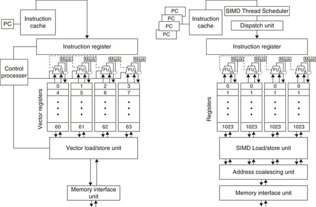
Figure 4.22 A vector processor with four lanes on the left and a multithreaded SIMD Processor of a GPU with four SIMD Lanes on the right. (GPUs typically have 8 to 16 SIMD Lanes.) The control processor supplies scalar operands for scalar-vector operations, increments addressing for unit and non-unit stride accesses to memory, and performs other accounting-type operations. Peak memory performance only occurs in a GPU when the Address Coalescing unit can discover localized addressing. Similarly, peak computational performance occurs when all internal mask bits are set identically. Note that the SIMD Processor has one PC per SIMD thread to help with multithreading.
In reality, there are many more lanes in GPUs, so GPU “chimes” are shorter. While a vector processor might have 2 to 8 lanes and a vector length of, say, 32—making a chime 4 to 16 clock cycles—a multithreaded SIMD Processor might have 8 or 16 lanes. A SIMD thread is 32 elements wide, so a GPU chime would just be 2 or 4 clock cycles. This difference is why we use “SIMD Processor” as the more descriptive term because it is closer to a SIMD design than it is to a traditional vector processor design.
The closest GPU term to a vectorized loop is Grid, and a PTX instruction is the closest to a vector instruction since a SIMD Thread broadcasts a PTX instruction to all SIMD Lanes.
With respect to memory access instructions in the two architectures, all GPU loads are gather instructions and all GPU stores are scatter instructions. If data addresses of CUDA Threads refer to nearby addresses that fall in the same cache/memory block at the same time, the Address Coalescing Unit of the GPU will ensure high memory bandwidth. The explicit unit-stride load and store instructions of vector architectures versus the implicit unit stride of GPU programming is why writing efficient GPU code requires that programmers think in terms of SIMD operations, even though the CUDA programming model looks like MIMD. As CUDA Threads can generate their own addresses, strided as well as gather-scatter, addressing vectors are found in both vector architectures and GPUs.
As we mentioned several times, the two architectures take very different approaches to hiding memory latency. Vector architectures amortize it across all the elements of the vector by having a deeply pipelined access so you pay the latency only once per vector load or store. Hence, vector loads and stores are like a block transfer between memory and the vector registers. In contrast, GPUs hide memory latency using multithreading. (Some researchers are investigating adding multithreading to vector architectures to try to capture the best of both worlds.)
With respect to conditional branch instructions, both architectures implement them using mask registers. Both conditional branch paths occupy time and/or space even when they do not store a result. The difference is that the vector compiler manages mask registers explicitly in software while the GPU hardware and assembler manages them implicitly using branch synchronization markers and an internal stack to save, complement, and restore masks.
As mentioned above, the conditional branch mechanism of GPUs gracefully handles the strip-mining problem of vector architectures. When the vector length is unknown at compile time, the program must calculate the modulo of the application vector length and the maximum vector length and store it in the vector length register. The strip-minded loop then resets the vector length register to the maximum vector length for the rest of the loop. This case is simpler with GPUs since they just iterate the loop until all the SIMD Lanes reach the loop bound. On the last iteration, some SIMD Lanes will be masked off and then restored after the loop completes.
The control processor of a vector computer plays an important role in the execution of vector instructions. It broadcasts operations to all the vector lanes and broadcasts a scalar register value for vector-scalar operations. It also does implicit calculations that are explicit in GPUs, such as automatically incrementing memory addresses for unit-stride and non-unit-stride loads and stores. The control processor is missing in the GPU. The closest analogy is the Thread Block Scheduler, which assigns Thread Blocks (bodies of vector loop) to multithreaded SIMD Processors. The runtime hardware mechanisms in a GPU that both generate addresses and then discover if they are adjacent, which is commonplace in many DLP applications, are likely less power efficient than using a control processor.
The scalar processor in a vector computer executes the scalar instructions of a vector program; that is, it performs operations that would be too slow to do in the vector unit. Although the system processor that is associated with a GPU is the closest analogy to a scalar processor in a vector architecture, the separate address spaces plus transferring over a PCle bus means thousands of clock cycles of overhead to use them together. The scalar processor can be slower than a vector processor for floating-point computations in a vector computer, but not by the same ratio as the system processor versus a multithreaded SIMD Processor (given the overhead).
Hence, each “vector unit” in a GPU must do computations that you would expect to do on a scalar processor in a vector computer. That is, rather than calculate on the system processor and communicate the results, it can be faster to disable all but one SIMD Lane using the predicate registers and built-in masks and do the scalar work with one SIMD Lane. The relatively simple scalar processor in a vector computer is likely to be faster and more power efficient than the GPU solution. If system processors and GPUs become more closely tied together in the future, it will be interesting to see if system processors can play the same role as scalar processors do for vector and Multimedia SIMD architectures.
Similarities and Differences between Multimedia SIMD Computers and GPUs
At a high level, multicore computers with Multimedia SIMD instruction extensions do share similarities with GPUs. Figure 4.23 summarizes the similarities and differences.

Figure 4.23 Similarities and differences between multicore with Multimedia SIMD extensions and recent GPUs.
Both are multiprocessors whose processors use multiple SIMD lanes, although GPUs have more processors and many more lanes. Both use hardware multithreading to improve processor utilization, although GPUs have hardware support for many more threads. Recent innovations in GPUs mean that now both have similar performance ratios between single-precision and double-precision floating-point arithmetic. Both use caches, although GPUs use smaller streaming caches and multicore computers use large multilevel caches that try to contain whole working sets completely. Both use a 64-bit address space, although the physical main memory is much smaller in GPUs. While GPUs support memory protection at the page level, they do not support demand paging.
In addition to the large numerical differences in processors, SIMD lanes, hardware thread support, and cache sizes, there are many architectural differences. The scalar processor and Multimedia SIMD instructions are tightly integrated in traditional computers; they are separated by an I/O bus in GPUs, and they even have separate main memories. The multiple SIMD processors in a GPU use a single address space, but the caches are not coherent as they are in traditional multicore computers. Unlike GPUs, multimedia SIMD instructions do not support gather-scatter memory accesses, which Section 4.7 shows is a significant omission.
Summary
Now that the veil has been lifted, we can see that GPUs are really just multithreaded SIMD processors, although they have more processors, more lanes per processor, and more multithreading hardware than do traditional multicore computers. For example, the Fermi GTX 480 has 15 SIMD processors with 16 lanes per processor and hardware support for 32 SIMD threads. Fermi even embraces instruction-level parallelism by issuing instructions from two SIMD threads to two sets of SIMD lanes. They also have less cache memory—Fermi’s L2 cache is 0.75 megabyte—and it is not coherent with the distant scalar processor.
The CUDA programming model wraps up all these forms of parallelism around a single abstraction, the CUDA Thread. Thus, the CUDA programmer can think of programming thousands of threads, although they are really executing each block of 32 threads on the many lanes of the many SIMD Processors. The CUDA programmer who wants good performance keeps in mind that these threads are blocked and executed 32 at a time and that addresses need to be to adjacent addresses to get good performance from the memory system.
Although we’ve used CUDA and the NVIDIA GPU in this section, rest assured that the same ideas are found in the OpenCL programming language and in GPUs from other companies.
Now that you understand better how GPUs work, we reveal the real jargon. Figures 4.24 and 4.25 match the descriptive terms and definitions of this section with the official CUDA/NVIDIA and AMD terms and definitions. We also include the OpenCL terms. We believe the GPU learning curve is steep in part because of using terms such as “Streaming Multiprocessor” for the SIMD Processor, “Thread Processor” for the SIMD Lane, and “Shared Memory” for Local Memory—especially since Local Memory is not shared between SIMD Processors! We hope that this two-step approach gets you up that curve quicker, even if it’s a bit indirect.

Figure 4.24 Conversion from terms used in this chapter to official NVIDIA/CUDA and AMD jargon. OpenCL names are given in the book definition.

Figure 4.25 Conversion from terms used in this chapter to official NVIDIA/CUDA and AMD jargon. Note that our descriptive terms “Local Memory” and “Private Memory” use the OpenCL terminology. NVIDIA uses SIMT, single-instruction multiple-thread, rather than SIMD, to describe a streaming multiprocessor. SIMT is preferred over SIMD because the per-thread branching and control flow are unlike any SIMD machine.
4.5 Detecting and Enhancing Loop-Level Parallelism
Loops in programs are the fountainhead of many of the types of parallelism we discussed above and in Chapter 5. In this section, we discuss compiler technology for discovering the amount of parallelism that we can exploit in a program as well as hardware support for these compiler techniques. We define precisely when a loop is parallel (or vectorizable), how dependence can prevent a loop from being parallel, and techniques for eliminating some types of dependences. Finding and manipulating loop-level parallelism is critical to exploiting both DLP and TLP, as well as the more aggressive static ILP approaches (e.g., VLIW) that we examine in Appendix H.
Loop-level parallelism is normally analyzed at the source level or close to it, while most analysis of ILP is done once instructions have been generated by the compiler. Loop-level analysis involves determining what dependences exist among the operands in a loop across the iterations of that loop. For now, we will consider only data dependences, which arise when an operand is written at some point and read at a later point. Name dependences also exist and may be removed by the renaming techniques discussed in Chapter 3.
The analysis of loop-level parallelism focuses on determining whether data accesses in later iterations are dependent on data values produced in earlier iterations; such dependence is called a loop-carried dependence. Most of the examples we considered in Chapters 2 and 3 had no loop-carried dependences and, thus, are loop-level parallel. To see that a loop is parallel, let us first look at the source representation:
![]()
In this loop, the two uses of x[i] are dependent, but this dependence is within a single iteration and is not loop carried. There is a loop-carried dependence between successive uses of i in different iterations, but this dependence involves an induction variable that can be easily recognized and eliminated. We saw examples of how to eliminate dependences involving induction variables during loop unrolling in Section 2.2 of Chapter 2, and we will look at additional examples later in this section.
Because finding loop-level parallelism involves recognizing structures such as loops, array references, and induction variable computations, the compiler can do this analysis more easily at or near the source level, as opposed to the machine-code level. Let’s look at a more complex example.
Example
Consider a loop like this one:

Assume that A, B, and C are distinct, nonoverlapping arrays. (In practice, the arrays may sometimes be the same or may overlap. Because the arrays may be passed as parameters to a procedure that includes this loop, determining whether arrays overlap or are identical often requires sophisticated, interprocedural analysis of the program.) What are the data dependences among the statements S1 and S2 in the loop?
Answer
There are two different dependences:
These two dependences are different and have different effects. To see how they differ, let’s assume that only one of these dependences exists at a time. Because the dependence of statement S1 is on an earlier iteration of S1, this dependence is loop carried. This dependence forces successive iterations of this loop to execute in series.
The second dependence (S2 depending on S1) is within an iteration and is not loop carried. Thus, if this were the only dependence, multiple iterations of the loop could execute in parallel, as long as each pair of statements in an iteration were kept in order. We saw this type of dependence in an example in Section 2.2, where unrolling was able to expose the parallelism. These intra-loop dependences are common; for example, a sequence of vector instructions that uses chaining exhibits exactly this sort of dependence.
It is also possible to have a loop-carried dependence that does not prevent parallelism, as the next example shows.
Example
Consider a loop like this one:

What are the dependences between S1 and S2? Is this loop parallel? If not, show how to make it parallel.
Answer
Statement S1 uses the value assigned in the previous iteration by statement S2, so there is a loop-carried dependence between S2 and S1. Despite this loop-carried dependence, this loop can be made parallel. Unlike the earlier loop, this dependence is not circular; neither statement depends on itself, and although S1 depends on S2, S2 does not depend on S1. A loop is parallel if it can be written without a cycle in the dependences, since the absence of a cycle means that the dependences give a partial ordering on the statements.
Although there are no circular dependences in the above loop, it must be transformed to conform to the partial ordering and expose the parallelism. Two observations are critical to this transformation:
These two observations allow us to replace the loop above with the following code sequence:

The dependence between the two statements is no longer loop carried, so that iterations of the loop may be overlapped, provided the statements in each iteration are kept in order.
Our analysis needs to begin by finding all loop-carried dependences. This dependence information is inexact, in the sense that it tells us that such dependence may exist. Consider the following example:

The second reference to A in this example need not be translated to a load instruction, since we know that the value is computed and stored by the previous statement; hence, the second reference to A can simply be a reference to the register into which A was computed. Performing this optimization requires knowing that the two references are always to the same memory address and that there is no intervening access to the same location. Normally, data dependence analysis only tells that one reference may depend on another; a more complex analysis is required to determine that two references must be to the exact same address. In the example above, a simple version of this analysis suffices, since the two references are in the same basic block.
Often loop-carried dependences are in the form of a recurrence. A recurrence occurs when a variable is defined based on the value of that variable in an earlier iteration, often the one immediately preceding, as in the following code fragment:

Detecting a recurrence can be important for two reasons: Some architectures (especially vector computers) have special support for executing recurrences, and, in an ILP context, it may still be possible to exploit a fair amount of parallelism.
Finding Dependences
Clearly, finding the dependences in a program is important both to determine which loops might contain parallelism and to eliminate name dependences. The complexity of dependence analysis arises also because of the presence of arrays and pointers in languages such as C or C++, or pass-by-reference parameter passing in FORTRAN. Since scalar variable references explicitly refer to a name, they can usually be analyzed quite easily with aliasing because of pointers and reference parameters causing some complications and uncertainty in the analysis.
How does the compiler detect dependences in general? Nearly all dependence analysis algorithms work on the assumption that array indices are affine. In simplest terms, a one-dimensional array index is affine if it can be written in the form a × i + b, where a and b are constants and i is the loop index variable. The index of a multidimensional array is affine if the index in each dimension is affine. Sparse array accesses, which typically have the form x[y[i]], are one of the major examples of non-affine accesses.
Determining whether there is a dependence between two references to the same array in a loop is thus equivalent to determining whether two affine functions can have the same value for different indices between the bounds of the loop. For example, suppose we have stored to an array element with index value a × i + b and loaded from the same array with index value c × i + d, where i is the for-loop index variable that runs from m to n. A dependence exists if two conditions hold:
In general, we cannot determine whether dependence exists at compile time. For example, the values of a, b, c, and d may not be known (they could be values in other arrays), making it impossible to tell if a dependence exists. In other cases, the dependence testing may be very expensive but decidable at compile time; for example, the accesses may depend on the iteration indices of multiple nested loops. Many programs, however, contain primarily simple indices where a, b, c, and d are all constants. For these cases, it is possible to devise reasonable compile time tests for dependence.
As an example, a simple and sufficient test for the absence of a dependence is the greatest common divisor (GCD) test. It is based on the observation that if a loop-carried dependence exists, then GCD (c,a) must divide (d − b). (Recall that an integer, x, divides another integer, y, if we get an integer quotient when we do the division y/x and there is no remainder.)

The GCD test is sufficient to guarantee that no dependence exists; however, there are cases where the GCD test succeeds but no dependence exists. This can arise, for example, because the GCD test does not consider the loop bounds.
In general, determining whether a dependence actually exists is NP-complete. In practice, however, many common cases can be analyzed precisely at low cost. Recently, approaches using a hierarchy of exact tests increasing in generality and cost have been shown to be both accurate and efficient. (A test is exact if it precisely determines whether a dependence exists. Although the general case is NP-complete, there exist exact tests for restricted situations that are much cheaper.)
In addition to detecting the presence of a dependence, a compiler wants to classify the type of dependence. This classification allows a compiler to recognize name dependences and eliminate them at compile time by renaming and copying.
Example
The following loop has multiple types of dependences. Find all the true dependences, output dependences, and antidependences, and eliminate the output dependences and antidependences by renaming.

Answer
The following dependences exist among the four statements:
The following version of the loop eliminates these false (or pseudo) dependences.

After the loop, the variable X has been renamed X1. In code that follows the loop, the compiler can simply replace the name X by X1. In this case, renaming does not require an actual copy operation, as it can be done by substituting names or by register allocation. In other cases, however, renaming will require copying.
Dependence analysis is a critical technology for exploiting parallelism, as well as for the transformation-like blocking that Chapter 2 covers. For detecting loop-level parallelism, dependence analysis is the basic tool. Effectively compiling programs for vector computers, SIMD computers, or multiprocessors depends critically on this analysis. The major drawback of dependence analysis is that it applies only under a limited set of circumstances, namely, among references within a single loop nest and using affine index functions. Thus, there are many situations where array-oriented dependence analysis cannot tell us what we want to know; for example, analyzing accesses done with pointers, rather than with array indices can be much harder. (This is one reason why FORTRAN is still preferred over C and C++ for many scientific applications designed for parallel computers.) Similarly, analyzing references across procedure calls is extremely difficult. Thus, while analysis of code written in sequential languages remains important, we also need approaches such as OpenMP and CUDA that write explicitly parallel loops.
Eliminating Dependent Computations
As mentioned above, one of the most important forms of dependent computations is a recurrence. A dot product is a perfect example of a recurrence:
![]()
This loop is not parallel because it has a loop-carried dependence on the variable sum. We can, however, transform it to a set of loops, one of which is completely parallel and the other that can be partly parallel. The first loop will execute the completely parallel portion of this loop. It looks like:
![]()
Notice that sum has been expanded from a scalar into a vector quantity (a transformation called scalar expansion) and that this transformation makes this new loop completely parallel. When we are done, however, we need to do the reduce step, which sums up the elements of the vector. It looks like:
![]()
Although this loop is not parallel, it has a very specific structure called a reduction. Reductions are common in linear algebra and, as we shall see in Chapter 6, they are also a key part of the primary parallelism primitive MapReduce used in warehouse-scale computers. In general, any function can be used as a reduction operator, and common cases include operators such as max and min.
Reductions are sometimes handled by special hardware in a vector and SIMD architecture that allows the reduce step to be done much faster than it could be done in scalar mode. These work by implementing a technique similar to what can be done in a multiprocessor environment. While the general transformation works with any number of processors, suppose for simplicity we have 10 processors. In the first step of reducing the sum, each processor executes the following (with p as the processor number ranging from 0 to 9):
![]()
This loop, which sums up 1000 elements on each of the ten processors, is completely parallel. A simple scalar loop can then complete the summation of the last ten sums. Similar approaches are used in vector and SIMD processors.
It is important to observe that the above transformation relies on associativity of addition. Although arithmetic with unlimited range and precision is associative, computer arithmetic is not associative, for either integer arithmetic, because of limited range, or floating-point arithmetic, because of both range and precision. Thus, using these restructuring techniques can sometimes lead to erroneous behavior, although such occurrences are rare. For this reason, most compilers require that optimizations that rely on associativity be explicitly enabled.
4.6 Crosscutting Issues
Energy and DLP: Slow and Wide versus Fast and Narrow
A fundamental energy advantage of data-level parallel architectures comes from the energy equation in Chapter 1. Since we assume ample data-level parallelism, the performance is the same if we halve the clock rate and double the execution resources: twice the number of lanes for a vector computer, wider registers and ALUs for multimedia SIMD, and more SIMD lanes for GPUs. If we can lower the voltage while dropping the clock rate, we can actually reduce energy as well as the power for the computation while maintaining the same peak performance. Hence, DLP processors tend to have lower clock rates than system processors, which rely on high clock rates for performance (see Section 4.7).
Compared to out-of-order processors, DLP processors can have simpler control logic to launch a large number of operations per clock cycle; for example, the control is identical for all lanes in vector processors, and there is no logic to decide on multiple instruction issue or speculative execution logic. Vector architectures can also make it easier to turn off unused portions of the chip. Each vector instruction explicitly describes all the resources it needs for a number of cycles when the instruction issues.
Banked Memory and Graphics Memory
Section 4.2 noted the importance of substantial memory bandwidth for vector architectures to support unit stride, non-unit stride, and gather-scatter accesses.
To achieve their high performance, GPUs also require substantial memory bandwidth. Special DRAM chips designed just for GPUs, called GDRAM for graphics DRAM, help deliver this bandwidth. GDRAM chips have higher bandwidth often at lower capacity than conventional DRAM chips. To deliver this bandwidth, GDRAM chips are often soldered directly onto the same board as the GPU rather than being placed into DIMM modules that are inserted into slots on a board, as is the case for system memory. DIMM modules allow for much greater capacity and for the system to be upgraded, unlike GDRAM. This limited capacity—about 4 GB in 2011—is in conflict with the goal of running bigger problems, which is a natural use of the increased computational power of GPUs.
To deliver the best possible performance, GPUs try to take into account all the features of GDRAMs. They are typically arranged internally as 4 to 8 banks, with a power of 2 number of rows (typically 16,384) and a power of 2 number of bits per row (typically 8192). Chapter 2 describes the details of DRAM behavior that GPUs try to match.
Given all the potential demands on the GDRAMs from both the computation tasks and the graphics acceleration tasks, the memory system could see a large number of uncorrelated requests. Alas, this diversity hurts memory performance. To cope, the GPU’s memory controller maintains separate queues of traffic bound for different GDRAM banks, waiting until there is enough traffic to justify opening a row and transferring all requested data at once. This delay improves bandwidth but stretches latency, and the controller must ensure that no processing units starve while waiting for data, for otherwise neighboring processors could become idle. Section 4.7 shows that gather-scatter techniques and memory-bank-aware access techniques can deliver substantial increases in performance versus conventional cache-based architectures.
Strided Accesses and TLB Misses
One problem with strided accesses is how they interact with the translation lookaside buffer (TLB) for virtual memory in vector architectures or GPUs. (GPUs use TLBs for memory mapping.) Depending on how the TLB is organized and the size of the array being accessed in memory, it is even possible to get one TLB miss for every access to an element in the array!
4.7 Putting It All Together: Mobile versus Server GPUs and Tesla versus Core i7
Given the popularity of graphics applications, GPUs are now found in both mobile clients as well as traditional servers or heavy-duty desktop computers. Figure 4.26 lists the key characteristics of the NVIDIA Tegra 2 for mobile clients, which is used in the LG Optimus 2X and runs Android OS, and the Fermi GPU for servers. GPU server engineers hope to be able to do live animation within five years after a movie is released. GPU mobile engineers in turn want within five more years that a mobile client can do what a server or game console does today. More concretely, the overarching goal is for the graphics quality of a movie such as Avatar to be achieved in real time on a server GPU in 2015 and on your mobile GPU in 2020.

Figure 4.26 Key features of the GPUs for mobile clients and servers. The Tegra 2 is the reference platform for Android OS and is found in the LG Optimus 2X cell phone.
The NVIDIA Tegra 2 for mobile devices provides both the system processor and the GPU in a single chip using a single physical memory. The system processor is a dual-core ARM Cortex-A9, with each core using out-of-order execution and dual instruction issue. Each core includes the optional floating-point unit.
The GPU has hardware acceleration for programmable pixel shading, programmable vertex and lighting, and 3D graphics, but it does not include the GPU computing features needed to run CUDA or OpenCL programs.
The die size is 57 mm2 (7.5 × 7.5 mm) in a 40 nm TSMC process, and it contains 242 million transistors. It uses 1.5 watts.
The NVIDIA GTX 480 in Figure 4.26 is the first implementation of the Fermi architecture. The clock rate is 1.4 GHz, and it includes 15 SIMD processors. The chip itself has 16, but to improve yield only 15 of the 16 need work for this product. The path to GDDR5 memory is 384 (6 × 64) bits wide, and it interfaces that clock at 1.84 GHz, offering a peak memory bandwidth of 177 GBytes/sec by transferring on both clock edges of double data rate memory. It connects to the host system processor and memory via a PCI Express 2.0 × 16 link, which has a peak bidirectional rate of 12 GBytes/sec.
All physical characteristics of the GTX 480 die are impressively large: It contains 3.0 billion transistors, the die size is 520 mm2 (22.8 × 22.8 mm) in a 40 nm TSMC process, and the typical power is 167 watts. The whole module is 250 watts, which includes the GPU, GDRAMs, fans, power regulators, and so on.
Comparison of a GPU and a MIMD with Multimedia SIMD
A group of Intel researchers published a paper [Lee et al. 2010] comparing a quad-core Intel i7 (see Chapter 3) with multimedia SIMD extensions to the previous generation GPU, the Tesla GTX 280. Figure 4.27 lists the characteristics of the two systems. Both products were purchased in Fall 2009. The Core i7 is in Intel’s 45-nanometer semiconductor technology while the GPU is in TSMC’s 65-nanometer technology. Although it might have been more fair to have a comparison by a neutral party or by both interested parties, the purpose of this section is not to determine how much faster one product is than another, but to try to understand the relative value of features of these two contrasting architecture styles.

Figure 4.27 Intel Core i7-960, NVIDIA GTX 280, and GTX 480 specifications. The rightmost columns show the ratios of GTX 280 and GTX 480 to Core i7. For single-precision SIMD FLOPS on the GTX 280, the higher speed (933) comes from a very rare case of dual issuing of fused multiply-add and multiply. More reasonable is 622 for single fused multiply-adds. Although the case study is between the 280 and i7, we include the 480 to show its relationship to the 280 since it is described in this chapter. Note that these memory bandwidths are higher than in Figure 4.28 because these are DRAM pin bandwidths and those in Figure 4.28 are at the processors as measured by a benchmark program. (From Table 2 in Lee et al. [2010].)
The rooflines of the Core i7 920 and GTX 280 in Figure 4.28 illustrate the differences in the computers. The 920 has a slower clock rate than the 960 (2.66 GHz versus 3.2 GHz), but the rest of the system is the same. Not only does the GTX 280 have much higher memory bandwidth and double-precision floating-point performance, but also its double-precision ridge point is considerably to the left. As mentioned above, it is much easier to hit peak computational performance the further the ridge point of the roofline is to the left. The double-precision ridge point is 0.6 for the GTX 280 versus 2.6 for the Core i7. For single-precision performance, the ridge point moves far to the right, as it’s much harder to hit the roof of single-precision performance because it is so much higher. Note that the arithmetic intensity of the kernel is based on the bytes that go to main memory, not the bytes that go to cache memory. Thus, caching can change the arithmetic intensity of a kernel on a particular computer, presuming that most references really go to the cache. The Rooflines help explain the relative performance in this case study. Note also that this bandwidth is for unit-stride accesses in both architectures. Real gather-scatter addresses that are not coalesced are slower on the GTX 280 and on the Core i7, as we shall see.

Figure 4.28 Roofline model [Williams et al. 2009]. These rooflines show double-precision floating-point performance in the top row and single-precision performance in the bottom row. (The DP FP performance ceiling is also in the bottom row to give perspective.) The Core i7 920 on the left has a peak DP FP performance of 42.66 GFLOP/sec, a SP FP peak of 85.33 GFLOP/sec, and a peak memory bandwidth of 16.4 GBytes/sec. The NVIDIA GTX 280 has a DP FP peak of 78 GFLOP/sec, SP FP peak of 624 GFLOP/sec, and 127 GBytes/sec of memory bandwidth. The dashed vertical line on the left represents an arithmetic intensity of 0.5 FLOP/byte. It is limited by memory bandwidth to no more than 8 DP GFLOP/sec or 8 SP GFLOP/sec on the Core i7. The dashed vertical line to the right has an arithmetic intensity of 4 FLOP/byte. It is limited only computationally to 42.66 DP GFLOP/sec and 64 SP GFLOP/sec on the Core i7 and 78 DP GFLOP/sec and 512 DP GFLOP/sec on the GTX 280. To hit the highest computation rate on the Core i7 you need to use all 4 cores and SSE instructions with an equal number of multiplies and adds. For the GTX 280, you need to use fused multiply-add instructions on all multithreaded SIMD processors. Guz et al. [2009] have an interesting analytic model for these two architectures.
The researchers said that they selected the benchmark programs by analyzing the computational and memory characteristics of four recently proposed benchmark suites and then “formulated the set of throughput computing kernels that capture these characteristics.” Figure 4.29 describes these 14 kernels, and Figure 4.30 shows the performance results, with larger numbers meaning faster.

Figure 4.29 Throughput computing kernel characteristics (from Table 1 in Lee et al. [2010].) The name in parentheses identifies the benchmark name in this section. The authors suggest that code for both machines had equal optimization effort.

Figure 4.30 Raw and relative performance measured for the two platforms. In this study, SAXPY is just used as a measure of memory bandwidth, so the right unit is GBytes/sec and not GFLOP/sec. (Based on Table 3 in [Lee et al. 2010].)
Given that the raw performance specifications of the GTX 280 vary from 2.5× slower (clock rate) to 7.5× faster (cores per chip) while the performance varies from 2.0× slower (Solv) to 15.2× faster (GJK), the Intel researchers explored the reasons for the differences:
It is striking how often weaknesses in the Tesla GTX 280 that were uncovered by kernels selected by Intel researchers were already being addressed in the successor architecture to Tesla: Fermi has faster double-precision floating-point performance, atomic operations, and caches. (In a related study, IBM researchers made the same observation [Bordawekar 2010].) It was also interesting that the gather-scatter support of vector architectures that predate the SIMD instructions by decades was so important to the effective usefulness of these SIMD extensions, which some had predicted before the comparison [Gebis and Patterson 2007] The Intel researchers noted that 6 of the 14 kernels would exploit SIMD better with more efficient gather-scatter support on the Core i7. This study certainly establishes the importance of cache blocking as well. It will be interesting to see if future generations of the multicore and GPU hardware, compilers, and libraries respond with features that improve performance on such kernels.
We hope that there will be more such multicore-GPU comparisons. Note that an important feature missing from this comparison was describing the level of effort to get the results for the two systems. Ideally, future comparisons would release the code used on both systems so that others could recreate the same experiments on different hardware platforms and possibly improve on the results.
4.8 Fallacies and Pitfalls
While data-level parallelism is the easiest form of parallelism after ILP from the programmer’s perspective, and plausibly the easiest from the architect’s perspective, it still has many fallacies and pitfalls.
Fallacy GPUs suffer from being coprocessors
While the split between main memory and GPU memory has disadvantages, there are advantages to being at a distance from the CPU.
For example, PTX exists in part because of the I/O device nature of GPUs. This level of indirection between the compiler and the hardware gives GPU architects much more flexibility than system processor architects. It’s often hard to know in advance whether an architecture innovation will be well supported by compilers and libraries and be important to applications. Sometimes a new mechanism will even prove useful for one or two generations and then fade in importance as the IT world changes. PTX allows GPU architects to try innovations speculatively and drop them in subsequent generations if they disappoint or fade in importance, which encourages experimentation. The justification for inclusion is understandably much higher for system processors—and hence much less experimentation can occur—as distributing binary machine code normally implies that new features must be supported by all future generations of that architecture.
A demonstration of the value of PTX is that the Fermi architecture radically changed the hardware instruction set—from being memory-oriented like x86 to being register-oriented like MIPS as well as doubling the address size to 64 bits—without disrupting the NVIDIA software stack.
Pitfall Concentrating on peak performance in vector architectures and ignoring start-up overhead
Early memory-memory vector processors such as the TI ASC and the CDC STAR-100 had long start-up times. For some vector problems, vectors had to be longer than 100 for the vector code to be faster than the scalar code! On the CYBER 205—derived from the STAR-100—the start-up overhead for DAXPY is 158 clock cycles, which substantially increases the break-even point. If the clock rates of the Cray-1 and the CYBER 205 were identical, the Cray-1 would be faster until the vector length is greater than 64. Because the Cray-1 clock was also faster (even though the 205 was newer), the crossover point was a vector length over 100.
Pitfall Increasing vector performance, without comparable increases in scalar performance
This imbalance was a problem on many early vector processors, and a place where Seymour Cray (the architect of the Cray computers) rewrote the rules. Many of the early vector processors had comparatively slow scalar units (as well as large start-up overheads). Even today, a processor with lower vector performance but better scalar performance can outperform a processor with higher peak vector performance. Good scalar performance keeps down overhead costs (strip mining, for example) and reduces the impact of Amdahl’s law.
A good example of this comes from comparing a fast scalar processor and a vector processor with lower scalar performance. The Livermore FORTRAN kernels are a collection of 24 scientific kernels with varying degrees of vectorization. Figure 4.31 shows the performance of two different processors on this benchmark. Despite the vector processor’s higher peak performance, its low scalar performance makes it slower than a fast scalar processor as measured by the harmonic mean.

Figure 4.31 Performance measurements for the Livermore FORTRAN kernels on two different processors. Both the MIPS M/120-5 and the Stardent-1500 (formerly the Ardent Titan-1) use a 16.7 MHz MIPS R2000 chip for the main CPU. The Stardent-1500 uses its vector unit for scalar FP and has about half the scalar performance (as measured by the minimum rate) of the MIPS M/120-5, which uses the MIPS R2010 FP chip. The vector processor is more than a factor of 2.5× faster for a highly vectorizable loop (maximum rate). However, the lower scalar performance of the Stardent-1500 negates the higher vector performance when total performance is measured by the harmonic mean on all 24 loops.
The flip of this danger today is increasing vector performance—say, by increasing the number of lanes—without increasing scalar performance. Such myopia is another path to an unbalanced computer.
Fallacy You can get good v ector performance without providing memory bandwidth
As we saw with the DAXPY loop and the Roofline model, memory bandwidth is quite important to all SIMD architectures. DAXPY requires 1.5 memory references per floating-point operation, and this ratio is typical of many scientific codes. Even if the floating-point operations took no time, a Cray-1 could not increase the performance of the vector sequence used, since it is memory limited. The Cray-1 performance on Linpack jumped when the compiler used blocking to change the computation so that values could be kept in the vector registers. This approach lowered the number of memory references per FLOP and improved the performance by nearly a factor of two! Thus, the memory bandwidth on the Cray-1 became sufficient for a loop that formerly required more bandwidth.
Fallacy On GPUs, just add more threads if you don’t have enough memory performance
GPUs use many CUDA threads to hide the latency to main memory. If memory accesses are scattered or not correlated among CUDA threads, the memory system will get progressively slower in responding to each individual request. Eventually, even many threads will not cover the latency. For the “more CUDA threads” strategy to work, not only do you need lots of CUDA Threads, but the CUDA threads themselves also must be well behaved in terms of locality of memory accesses.
4.9 Concluding Remarks
Data-level parallelism is increasing in importance for personal mobile devices, given the popularity of applications showing the importance of audio, video, and games on these devices. When combined with an easier to program model than task-level parallelism and potentially better energy efficiency, it’s easy to predict a renaissance for data-level parallelism in this next decade. Indeed, we can already see this emphasis in products, as both GPUs and traditional processors have been increasing the number of SIMD lanes at least as fast as they have been adding processors (see Figure 4.1 on page 263).
Hence, we are seeing system processors take on more of the characteristics of GPUs, and vice versa. One of the biggest differences in performance between conventional processors and GPUs has been for gather-scatter addressing. Traditional vector architectures show how to add such addressing to SIMD instructions, and we expect to see more ideas added from the well-proven vector architectures to SIMD extensions over time.
As we said at the opening of Section 4.4, the GPU question is not simply which architecture is best, but, given the hardware investment to do graphics well, how can it be enhanced to support computation that is more general? Although vector architectures have many advantages on paper, it remains to be proven whether vector architectures can be as good a foundation for graphics as GPUs.
GPU SIMD processors and compilers are still of relatively simple design. Techniques that are more aggressive will likely be introduced over time to increase GPU utilization, especially since GPU computing applications are just starting to be developed. By studying these new programs, GPU designers will surely discover and implement new machine optimizations. One question is whether the scalar processor (or control processor), which serves to save hardware and energy in vector processors, will appear within GPUs.
The Fermi architecture has already included many features found in conventional processors to make GPUs more mainstream, but there are still others necessary to close the gap. Here are a few we expect to be addressed in the near future.
Having covered the many versions of SIMD, the next chapter dives into the realm of MIMD.
4.10 Historical Perspective and References
Section L.6 (available online) features a discussion on the Illiac IV (a representative of the early SIMD architectures) and the Cray-1 (a representative of vector architectures). We also look at multimedia SIMD extensions and the history of GPUs.
Case Study and Exercises by Jason D. Bakos
Case Study: Implementing a Vector Kernel on a Vector Processor and GPU
Concepts illustrated by this case study
MrBayes is a popular and well-known computational biology application for inferring the evolutionary histories among a set of input species based on their multiply-aligned DNA sequence data of length n. MrBayes works by performing a heuristic search over the space of all binary tree topologies for which the inputs are the leaves. In order to evaluate a particular tree, the application must compute an n × 4 conditional likelihood table (named clP) for each interior node. The table is a function of the conditional likelihood tables of the node’s two descendent nodes (clL and clR, single precision floating point) and their associated n × 4 × 4 transition probability tables (tiPL and tiPR, single precision floating point). One of this application’s kernels is the computation of this conditional likelihood table and is shown below:


SUMR.S Fd, Vs Vector Summation Reduction Single Precision:
This instruction performs a summation reduction on a vector register Vs, writing to the sum into scalar register Fd.

Assume the maximum vector length is 64. Is there any way performance can be improved using gather-scatter loads? If so, by how much?

Exercises

Assume that the processor runs at 700 MHz and has a maximum vector length of 64. The load/store unit has a start-up overhead of 15 cycles; the multiply unit, 8 cycles; and the add/subtract unit, 5 cycles.
![]()
A vectorizing compiler might apply a transformation called scalar expansion, which expands dot into a vector and splits the loop such that the multiply can be performed with a vector operation, leaving the reduction as a separate scalar operation:
![]()
As mentioned in Section 4.5, if we allow the floating-point addition to be associative, there are several techniques available for parallelizing the reduction.

Rewrite the loop to meet these guidelines and eliminate the use of the modulo operator. Assume that there are 32 threads per warp and a bank conflict occurs whenever two or more threads from the same warp reference an index whose modulo by 32 are equal.

Assume that dH1, dH2, Hy, Hz, dy, dz, Ca, Cb, and Ex are all single-precision floating-point arrays. Assume IDx is an array of unsigned int.
What is speedup in throughput for each of these improvements?

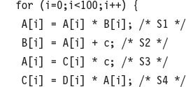

Are there dependences between S1 and S2? Is this loop parallel? If not, show how to make it parallel.
Without considering memory bandwidth, what is the peak single-precision floating-point throughput for this GPU in GLFOP/sec, assuming that all memory latencies can be hidden? Is this throughput sustainable given the memory bandwidth limitation?
After finishing the kernel answer the following questions:
1 This chapter is based on material in Appendix F, “Vector Processors,” by Krste Asanovic, and Appendix G, “Hardware and Software for VLIW and EPIC” from the 4th edition of this book; on material in Appendix A, “Graphics and Computing GPUs,” by John Nickolls and David Kirk, from the 4th edition of Computer Organization and Design; and to a lesser extent on material in “Embracing and Extending 20th-Century Instruction Set Architectures,” by Joe Gebis and David Patterson, IEEE Computer, April 2007.