
Plasma Nanoscience and Nanotechnology
6.1 Plasmas for nanotechnology
6.1.1 Definitions
Nanoscience is defined as a research field that encompasses objects having dimensions smaller than 100 nanometers. Nanoscience addresses basic organization principles of the nanoscopic objects and describes their unique properties. Objects at this scale exhibit very different properties and physics than that of the bulk objects of the same material. At this scale, quantum mechanic effects become very important. Nanotechnology deals with synthesis of nanoscopic objects and devices as well as various applications. Nanoscopic objects could be formed from the precursors in various states (atoms, molecules, clusters, exited states, etc.). Plasma nanoscience and nanotechnology deal with synthesis of nanoparticles from the ionized gas or plasma state.
In general, nanoscience and nanotechnology study nanoscopic objects used across many scientific fields, such as chemistry, biology, physics, materials science, and engineering. By encompassing nanoscale science, engineering, and technology, nanotechnology involves imaging, measuring, modeling, and manipulating matter at this length scale.
Historically, many ideas and concepts behind nanoscience and nanotechnology as they are known today started with a talk entitled “There’s Plenty of Room at the Bottom” by physicist Richard Feynman at an American Physical Society meeting at the California Institute of Technology on December 29, 1959, long before the term nanotechnology was used [1]. In that, now famous talk, Feynman described a process in which scientists would be able to manipulate and control individual atoms and molecules.
This section is devoted to description of the plasma-based nanoscience and nanotechnology, which is emerging as one of the promising field.
6.1.2 Plasma-based synthesis of nanoparticles
Deterministic synthesis of nanoparticles and nanodevices is the most pressing demand of today’s nanotechnology. At the elementary level, this means high fidelity control over the precursor density and energy distribution as well as a high degree of control over precursor position. In this respect, presence of the charged particles allows particle manipulation using electric and magnetic fields. As a result, plasma-based nanoparticle synthesis and fabrication could offer a better degree of controllability in the size, shape, and pattern uniformity as compared to neutral-based process such as chemical vapor deposition (CVD) [2]. An observation made in numerical simulations demonstrates this statement (Figure 6.1). One can see that the nanotips grown on plasma-exposed surfaces (plasma-enhanced CVD) are much taller and sharper than those grown by the CVD process under the same deposition conditions.
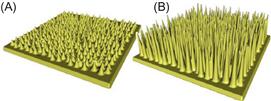
Figure 6.1 Developed carbon nanotip patterns (A) grown by CVD and (B) grown by plasma-enhanced CVD in a plasma with density of about 3.0×10¹⁸ m−3.
Plasma-based techniques were demonstrated to be effective in synthesis of various nanomaterials such as carbon nanotubes (CNTs), nanofibers, graphene, graphene nanoribbons, graphene nanoflakes, nanodiamond and related carbon-based nanostructures; metal, silicon, and other inorganic nanoparticles and nanostructures; soft organic nanomaterials; nanobiomaterials; biological objects and nanoscale plasma etching [3]. To this end, various types of plasmas and plasma reactor systems are utilized in nanotechnology, including low-temperature nonequilibrium plasmas at low and high pressures, thermal plasmas, high-pressure microplasmas, plasmas in liquids and plasma–liquid interactions, high-energy-density plasmas, and ionized physical vapor deposition to name just a few.
6.1.3 Synthesis of carbon nanoparticles
Carbon is one of the few elements known from antiquity and the one that is mostly used nowadays. There are several allotropes of carbon in the world, which can be categorized by dimensions, such as diamond and graphite in three dimensions, graphene in two dimensions, CNTs in one dimension, and fullerene in zero dimension. Carbon with sp3 hybridization will form a tetrahedral lattice, thus giving rise to diamond. Carbon with sp2 hybridization may form graphite, graphene, CNT, or fullerene, depending on the conditions of their formation. Different structures and hybridizations of carbon atoms can determine the unique properties of each carbon allotropes.
Among possible forms of carbon, CNT and graphene attracted significant interest nowadays. CNT was first discovered in carbon deposits by the arc-discharge method by Iijima in 1991 [4], and the advance of graphene appears when Novoselov et al. [5] were able to extract it from bulk graphite by micromechanical cleavage or the Scotch tape approach in 2004. CNTs have unique structures with cylindrical walls of carbon. According to the number of wall layers, CNT can be categorized as single-walled carbon nanotubes (SWCNTs) and multiwalled carbon nanotubes (MWCNTs), while graphene is one-atom-thick hexagonal-lattice planar carbon layer.
Most SWCNTs have a diameter of around few nanometers, with a tube length that could be millions of times longer. SWCNT can be formed by rolling up a one-layer graphene into a cylinder. The way the graphene sheet is wrapped is represented by a pair of indices (n,m) [6]. The integers of n and m denote the number of unit vectors along two directions in the honeycomb crystal lattice of graphene shown in Figure 6.2. The (n,m) nanotube naming scheme is a vector (Ch) in an infinite graphene sheet that describes how to “roll up” the graphene sheet to make the nanotube as shown in Figure 6.2. An SWCNT can be imagined as graphene sheet rolled at a certain chiral angle with respect to a plane perpendicular to the tube’s long axis. Consequently, SWCNT can be defined by its diameter and chiral angle. The chiral angle can range from 0° to 30°. The SWCNT with index m=0 are named zigzag nanotubes, and the SWCNT with index n=m are called armchair nanotubes. The electrical property of SWCNT is determined by the indices of n and m. If the difference of indices n and m is integral multiple of three, the SWCNTs have metallic properties. The others are semiconducting materials. It will be shown below that various synthesis techniques produce both metallic and semiconductor nanotubes.

Figure 6.2 The (n,m) nanotube naming scheme can be thought of as a vector (Ch) in an infinite graphene sheet that describes how to “roll up” the graphene sheet to make the nanotube. T denotes the tube axis, and a1 and a2 are the unit vectors of graphene in real space.
The unique structures of SWCNT and graphene lead to excellent mechanical, electrical, and thermal properties. SWCNT and graphene appear to be one of the strongest and stiffest materials in terms of Young’s modulus and tensile strength. This strength results from the covalent sp2 bonds formed between the individual carbon atoms. The Young’s modulus of SWCNT and graphene can reach over 1 TPa, which is tens of times higher than that of aluminum [7]. The recent measurements have shown that graphene has a breaking strength which is 200 times greater than steel [8]. Metallic SWCNT can carry an electric current density of 4×10⁹ A/cm2 in theory, which is more than 1000 times greater than those of metals such as copper [9]. Intrinsic graphene is a semimetal or zero-gap semiconductor. Experimental results from transport measurements show that graphene has remarkable electron mobility at room temperature, with reported values in excess of 15,000 cm2/V/s. The corresponding resistivity of the graphene sheet would be 10−6 Ω cm, which is less than the resistivity of silver [10]. SWCNTs have the thermal conductivity of 300 W/(mK) in axial direction. The measurement by a noncontact optical technique demonstrated that the near-room temperature thermal conductivity of graphene was measured to be between (4.84±0.44)×103 and (5.30±0.48)×103 W/(mK) [11], which is significantly higher than that of SWNT.
6.1.3.1 Carbon nanotubes
CNTs are tubular carbon-based structures that are produced from graphitic carbon. Since their discovery, an interest in CNTs has been stimulated by their unique mechanical, thermal, and electrical properties, and various potential applications that exploit these properties, such as field-emission displays [12,13], nanoelectronics [14], hydrogen storage [15], and chemical gas sensors [16]. SWNTs have the greatest stiffness, both in tension and bending [17]. The combination of stiffness and toughness makes single-wall nanotubes (SWNTs) the strongest known fibers. Thus one of the important applications of SWNTs is creation of new materials. Continuum mechanics calculations have shown that SWNTs are among the strongest tubular tensile members available [18]. Several applications that purport to exploit the remarkable mechanical, electrical, and thermal properties of SWNT have been investigated. While the preponderance of applications involving nanotubes are in fields that can be broadly categorized as “life sciences,” real challenges associate with making practical, useful materials of large amounts with superior and unusual mechanical, electrical, and thermal properties.
Several techniques have been developed for CNT synthesis such as arc-discharge, chemical vapor deposition, and laser ablation [19,20]. A progress in arc-discharge SWNT synthesis was motivated by Journet et al. [21] who showed that the SWNTs can be efficiently produced by this technique. The use of anodic arc for CNT synthesis is based on ablation of the anode material and deposition of the ablated material on the cathode. Two different textures and morphologies can be observed in the cathode deposit: the gray outer shell and dark-soft inner core deposit. MWNTs as well as graphitic particles are found typically in the inner core [22]. SWNTs produced by the anodic arc discharge are found in a “collaret” around the cathode deposit, cloth-like soot suspended in the chamber walls, and the weblike structure suspended between cathode and walls [22]. MWNTs and SWNTs produced in arc discharge are dependent on gas background and arc conditions [23,24]. In the He–Ar mixture, it was found that the argon mole fraction affects the SWNT diameter [25], while SWNT diameter was found to be fairly independent of pressure in the pure helium environment [26]. In addition to SWNT diameter, two other parameters are important for SWNT applications, namely chirality and aspect ratio. The chiral angle (as defined at Figure 6.2) determines whether SWNT has metallic or semiconductor electrical conductivity [27]. Some challenges regarding control of the SWNTs chirality and radius were reported [26,28,29]. The issues related to large-scale and high-purity synthesis of SWNT by arc discharge are very important objectives nowadays [30–34].
Among several methods for preparing CNTs, arc discharge is the most practical one for scientific and technological purposes due to the number of advantages in comparison with other techniques. Firstly, arc-discharge method yields highly graphitized tubes with very small defects, because the manufacturing process occurs at a very high temperature (which is about 1200–1500 K, see next two sections) and arc-grown SWNTs demonstrate the highest time of emission capability degradation than those produced by other techniques [35]. Secondly, nanotubes produced in arc usually demonstrate a high flexibility, thus eventually providing higher strength characteristics [36].
The lack of control of the SWNT growth in arc is the main disadvantage of the arc-discharge technique for nanotube. The controllability and flexibility of the arc-plasma-based process may be significantly improved by the use of a magnetic field, which strongly influences the plasma parameters [37]. It was shown that the high-purity multiwall nanotubes (MWNTs) can be grown in the magnetically enhanced arc discharge [38]. It was also demonstrated that the use of the magnetic-field-enhanced arc discharge is very promising for the production of the long SWNTs [39].
SWNTs produced in the arc has aspect ratios typically in the range of 100–1000 [24,39], while there is a tremendous interest in production of ultralong SWNTs (with aspect ratio greater than 105) which will enable new types of Micro-elecro-mechanical and nano-electromechanical (MEMS/NEMS) systems, such as microelectric motors, and can act as a nanoconducting cable [40]. In addition, it was demonstrated that the thermal conductivity of an individual SWNTs increases with length [41], thus making ultralong SWNTs an ideal structure for thermal control.
6.1.3.2 Graphene
Graphene is a one-atom-thick planar sheet of sp2-bonded carbon atoms that are densely packed in a honeycomb crystal lattice [42]. This new material, which combines aspects of semiconductors and metals, could be a leading candidate to replace silicon in applications ranging from high-speed computer chips to biochemical sensors. Large-area graphene films are of enormous interest for electronic and optical applications, namely, their potential was recently demonstrated for field effect transistors (FETs) [43–48] (and in particular for transistors operating at GHz frequencies [49]) and for conductive films on transparent plastic electrodes required for development of concept of flexible and stretchable electronics [50–53].
Single-layer graphene was first synthesized using regular Scotch tape by mechanical exfoliation of layers from bulk graphite [42,54,55], and its creators were awarded by Nobel Prize in Physics for 2012 “for groundbreaking experiments regarding the two-dimensional (2D) material graphene” [56]. Since the method utilized originally by Geim and Novoselov is extremely expensive and characterized by low output, a very active search for more efficient ways of graphene synthesis was facilitated. Among other methods created in following years, one can mention epitaxial growth on SiC, CVD, and colloidal suspensions [45,57–62]. Generally, these methods allow synthesizing two types of the graphene, namely large-area pristine graphene films (i.e., graphene films on Si wafers) and micron-sized graphene platelets (bulk graphene).
The first type of graphene, namely large-area uniform graphene films, is synthesized using epitaxial growth and CVD, and being applied in ultrahigh-speed, low-power graphene-channel FETs, and transparent electrodes [45,63–66]. The graphene films are being first synthesized on the hot metal substrates and then being transferred to desired substrate, e.g., Si wafer or transparent electrode. Currently the main challenges in this field are creation of high-quality continuous and uniform graphene films in CVD process (greater than 8 inches in diameter), and reduction of damages to the graphene film at its transfer [45,63]. Currently there are two widely recognized and well-studied mechanisms of CVD synthesis of graphene. First mechanism is dominant when materials characterized by high solubility of carbon are utilized as a growth substrate, e.g., Ni [52,66]. In this case, the carbon atoms dissolve in the substrate material first and then precipitate on the substrate surface during the substrate’s cooling. These precipitated atoms form graphene film on the substrate surface. Such grown graphene films are usually limited to the grain size of substrate and contains several layers. Second mechanism of graphene growth is employed when materials characterized by low solubility of carbon are utilized for the growth substrate, e.g., Cu [45]. As proposed by Ruoff et al. [45], the graphene growth is surface catalyzed in this case. It was shown that synthesis on Cu substrates is basically self-limited on production of single-layer graphene film of extraordinary quality. Various conditions of the growth substrate were shown to have significant impact on the properties of the final graphene film. Indeed, the crystal structure of the substrate plays an important role in quality of graphene films grown on that substrate and Cu(111) was indicated to yield best quality uniform, monolayer graphene growth [64]. It was shown that degree of substrate polishing changes the homogeneity and electronic transport properties of the grown graphene film and recommendation to utilize the electropolished metal surfaces was made [65].
The second type of graphene, the bulk graphene (graphene platelets, flakes), is usually characterized by several layers (with thickness of about 2–20 nm) graphene pieces having characteristic sizes of about microns. The main application of bulk graphene is electrochemical energy storage devices including ultracapacitors and fuel cells. Currently, the main method for synthesis of bulk graphene is chemical exfoliation, where chemicals are utilized to separate the graphene sheets from the piece of graphite. Current production capability are quite limited and estimated to be around several tens of tons of material annually worldwide [67].
Application of plasmas is a well-known tool to improve properties of the CVD grown films and it makes up the vast category of various plasma-enhanced and plasma-assisted CVD techniques [67,68]. The benefits of the plasma-enhanced CVD techniques are resulted from significant enhancement of the reactivity of species involved in synthesis by means of plasmas. In particular, this approach allows significantly reducing the synthesis temperature (usually to about 300°C), improving adhesion of the films to the substrate and providing higher deposition rates [69,70]. Potential utilization of plasmas in graphene synthesis was recently demonstrated by showing that temperature of synthesis can be reduced by several hundred degrees centigrade from about 1000°C at conventional CVD to about 500–650°C in plasma-enhanced CVD [71,69].
Recently, a new method of graphene synthesis in magnetically controlled anodic arc discharge was discovered [70]. Method utilizes pure carbon vapor ablation from the solid carbon electrode by means of arc discharge in the atmosphere of helium and its following delivery to the heated growth substrate. Preliminary studies demonstrated that a few-layer graphene of superior quality can be synthesized with high efficiency in this plasma-assisted process.
6.1.4 Controlled synthesis of carbon nanostructures in arc plasmas: theoretical premise
Several models of a cathodic carbon arc were developed in past dealing with electrode phenomena [72–74] or interelectrode plasma [75]. A 1D model (in axial direction) of the SWNT formation was developed and the SWNT growth rate in an anodic arc discharge was calculated [76]. According to the existed model predictions, the nanotube formation occurs in the region of relatively small plasma temperature (1300–1800 K [77]) where carbon reacts to form large molecules and clusters. No detailed model for relationship between the discharge parameters and SWNT formation was developed as mentioned in a review paper [78]. A model of SWNT interaction with discharge plasma and SWNT formation in the cathode region (collaret) was developed [79]. It was shown that under certain conditions, SWNT can be deposited on the cathode surface. This process depends on SWNT charging in the arc plasma. In turn, the charging phenomena depend on the electron temperature.
Gamaly and Ebbesen [80] proposed that the bimodal carbon velocity distribution (ions with drift velocity and isotropic neutrals) determines the nanotube creation process near the cathode. They suggested that isotropic distribution leads to fullerene formation, while directed flux results in nanotubes. Iijima et al. [81] proposed an open-ended growth model. In this model, carbon atoms and small carbon clusters add on to the reactive dangling bonds at the edges of the open-ended nanotubes. Other researchers argue that CNTs are elongated by electrostatic forces along the electric field near the cathode [82,83]. However, it seems like a high-resolution transmission electron microscopy (TEM) analysis does not support this hypothesis. Alternatively, a two-step growth model has been proposed [84]. According to this model, different carbon structures are formed first. Then, during the cooling process, the graphitization occurs from the surface toward the interior of the assemblies. Several workers developed a growth model of SWNT explaining the root growth of nanotube bundles emerging from catalyst particles [85]. These models include a catalyst phase diagram of carbon metal. The investigation of mechanism for the catalytic synthesis methods of CNTs in arc plasma is still subject to ongoing research. The vapor–liquid–solid (VLS) mechanism was first proposed by Wagner and Ellis and can be utilized to demonstrate the growth model of SWCNT [86]. According to the VLS framework, Ding et al. [87] simulated the nucleation processes of SWCNT associated with catalyst particles by molecular dynamics method, presenting the dependent relationship between diameters of SWCNT and catalyst particles theoretically. Based on the analysis of diffusion model of carbon atom and calculation by Monte Carlo technique, Keidar et al. [88] also demonstrated that the SWCNT diameter is determined by the size of the molten catalyst core in arc discharge. Chiang and Sankaran [89] reported the very important experimental results suggesting that the variation of the element composition of NixFe1-x catalyst particles strongly affects the SWCNT chirality. The link between the composition-dependent catalyst structure and the chirality of SWCNT would improve the in situ controllability of SWCNT synthesis. The results indicate the important role of the catalyst particles in the SWCNT synthesis.
6.1.4.1 SWNT interaction with arc plasma
In this section, a simple model of SWNT interactions with arc plasma and predictions based on this model will be described.
Typically in the interelectrode gap of the arc-discharge plasma, temperature varies from about 5000 K in the center of the channel down to 1000 K at the periphery [90]. Probability of atomic collisions and therefore nanotube seed formation is higher in the center of the interelectrode gap, i.e., in the region with highest carbon atoms and ions density. Recall that SWNT seeds formed in the plasma are subject to interaction with plasma particles that include charge, momentum, and energy transfer. As a result of these interactions, high heat fluxes may lead to overheating and preventing formation of the stable nanostructures. Thus, the nanotube formation occurs in the region of relatively small plasma temperature (1300–1800 K) where carbon reacts to form large molecules and clusters as will be shown in the following. Although the mechanism of the formation and growth of SWNTs in an arc discharge was studied for a decade [30], location of the region in arc discharge in which SWNT synthesis occurs and the temperature range favorable for SWNT growth remains unclear. According to previous work [30,45], the nanotube formation occurs on the periphery of an arc column at a moderate temperature range of 1200–1800 K. Other studies suggested that it is the cathode sheath adjacent to hot arc column (~5000 K) is the arc region where the nanotube growth occurs [78,91–93]. Recall that in the cathode sheath region, the temperature might be well above the reported critical temperatures of thermal stability of the nanotubes. In this respect, a question about possible CNT growth in cathode sheath region remains open. Moreover, there are no consistent data on the thermal stability of SWNT in the arc discharge, including the temperature ranges of SWNT synthesis and destruction. Thermal stability of SWNTs produced in helium arc was studied [94]. Using a furnace, temperature conditions closely resembling the natural conditions of SWNT growth in an arc were created. Based on these experimental data, it can be concluded that SWNT produced by an anodic arc discharge and collected in the web area outside the arc plasma most likely originated from the arc-discharge peripheral region, i.e., plasma–gas interface.
Let us calculate the residence time of SWNT cluster in the growth region. Carbon clusters diffuse with diffusion coefficient DSWNT from the region of origin without any chemical reactions [95]. In the diffusion approximation, one can determine the diffusion coefficient of carbon clusters and SWNT as follows [95]
![]() (6.1)
(6.1)
where mSWNT and mHe are SWNT and He molecular masses, respectively, T is the plasma temperature, p is the pressure, and dSWNT and dHe are effective diameters of the SWNT seed and He molecule, respectively. In this formulation, the radial diffusion velocity of SWNT seed can be estimated as VSWNT~DSWNT/Ra, where Ra is the anode radius, which is the characteristic dimension of the plasma region. In addition, an initial SWNT velocity can be estimated from experimental measurements and it is about 0.01–0.5 m/s.
The charge transfer from the plasma to SWNT is due to electron and ion fluxes to SWNT seed and due to thermoionic emission from the SWNT:
![]() (6.2)
(6.2)
where QSWNT is SWNT charge, Ii, Ie, Iem are ion, electron, and thermoionic current, respectively. The electron current is given by Ie=Sje, where S is SWNT surface area and je is the electron current density. The electron current density absorbed by SWNT depends upon SWNT potential with respect to the surrounding plasma: je=jeo exp(−eφSWNT/kT) if φSWNT<0 and je=jeo exp(1+eφSWNT/kT) in the opposite case, where jeo is the electron thermal current density, φSWNT is the SWNT potential with respect to the plasma. The ion current density at the SWNT surface is given by ji=jio(1+α) if α≥0 and ji=jio if −1<α<0 and ji=0 if α<−1, where α=−2eφSWNT/miVi2 and jio=eneVi is the ion current density in the plasma and Vi is the ion velocity.
The current of thermoionic emission is given by Richardson–Duschman equation:
![]() (6.3)
(6.3)
where Φ is the work function and Ts is the SWNT temperature.
Following Ref. [96], the electric capacitance of the cylindrical particle is calculated as C=4πεo(L/ln(2L/a)), where L is SWNT length and a is the SWNT radius (a=1.4 nm, [92]). The capacitance does not depend on the inner radius of SWNT since it is calculated between the SWNT and the surrounding plasma. In addition, we take into account that SWNT is a conductor (having either metallic or semiconductor properties), thus SWNT charge is equal: QSWNT=CφSWNT.
SWNT growth rate is determined by carbon atoms and ions precipitation to the nanotube surface and chemical reactions, which depends on the density of carbon species in the vicinity of SWNT and the electron temperature. It is assumed that influx of carbon ions and atoms to SWNT causes an increase in SWNT length. We further assume that growing SWNT has C–C spacing of about 1.4 A° [92]. Flux of the carbon atoms to the SWNT surface can be calculated as follows:
![]() (6.4)
(6.4)
SWNT interaction with plasma in the interelectrode region leads to momentum transfer, which can be accounted as follows:
![]() (6.5)
(6.5)
where FD is the drag force, FD=ρdSWNT(Vi−VSWNT)2, ρ is the plasma density, and E is the electric field in the region of SWNT formation. Equation (6.5) is supplemented by equation for SWNT trajectory: (dr/dt)=VSWNT. Initial velocity of SWNT, VSWNT(r=0) is calculated from Eq. (6.1). System of equations (6.2–6.5) was solved to calculate SWNT trajectory in arc-discharge plasma and SWNT growth. These results are shown in Figure 6.4.
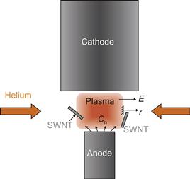
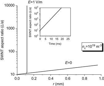
Figure 6.4 SWNT aspect ratio as a function of distance with electric field as a parameter. Insert shows SWNT aspect ration as a function of residence time.
As it is mentioned above, one possibility to affect SWNT growth in the SWNT formation region is to apply an electric field. Due to the fact that SWNT accumulates charge in course of interaction with plasma, it is expected that this electric field may affect SWNT motion. In fact, simulations show that the electric field in the SWNT formation region has strong effect on SWNT motion. SWNT relative length (aspect ratio) is shown in Figure 6.4 with electric field in the SWNT growth region as a parameter. It can be seen that a relatively small electric field significantly affects SWNT growth and leads to a large SWNT aspect ratio in comparison to zero electric field case. This is due to trapping of SWNT in region of the preferable growth. In the enlarged section of Figure 6.4, one can see time evolution of SWNT charge and SWNT aspect ratio.
6.2 Magnetically enhanced synthesis of nanostructures in plasmas
6.2.1 Arc-discharge plasma system for synthesis of SWNT
A typical arc-discharge system consists of anode–cathode assembly installed in a stainless steel flanged chamber capped at both ends as shown in Figure 6.5. The arc discharge is sustained with a constant power supply, using a feedback connected to the linear drive of the anode and the power supply generating the arc. Linear drive allows to keep constant interlectrode gap of about 1 mm during the arcing time. The anode hole is packed with various metal catalysts. Quanta sizing and microscope examinations of arc-discharge products for equal arc runtime has revealed that the catalyst combination yielding the largest amount of nanotubes was Y–Ni in a 1–4 ratio [91]. The nanotube samples are typically produced at constant helium pressures ranging from 500 to 700 Torr and arc current ranging between 70 and 80 A. Magnetic field can be used to enhance arc-discharge technique. Schematically application of a nonuniform magnetic field is shown in Figure 6.6. Photos show that magnetic field modifies arc discharge. Magnetic field leads to formation of a plasma jet that will be describe below.


6.2.2 Synthesis of SWCNTs in a magnetic field
Permanent magnets (5×5×2.5) cm3 with different strengths were used to create and vary the strength of a nearly axial magnetic field in the discharge gap of about 0.5 cm as shown schematically in Figure 6.6. Magnetic field varies in the range of 0.2–2 kG. Samples with SWCNTs collected from locations were subsequently analyzed in the solid state with SEM and Raman spectroscopy, and postprocessing into aqueous dispersion by ultraviolet–visible–near infrared (UV–Vis–NIR) and PL spectroscopy techniques.
Collected samples were analyzed under SEM and the length distribution of individual SWNT was measured from SEM images. SEM data indicate that the presence of a magnetic field makes a significant difference in the average length of the SWNTs produced by the arc discharge as shown in Figure 6.7. Typical SEM image used for length measurements is shown in the inset in Figure 6.7. It should be pointed out that in many cases, it was confirmed that we measured length of a single nanotube, while in other cases we refered to an image of SWNT bundle. Left inset shows a typical SEM image used for length measurements; right inset shows the TEM image of the SWNT and bundle of SWNT. TEM image also indicates that SWNTs in a bundle have the same length. Of the entire measurements of SWNT length taken without the magnetic field, 50% were under 600 nm and 90% were under 1300 nm; while 50% of the measurements taken from samples with the magnetic field were under 1100 nm and 90% were under 2600 nm. Thus, the presence of the magnetic field seemingly doubles the length of SWNTs produced [39].
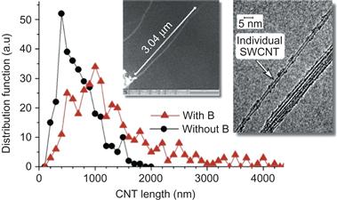
Figure 6.7 Comparison of the SWCNTs lengths distribution with and without magnetic field applied to the arc discharge. Inset shows a typical SEM image used for length measurements. Left inset shows a typical SEM image used for length measurements; right inset shows the TEM image of the single SWNT and a bundle of SWNTs. Source: Reprinted with permission from Ref. [39]. Copyright (2008) by American Institute of Physics.
A mathematical model describing the very complicated problem of the SWNT formation in arc plasma was developed [39,78,79,97,98]. It has been shown that the electrical charges influence the growth of nanostructures [2,99]. In the following, we outline the principle points of these models to explain the SWCNT length increase in the strong magnetic-field-enhanced arc plasmas. The detailed description of the SWCNT growth will be presented in the next section.
A nanotube immersed in the plasma accumulates an electric charge on its surface and eventually encloses by the sheath which thickness can be estimated as ![]() where ε0 is the dielectric constant, Te is the electron temperature, np is the plasma density, e is the electron charge, and γ is a constant in the range of 1–5 [100]. In the sheath, there is an uncompensated electric charge which induced an electric field between the plasma bulk and the SWNT surface. In the calculations considered, it was assumed a maximum SWNT length of 5 μm that is in accordance with experimental data (Figure 6.7). Thus, for the typical plasma density (1017–1018 m−3) and electron temperature (up to 1 eV) in the arc plasma, the sheath thickness is in the range of 15–25 μm that significantly exceeds the SWNT length. While magnetic field can affect the sheath width [101], it does not affect the current collection and thus SWCNT growth. During the process of SWNT formation, the orientation of the nanotube is chaotic and changing in time, so the magnetic field cannot significantly decrease the electron current to the SWNT surface. As a result, the influence of the magnetic field on the sheath is moderate in this case.
where ε0 is the dielectric constant, Te is the electron temperature, np is the plasma density, e is the electron charge, and γ is a constant in the range of 1–5 [100]. In the sheath, there is an uncompensated electric charge which induced an electric field between the plasma bulk and the SWNT surface. In the calculations considered, it was assumed a maximum SWNT length of 5 μm that is in accordance with experimental data (Figure 6.7). Thus, for the typical plasma density (1017–1018 m−3) and electron temperature (up to 1 eV) in the arc plasma, the sheath thickness is in the range of 15–25 μm that significantly exceeds the SWNT length. While magnetic field can affect the sheath width [101], it does not affect the current collection and thus SWCNT growth. During the process of SWNT formation, the orientation of the nanotube is chaotic and changing in time, so the magnetic field cannot significantly decrease the electron current to the SWNT surface. As a result, the influence of the magnetic field on the sheath is moderate in this case.
In the sheath around SWNT, the ion motion is determined by the electrical field between SWNT and plasma bulk. The electric field is described by the Poisson equation for the electric potential Δφ=ρe/ε0, where ρe is the density of electrical charge in the sheath. As a boundary condition for the Poisson equation, an equipotentiality of the entire SWNT surface was assumed, i.e., φ(x,r,α)|(x,R,α)=ΨSWNT, where R is the SWNT radius. Ions enter the sheath with the Bohm velocity ![]() where mi is the ion mass. An ion trajectory in the sheath can be obtained by integrating a motion equation. More details on the electric field and ion motion influence on nanostructures can be found elsewhere [102,103].
where mi is the ion mass. An ion trajectory in the sheath can be obtained by integrating a motion equation. More details on the electric field and ion motion influence on nanostructures can be found elsewhere [102,103].
Here, the following scenario of the SWNT growth in a plasma was implemented. It was assumed that the SWNT grow on the partially molten metal catalyst particle supplied to the plasma from ablated electrode. In plasma, the metal catalyst particle is a subject to the additional heating and ablation, which reduce the catalyst size, and then condition and molten the external layer creating a liquid shell. The carbon atom flux gets to the catalyst surface, diffuse through it, and eventually incorporate into the SWNT structure. An ion flux supplies carbon atoms to the SWNT and catalyst. Upon recombination, carbon adatoms migrate about the SWNT surface, eventually reach the molten catalyst shell or reevaporate to the plasma bulk (Figure 6.8). Today, the two main growth scenarios are mostly accepted: the VLS [104] and solid–liquid–solid (SLS) [105]. Both scenarios involve the carbon atom diffusion in the metal catalyst particle, and thus the process of the carbon supply to the external catalyst surface is a decisive factor that determines the SWNT growth kinetics. To calculate the carbon supply to the catalyst surface, we implemented a diffusion model which was used for simulation of the diffusion-driven growth of carbon nanostructures on surface [106]. For the ion motion calculations, a Monte Carlo technique to obtain an ion flux distribution over the SWNT–catalyst surface was used. The diffusion model is used to calculate adatom migration about SWNT surface and the carbon atoms diffusion in the molten catalyst [107].

Figure 6.8 Growth of SWNT on molten metal catalyst particle in plasma. Carbon flux from plasma is nonuniformly distributed about SWNT and catalyst particle surface. Carbon adatoms diffuse to the catalyst end, and then incorporate into SWNT structure through molten catalyst shell. Source: Reprinted with permission from Ref. [39]. Copyright (2008) by American Institute of Physics.
Obtained ion flux distributions over the nanotube were used for simulation of the SWNT growth rates η (μm×s−1). The results of the calculations are shown in Figure 6.9, with the plasma density as a parameter. We should point out that the SWNT growth rate strongly decreases with the SWNT length and increases with the plasma density. Let us try to interpret the results shown in Figure 6.9. Note that formation of new layers is not considered here; thus, the growth rate of the nanotube depends only on the total influx of the carbon atoms to the surface of catalyst particle, which in turn depends on the total carbon influx to the SWNT and catalyst surfaces, as well as on the influx distribution over the SWNT and catalyst. When an SWNT is short, its growth rate is determined by the total carbon influx and the adaom migration kinetics. An essential part of the carbon atoms gets into the catalyst shell and participate in the SWNT growth. With the SWNT length increasing, the carbon flux to catalyst decreases due to increased carbon loss by evaporation, thus causing the decrease in the SWNT growth rate.

Figure 6.9 Dependence of SWNT growth rate η on SWNT length with plasma density as a parameter. SWNT diameter is 2 nm, catalyst particle diameter is 10 nm. The graph shows strong decrease of SWNT growth rate with the SWNT length. Source: Reprinted with permission from Ref. [39]. Copyright (2008) by American Institute of Physics.
6.2.3 Effect of magnetic field on SWNT chirality
Since the discovery of SWCNTs [4], significant efforts have been directed toward attempts to synthesize SWCNTs of controlled chiral angle as discussed in Section 6.1. In particular, interest in chirality control is driven by the strict requirement to have a narrow distribution of SWCNT diameters, or a small number of chiralities, for enabling nanoelectronic applications [108–110]. Recent works indicate that one of the key parameters for SWCNT chirality control is the initial characteristics of catalyst particle [89,111]. For CD techniques, Li et al. [111] demonstrated that changing the size of their Co-MCM-41 catalyst particle (by altering the synthesis temperature through the range of 550–950 °C) allows for control of the produced SWCNT diameters over the range from 0.6 to 2 nm. Chiang and Sankaran [89] reported that varying the composition of NixFe1−x catalyst particle strongly affects distribution of produced SWCNT chiralities, namely a decrease of x leads to narrower distribution of produced chiralities and a decrease in the mean SWCNT diameter. However, fine control of the chirality distribution through manipulation of the catalyst has proven to be highly demanding, and so alternative techniques for shaping the distribution during the production process are desirable.
Below tuning of the distribution of produced SWCNTs for the anodic arc production method using an applied magnetic field is described. As it was mentioned above, SWCNTs synthesized in anodic arc have properties superior to those produced by CVD, including on the typical measures for quality of nanotubes (smaller defects, higher flexibility and strength) as well as a significantly higher production rate and should thus be more advantageous for practical applications [78,112–114].
Recently, different methods for control of anodic arc synthesis have been reported. It was shown that the anode composition and structure [115], background gas composition and pressure [25,116], and electric field [117] affect the production yield, diameter range, and aspect ratio of the synthesized SWCNTs. Particularly significant progress in control of arc synthesis was demonstrated using the application of external magnetic fields to the arc [39,118]; this magnetically enhanced discharge was demonstrated to be able to control the aspect ratio of SWCNTs [39]. Nanotubes synthesized in magnetically enhanced arc were two times longer than those produced without magnetic field. By changing the strength of the applied static magnetic field, the diameter distribution of the arc product can be controlled as shown schematically in Figure 6.6. The SWCNT samples synthesized at different magnetic fields were analyzed using scanning electron microscopy (SEM), photoluminescence (PL), UV–Vis–NIR absorbance and Raman spectroscopy.
Produced materials were analyzed both as -produced and as an aqueous dispersion. Figure 6.10A shows Raman spectra and SEM images of the as-produced samples (not purified) obtained with and without magnetic field. The SEM images show that both samples are enriched with SWCNTs ropes. Raman spectra of the samples with (B=1.2 kG) and without magnetic field had similar shapes. Detailed comparison of spectra, however, shows that a slight 1D peak was observed at about 1330 cm−1 in the nonzero B sample, while no such peak was observed for the B=0 sample [119,120]. Separately, the 1G line is observed to be located at different wave number shifts in the two samples, with the primary peak at 1580 cm−1 and a shoulder at 1557 cm−1 for the B=0 sample and slightly upshifted peaks at 1585 and 1562 cm−1 for the nonzero B samples. The presence of 1G indicates that the excitation at 514 nm is predominantly in resonance with the E33 semiconducting transitions and not metallic nanotubes [121]. 2D peaks were observed around 2665 cm−1 for both samples. Full range UV–Vis–NIR spectra are shown in Figure 6.10B.

Figure 6.10 (A) Raman spectra of as-produced samples without/with magnetic field together with SEM images of SWCNT ropes. (B) Full range UV–Vis–NIR absorbance spectra of the purified samples produced without/with magnetic field. Although the Raman spectra are relatively unaffected, the presence of the field dramatically alters the distribution of chiralities observed via their optical electronic peak positions in the UV–Vis–NIR spectra. Source: Reprinted with permission from Ref. [181]. Copyright (2010) American Chemical Society.
Detailed comparison of SWCNTs synthesized with and without magnetic field was carried out using UV–Vis–NIR and NIR fluorescence spectrometry. The evolution of UV–Vis–NIR and PL spectra of the purified samples produced at different magnetic field strengths from 0 to 2 kG is shown in Figure 6.11A and B.
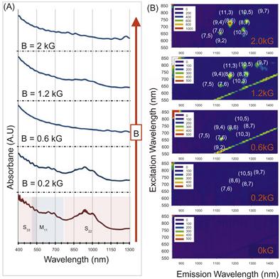
Figure 6.11 The evolution of UV–Vis–NIR (A) and PL spectra (B) of the purified samples produced at different magnetic field strengths, (0–2) kG, is shown. With increasing magnetic field strength, the diameter distribution is increasing skewed toward smaller diameter nanotubes that are visible both in the shifting of peak positions (absorbance) and in the observation of fluorescence. Source: Reprinted with permission from Ref. [181]. Copyright (2010) American Chemical Society.
The UV–Vis–NIR spectrum of the B=0 sample shows spectra typical for arc-produced SWCNTs with peaks observed in the optical absorption bands corresponding to metallic (in vicinity of 650 nm) and semiconducting (around 900 nm) SWCNTs respectively. As is typical for many synthesis methods, the B=0 sample was enriched with semiconducting tubes around the roughly 2:1 ratio expected from the combinatorial probabilities when wrapping the graphene sheet. The apparent purity by the Haddon method, revised denominator=0.141 [122], was ≈72% for this sample, indicating that the dispersed SWCNTs are well purified by the dispersion and centrifugation process steps. It should be noted that the spectrofluorometer used in this study is unable to detect SWCNTs produced by the arc without a magnetic field due to their relatively large diameter, ≈1.5 nm typical for arc method production [116], which fluoresce from their S11 transitions at wavelengths beyond the long wavelength range of the InGaAs array detector (≈1600 nm).
Now let us consider the evolution of spectra with increase of magnetic field. Firstly, the UV–Vis–NIR spectrum of the nonzero B sample demonstrates overall decrease of peak intensities corresponding to decrease of SWCNT production yield of both metallic and semiconducting nanotubes. Secondly, both UV–Vis–NIR and PL spectra indicate that increase of B-field leads to production of greater variety of semiconducting SWCNT diameters with an overall shift to smaller diameters. This is evidenced by the appearance of new peaks in the nonzero B samples with peak positions around 800 nm on UV–Vis–NIR spectra and new chiralities observed on PL spectra.
To better characterize the produced materials, an additional processing to separate enriched semiconducting and metallic fractions [123] was performed. Below results obtained using separation of semiconducting and metallic SWCNTs are described.
Three layers formed in the test tube after electronic type separation are schematically shown in Figure 6.12C and D by green (bottom layer containing mostly semiconducting SWCNTs), blue (upper layer—metallic SWCNTs), and red (medium—mixture) colors.

Figure 6.12 UV–Vis–NIR spectra of purified nonseparated samples without (A) and with (B) magnetic field. Semiconducting/metal separated samples without (C) and with (D) magnetic field. The sample without an applied magnetic field separates in a manner typical for electric arc synthesized nanotubes as previously reported in the literature [25,124]. The sample synthesized in the magnetic field separates differently due to the altered distribution of diameters; this effect is driven by both the intrinsic change in buoyancy with diameter and the altered interactions with cosurfactants by the diameter change. Source: Reprinted with permission from Ref. [181]. Copyright (2010) American Chemical Society.
UV–Vis–NIR spectra of three layers are also presented in Figure 6.12C and D (green curve from semiconducting SWCNTs layer, blue—metallic SWCNTs layer, and red—from mixture layer). It is seen in Figure 6.12C (B=0 sample) that well pronounced peaks in semiconducting and metal SWCNT bands were observed in corresponding layers of the test tube. In contrast, the UV–Vis–NIR spectrum of the nonzero B sample showed reduced peak features in the layer where the typical metallic arc was separated and was similar to that from graphenic-like structures [125]. This indicates that the population of typical arc diameter metallic SWCNTs was significantly reduced by the application of the magnetic field. The spectrum from semiconducting layer had greater variety of peaks in comparison with the B=0 sample, which correspond to production of semiconducting SWCNTs with smaller diameter.
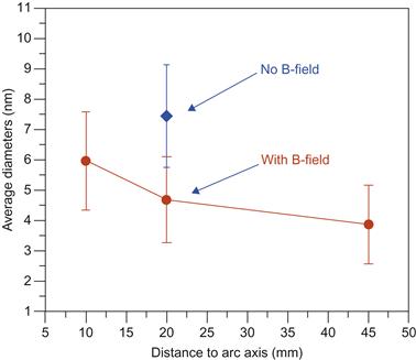
Thus both UV–visible–NIR and PL indicate that magnetically enhanced anodic arc yields broader spectrum of diameters of synthesized SWCNTs and smaller diameters compared with that without magnetic field. Such behavior is closely related to the change of catalyst particle motion in the presence of magnetic field. One possible pathway that can explain effect observed is the effect of magnetic field on catalysis particle nucleation [126]. The mechanism leading to catalyst nanoparticle diameter decrease is related to acceleration of the nickel-contained (magnetic) particles by the magnetic force toward the magnet when the temperature drops below the Curie point. In the center of the arc, the temperature is about 3000 K, while in the catalyst particle growth region the temperature is below 1800 K and can reach the Curie point toward the outer region.
Upon reaching the temperature below the Curie point, catalyst particles are accelerated toward the magnet thus reducing the residence (i.e., growth) time. As a result, catalyst particle diameter is expected to be smaller in the case of a magnetic field as compared to the case without a magnetic field as shown in Figure 6.13.
6.2.4 Synthesis of graphene in arc plasmas
With an external magnetic field applied to the discharge, the plasma temperature and density significantly increase. The plasma density strongly increases due to the effect of the magnetic-field-related focusing of the plasma jet. Indeed, magnetic confinement restricts the plasma boundaries and prevents the plasma from expansion. Another reason is the magnetization of plasma electrons which leads to more effective ionization of the neutral gas atoms by electron impact. The plasma temperature, in turn, increases in the magnetic field due to the stronger electric field in the magnetized plasma, in contrast to the nonmagnetic conditions [39,127]. Schematically, the magnetically controlled process is shown in Figure 6.14. The carbon samples were collected from the discharge enhancing/separating magnet unit (DESMU) side and top surfaces, and from the chamber walls.

Figure 6.14 Experimental setup, photo of the plasma reactor and discharge, and SEM micrographs of representative graphene flakes. (A, B) Representative SEM images of the carbon deposit collected from different collection areas. Ropes of CNTs found on the top and side surfaces of the DESMU, in the areas close to the discharge; graphene layers found on the top and side surfaces of the DESMU, in the areas remote from the discharge. An effective separation of the two different carbon nanostructures was ensured. (C) Schematic of the experimental setup. (D) Photograph of the experimental setup. (E) Schematic of the mutual position of the cube-shaped magnet, anode and cathode, and the computed 2D map of the magnetic field (field strength of 1.2 kG in the discharge gap was optimized for the highest yield of both graphene particles and CNTs). (F) Consecutive photographs of the discharge development in the nonuniform magnetic field. Source: Reprinted with permission from Ref. [70]. Copyright (2010) by Royal Society of Chemical.
In the growth zone, the ambient temperature is much higher than the Curie point of the catalyst nanoparticles which therefore remain hot and nonmagnetic. This is why the growth conditions are determined by the high catalyst temperature and also a strong incoming flux of carbon material. Outside of the optimum growth zone, the plasma temperature and hence the catalyst temperature decrease sharply. Further away, the temperature decreases below the Curie point, the catalyst particles become ferromagnetic, respond to the magnetic field, and the separation process starts. Thus, the boundary between the growth and the magnetic separation zones is determined by the catalyst alloy and the plasma parameters. Indeed, in the high-density plasma, the catalyst is hot and nonmagnetic; both graphene particles and CNT are developing in the optimum growth zone with no magnetic separation [71,128].
In the separation zone, the plasma density and the temperature are low, and the catalyst is cold. Hence, while the growth is disabled, the magnetic separation starts. To this end, the optimized composition of the two transition metals, yttrium (which is paramagnetic) and nickel (ferromagnetic with the Curie temperature of about 350°C), was used. Nickel exhibits very high carbon solubility but does not form carbon-containing compounds without oxygen, thus ensuring an efficient carbon supply to the nanostructures [129]. On the other hand, yttrium easily forms carbides and as such enables a very quick nucleation of the carbon nanostructures. Note that the melting points for both these metals are very close, so the catalyst alloy nanoparticles have a stable aggregate structure. In this way, the Y–Ni catalyst alloy was customized to exhibit the excellent nucleation/growth support ability when hot (in the optimum growth zone) and the ferromagnetic response when cooled down below 350°C (in the magnetic separation zone). Experiments have proven the effectiveness of this catalyst alloy for the large-scale carbon nanostructure production [39].
Figure 6.15 shows the images of the representative structures produced. The nanostructured carbon (nanotubes and graphene flakes) could be found on the magnet surfaces only, whereas lacey carbon was found only on the chamber walls. The carbon samples were collected and then analyzed with the SEM, TEM, atomic force microscopy (AFM), and micro Raman techniques. In Figure 6.15, we show representative SEM and TEM images of carbon samples collected from various parts of the setup. Figure 6.15A–C shows the low-, medium-, and high-magnification SEM images, respectively, of the samples containing graphene layers, collected from the top and side surfaces of the magnet (see Figure 6.15).
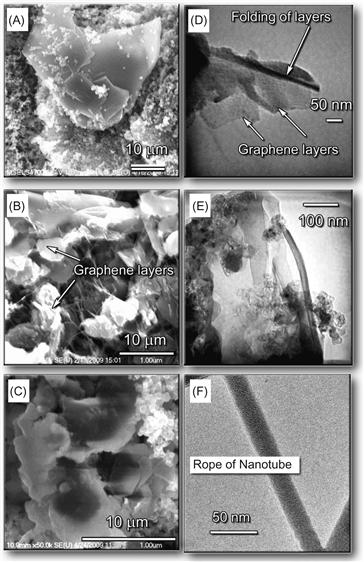
Figure 6.15 Representative SEM and TEM images of various carbon deposits collected in different collection areas. (A–C) Low-, medium-, and high-magnification SEM images of the samples containing graphene layers, collected from the top and side surfaces of the magnet. (D, E) TEM image of folded graphene layers in the carbon sample collected from the top and side surfaces of the magnet, respectively. (F) TEM image of the sample containing CNT bundles, collected from the side surfaces (remote from the discharge) of the magnet. Source: Reprinted with permission from Ref. [70]. Copyright (2010) by Royal Society of Chemical.
The estimated size of the graphene flakes is approximately 500–2500 nm, with up to 10 graphitic layers. Some graphene flakes show explicit crystallographic faceting (e.g., clearly visible hexagon sections in Figure 6.15C). It is also seen that the graphene flakes are surrounded and partially covered by loose carbon. Figure 6.15D and E shows TEM images of folded graphene layers in the carbon samples collected from the top and side surfaces of the magnet, respectively. It is seen that these fragments contain a few flake-like graphene layers, up to 3. In Figure 6.15F, it is shown the TEM image of the sample containing CNTs, collected from the side surfaces (remote from the discharge) of the DESMU. It should also be pointed out that a typical catalyst size found by the TEM was approximately 2–10 nm. The SEM analysis of the deposits found on the magnet allows a rough estimate of the production rate to be about 1 cm2 of graphene per hour of operation.
The results that characterize the samples collected at the top surface of the DESMU by the AFM, Raman, and selected area electron diffraction (SAED) techniques are shown in Figure 6.16. The AFM clearly revealed the presence of flake-like structures with the surface size of around 1 µm and a height variation of 1–5 nm (Figure 6.16A and B). The Raman characterization of the specimens collected from the side surfaces of the magnet showed the occurrence of a weak D-peak at around 1325 cm−1, which is related to the amount of defects in sp2 bonds (Figure 6.16C) [130]. The SAED TEM pattern from a similar specimen collected from the top surface of the magnet is shown in Figure 6.16E. It reveals the pattern expected for a hexagonal close-packed crystal with the incident beam close to (0001) plane.
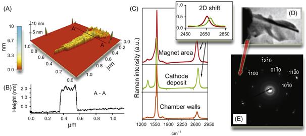
Figure 6.16 Microanalysis of the samples shown in Figures 6.1 and 6.2 (A and B). 3D reconstruction and profile of the specimens collected at the top side of the magnet. The presence of flake-like structures with the surface size of around 1 μm2 and a height variation of 1–2 nm, as well as the occurrence of “bumps/wrinkles” with the height variation of about ~0.5 nm are clearly revealed. (C) Raman spectra of the samples collected from the side surfaces of the magnet, cathode, and chamber walls. (D) Fragment of TEM photo of the folded graphene layers. (E) SAED pattern generated by the specimen collected from the top surface of the magnet. Source: Reprinted with permission from Ref. [70]. Copyright (2010) by Royal Society of Chemical.
It should be pointed out that the magnetic field strongly enhances the arc discharge. Indeed, with the DESMU installed, the plasma arc (normally confined between the cathode and the anode) is stretched toward the magnet as shown in Figure 6.17. In the video snapshots shown in Figures 6.17, it can be noted that the presence of the magnet results in deviation of arc plasma in the direction of J×B force. It was also observed that the geometry of arc plasma column did not change by removing the nickel catalyst from the anode. This means that the influence of magnetic field on nickel catalyst particles motion does not affect overall geometry of plasma column. It is possible to control distribution of magnetic field by changing the position of permanent magnet, and consequentially the growth region of carbon nanostructures can be easily manipulated according to the J×B direction. SWCNT and graphene flakes are collected in the different areas. The sample collected from the surface of Mo sheet where the arc plasmas jet was directed contains high-quality and large-scale graphene. Experimental observations suggest that the graphene is growing by a surface precipitation mechanism [131].

Figure 6.17 Distribution of magnetic field simulated by FEMM 4.2 (A), simultaneous photographs of arc plasmas jets from the front (B) and right (D) viewports, and schematic diagram (C) of electrodes position and direction magnetic field for the case when the interelectrode gap is positioned about 75 mm above the bottom of magnet.
6.2.5 Current state of the art of plasma-based synthesis of carbon nanostructures
In this section, we describe most pressing issues and current state of the art associated with synthesis of carbon nanoparticles in plasma-based synthesis technique.
6.2.5.1 Large-scale production
Large-scale and high-purity synthesis of SWNT by arc discharge stills remain very important objectives of the nanotechnology research [132–138]. Indeed, the majority of the surface-based methods, such as micromechanical exfoliation [139], epitaxial growth on electrically insulating surfaces [140] and graphene formation by thermal decomposition [141], or thermal annealing of silicon carbide [142] have not reached the expected yields [143]. Some promising results of graphene production in arc discharge [144] and separation of graphene and SWNTs were published recently, pushing further state of the art [128,144].
6.2.5.2 Control of synthesis
For a long time, arc-discharge technique was based on a trial-and-error approach and this is why ability to control and tailor the synthesis process is one of the most highly topical and pressing issues. To large extend, problem with control of the synthesis arises from the complicated nature of arc-discharge process preventing for the fixing of the elementary process of catalyst formation, carbon precipitation, and nanoparticle nucleation in space and time domain. Although the mechanism of the formation and growth of SWNTs in an arc discharge was studied for a decade, the region in arc discharge in which SWNT synthesis occurs and the temperature range favorable for SWNT growth remains unclear. According to some authors [78], the nanotube formation occurs on the periphery of an arc column at a moderate temperature range of 1200–1800 K, while other studies suggested that it is the cathode sheath adjacent to hot arc column (~5000 K) where the nanotube growth occurs [80,145,146]. Recall that in the cathode sheath region, the temperature might be well above the reported critical temperatures of thermal stability of the nanotubes. Thermal stability of SWNTs produced in helium arc was studied [94]. Using a furnace, temperature conditions (for SWNT sample) closely resembling the natural conditions of SWNT growth in the arc plasma were created. The maximum temperature determined from electrical resistance measurements combined with SWNT dynamics analysis was used for predicting SWNT synthesis region. It was concluded that SWNTs produced by an anodic arc discharge and collected in the web area outside the arc plasma are originated from the arc-discharge peripheral region, i.e., plasma–gas interface.
6.2.5.3 Outlook
In a quest for optimization of the synthesis technique and control of the SWNT diameter and chirality, the detailed comparison of SWNTs synthesized with and without magnetic field was carried out using UV–Vis–NIR and NIR fluorescence spectrometry as shown in Section 6.2.3. It is accepted that SWNTs are created by rolling up a hexagonal lattice of carbon (graphite). Rolling the lattice at different angles creates a visible twist, chirality, or spiral in the SWNT’s molecular structure, though the overall shape remains cylindrical. The SWNT’s chirality, along with its diameter, determines its electrical properties with the chiral numbers uniquely defining the SWNT diameter [147]. The armchair structure has metallic characteristics. Both zigzag and chiral structures produce band gaps, making these nanotubes semiconductors and, thus, dependent on chirality SWNT can have metallic or semiconductor conductivity. UV–Vis–NIR diagnostics demonstrated that application of the magnetic field strongly changes the outcome product with the diameter range broadens toward the smaller diameter. The data given in Table 6.1 suggest that the length, diameter, and thus chirality of arc-produced SWNTs can be controlled by external magnetic field applied to the discharge [148]. Magnetic field of relatively small magnitude of several kG was found to result in dramatically increased production of smaller diameter (about 1 nm) SWNTs and broaden of spectrum of diameters/chiralities of synthesized SWNTs.

In spite of a decade-long intense research, some basic understanding of the arc-discharge technique is still lacking and, as such, warrants detailed basic studies. Recent research advance demonstrates that CNT parameters can be controlled by a magnetic field. The summary of these results is given in Table 6.1. It is clear that SWNT parameters are coupled with properties of catalyst nanoparticle. This leads to the conclusion that the control of the arc-discharge synthesis is directly related to the fundamentals of the catalyst formation and interaction of catalyst with the active carbon species. Most critical areas where research is needed fall within the broad program of basic understanding of the arc-discharge technique by utilizing most advances experimental techniques and simulations.
Several experimental techniques under development can be utilized to probe the plasma and nanostructures in an arc. One of the possible techniques is the Langmuir probe [149]. The applicability of Langmuir probe technique for highly collisional plasma of atmospheric anodic arc producing SWNTs remains subject of active ongoing investigation. A limitation of the application of Langmuir probes in the conditions of nanostructure producing arc is caused by the very fast contamination of the probe with the synthesized nanoproducts [150]. In this respect, fast-moving probes providing exposure times to the plasma environment in the millisecond range was shown to be robust technique for plasma diagnostics [150]. Recent application of laser-induced fluorescence (LIF) and laser-induced incandescence (LII) for conditions of nanotube synthesis using laser ablation and Rayleigh microwave scattering for small-scale atmospheric plasmas opens up wide spectra of new prospects for in situ diagnostics of arc SWNT synthesis [151].
6.3 Nanoparticle synthesis in electrical arcs: modeling and diagnostics
6.3.1 Arc-discharge plasma
It was already mentioned above that the arc-discharge synthesis of carbon nanoparticles is a very promising plasma-based technique [117]. On the other hand, the controllability and flexibility of the arc-plasma-based process may be significantly improved by the use of a magnetic field (Section 6.2), which strongly influences the plasma parameters [127]. In fact, it was shown that the high-purity MWNTs can be grown in the magnetically enhanced arc discharge [38] and it was demonstrated that the use of the magnetic-field-enhanced arc discharge is very promising for the production of the long SWNTs [39].
Experimental efforts to understand the arc plasma mechanism of synthesis concerned with anode erosion mechanism [152], current–voltage characteristics of the arc discharge [153], and cathode deposit mechanism [154]. In particular, it was demonstrated that anode erosion increases with anode radius decrease, current–voltage characteristics have typical V-shape, and radius of the cathode deposit increases with arc current as shown in Figure 6.18.
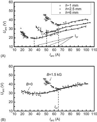
Figure 6.18 V–I characteristics of arc for different interelectrode gap sizes (h) for p=300 Torr: (A) for different gaps and B=1.5 kG and (B) comparison of two V–I characteristics with and without magnetic field for h=6 mm. Source: Reprinted with permission from Ref. [153]. Copyright (2008) by American Institute of Physics.
CNT synthesis is a relatively recent application of the anodic arc discharge and only few theoretical models related directly to this application were developed. A 1D model (in axial direction) of the SWNT formation was developed and the SWNT growth rate in the anodic arc discharge was calculated [76]. In that model, some simplified gas phase analysis was employed to calculate the nanotube growth rate. The axial velocity of the carbon outflow from the anode was estimated from the measured erosion rate and thus such model is not predictive. Moreover, the temperature of the anode was given a priori, while another work showed the anode temperature dependent on the gas pressure [79]. In all existing models, there is no coupling between the interelectrode plasma and electrode phenomena such as ablation and electron emission.
6.3.1.1 Model of the arc discharge
In order to obtain transparent solution while preserving main physical effects relevant to SWNT synthesis, we develop a global (integral) model of an anodic discharge shown schematically in Figure 6.19 [155].
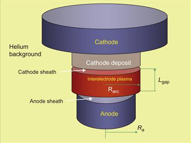
Figure 6.19 Schematics of the interelectrode gap. Source: Reprinted with permission from Ref. [155]. Copyright (2008) by American Institute of Physics.
The main features of the model are coupling between the interelectrode plasma and electrodes, current continuity at the electrodes, thermal regime of the electrodes, and the anode erosion rate. A steady-state operation of the arc discharge with carbon electrodes (anode diameter is about 6.35 mm, while the cathode diameter is about 12.5 mm) is considered. Typical interelectrode gap is in the range of about 2–5 mm. During the arcing period, carbon species are supplied by anode erosion which is determined by the anode temperature. In turn, anode temperature is affected by the heat flux from the interelectrode plasma which is controlled by pressure of the ablated species. On the other hand, the experiment indicates that erosion of the cathode is negligible during the arcing. Ablated carbon species expand and interact with background gas (helium) at atmospheric pressure condition. Dynamic boundary of the arc (the arc radius) is therefore determined by the interaction of carbon vapor with the helium background.
In order to describe the plasma state in interelectrode gap of the arc discharge, we invoke the following model formulation. We start with energy balance of the interelectrode plasma [156]:
![]() (6.6)
(6.6)
where Iarc is the arc current, Ie is the electron current at the cathode, Upl is the potential drop in the interelectrode gap, Uc is the cathode voltage, Iion is the ion current at the cathode, Te is the electron temperature, Ua is the anode voltage, Uiz is the ionization potential of carbon, Rarc is the arc radius, Lgap is the interelectrode gap length, ne is the electron density in the interelectrode gap, νe is the electron collision frequency, and Ta is the neutral temperature. In this equation, the left-hand side term is Joule heating while right-hand side terms are heat losses to the anode, losses due to ionization, and heat transfer from electrons to neutral species. It is assumed that heavy particles (ions and neutrals) are in equilibrium and have the temperature which is equal to anode temperature.
Current continuity at the cathode implies that part of the current can be conducted by electrons emitted from the cathode so that the total arc current at the cathode consists of ion and electron current:
![]() (6.7)
(6.7)
Balance of energy at the cathode is determined by heat flux from the interelectrode plasma and by the heat losses due to radiation and heat conduction [157]:
![]() (6.8)
(6.8)
where qrad and qcon are heat losses due to radiation and conduction, respectively, and φw is the work function. According to Eq. (6.8), power deposited at the cathode is dissipated by thermal conduction through the cathode and by radiation, where qcon=(Tc−T0)λ/(π3/2Rc) and ![]()
Increase of the cathode surface temperature leads to thermoionic emission. Thermoionic electron current density is determined as follows:
![]() (6.9)
(6.9)
where A is the constant dependent on cathode material and Tc is the cathode surface temperature. In the present model, the last equations (Eqs (6.7)–(6.9)) determine the solution for cathode surface temperature and cathode voltage. This can be illustrated in a more explicit manner. Firstly, by expressing cathode voltage from Eq. (6.8) and combining with Eq. (6.7), an explicit expression for the cathode voltage can be obtained in the following form:
![]() (6.10)
(6.10)
On the other hand, by combining the current continuity equation (Eq. (6.7)) with expressions for the electron and ion currents, we arrive at the following nonlinear equation for cathode temperature:
 (6.11)
It should be pointed out that the second term on the right-hand side of Eq. (6.11) is the ion current density. The ion current density is calculated based on assumption that the cathode sheath is collisionless and thus the Bohm condition at the cathode sheath edge can be used [158,159]. In addition, we want to note that electron density is the plasma parameter that couples cathode sheath model with the model of the interelectrode gap. Total arc current (used in Eq. (6.11)) is a given (known) parameter in this consideration. The interelectrode voltage, Upl, can be calculated as Upl=IarcLgap/(σπRarc2). We assume that interelectrode plasma reaches the local thermodynamic equilibrium (LTE) so that the plasma composition and ionization fraction of the gas can be calculated using Saha equation [160].
Anode sheath is established to provide current continuity at the anode. It will be shown below that anode voltage is negative under considered condition, i.e., anode sheath leads to decrease of the electron flux that reaches the cathode. Thus, anode potential drop is calculated as follows:
![]() (6.12)
(6.12)
Heating of the anode by electrons leads to anode temperature increase. Anode temperature is determined by the heat diffusion equation in the anode body:
![]() (6.13)
(6.13)
where a is the thermal diffusivity. The boundary conditions at the anode surface for this equation take into account heat conduction as well as strong erosion:
![]() (6.14)
(6.14)
where qa is the anode heat flux density, Γ is the ablation flux (kg/m2 s), T0 is the initial anode temperature, cp is the specific heat of carbon, and ΔH is the heat of vaporization of anode material (which is carbon in our case). The heat flux to the anode can be calculated as follows [161]:
![]() (6.15)
(6.15)
Anode erosion is calculated based on the Langmuir model [162]. It should be pointed out that a more accurate kinetic model may be used for ablation rate calculations (see Chapter 1). However, in our case, the arc discharge is diffuse and therefore vapor pressure near the anode is relatively small. As a result, Langmuir model predictions are close to those predicted by the kinetic model and, as such, the Langmuir model turns out to be satisfactory in this situation.
One of important characteristics of the interelectrode plasma in arc discharge is the arc radius. Being that this is an integral model of discharge that does not take into account spatial variation of plasma parameters, arc radius must be given as an input parameter.
Experimental study indicated that arc radius depends on arc current [154]. Since cathode deposit radius is determined by the radius of the arc column [154], the data shown in Figure 6.20 suggest that the arc radius varies with the arc current and can be described as follows:
![]() (6.16)
(6.16)
![]() (6.17)
(6.17)
where α=0.02 is a coefficient obtained from experiments [154]. The relations (6.16) and (6.17) were used to obtain solution of the system of equations (6.6)–(6.15).

Figure 6.20 Dependence of the cathode deposit diameter on arc current (p=500 Torr). Insert shows photographs of cathode deposit for Iarc=55 A (on left) and 75 A (on right).
The total discharge current consists of electron and ion currents. For the energy balance at the cathode, it is important to know the ion current fraction (Iion/Iarc). The dependence of (Iion/Iarc) on the discharge current is shown in Figure 6.21. On can see that (Iion/Iarc) initially decreases and then slightly increases with arc current and also increases with helium pressure.
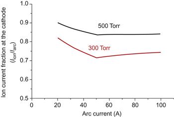
Figure 6.21 Ion current fraction at the cathode vs. arc current with gas pressure as a parameter. Source: Reprinted with permission from Ref. [155]. Copyright (2008) by American Institute of Physics.
Cathode voltage has strongly nonmonotonic dependence on the arc-discharge current as shown in Figure 6.22. Initially cathode voltage decreases with arc current increase until about 50 A, reaches the minimum, and then increases. Nonmonotonic trend is also displayed for some other arc parameters. In particular, anode sheath voltage as well as plasma voltage (potential drop in the interelectrode gap) initially increases with arc current and then decreases as shown in Figure 6.22. In addition it is shown that all voltages depend on the helium pressure. Higher helium pressure leads to higher plasma density (see below) resulting in higher ion current fraction as shown in Figure 6.21. Electron temperature and electron density initially increase with arc current as it is shown in Figures 6.23 and 6.24. This dependence can be explained by increase of the power deposition into the plasma (Joule heating) with increase of the arc current. When arc-discharge current increases above the about 50 A, arc radius increases leading to increase of the plasma volume. In turn, this leads to decrease in the electron temperature, plasma density, and ionization fraction in the interelectrode gap. According to our calculations, the interelectrode plasma is characterized by ionization degree of about 0.002–0.004.
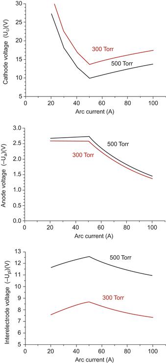
Figure 6.22 Voltages (cathode, anode, and interelectrode) dependence on the arc current with gas pressure as a parameter. Source: Reprinted with permission from Ref. [155]. Copyright (2008) by American Institute of Physics.

Figure 6.23 Electron temperature dependence on the arc current with gas pressure as a parameter. Source: Reprinted with permission from Ref. [155]. Copyright (2008) by American Institute of Physics.

Figure 6.24 Electron density dependence on the arc current with gas pressure as a parameter. Source: Reprinted with permission from Ref. [155]. Copyright (2008) by American Institute of Physics.
Similarly, cathode temperature has nonmonotonic dependence on the arc current as shown in Figure 6.25. On the other hand, anode surface temperature increases monotonically with arc current as plotted in Figure 6.25. Such dependence can be explained by monotonic increase of the power deposition into the anode with arc current increase. Monotonic increase of the anode surface temperature leads to anode ablation rate increase as displayed in Figure 6.26. Experimental data is also shown for comparison. One can see that general trend is captured by the model while the model predicts relatively moderate increase of the ablation rate in comparison with experiment.

Figure 6.25 Cathode and anode temperatures vs. the arc current with gas pressure as a parameter. Source: Reprinted with permission from Ref. [155]. Copyright (2008) by American Institute of Physics.

Figure 6.26 Anode erosion rate vs. the arc current and comparison with experimental data [153].
Calculated voltage–current (V–I) characteristic of the arc discharge is shown in Figure 6.27. One can see that calculated arc voltage (square symbols in Figure 6.27) initially decreases with arc current, reaches the minimum, and then increases. Such trend is generally in agreement with experimental data as shown in Figure 6.27 for comparison. It should be pointed out that nonmonotonic behavior of the arc voltage displayed in Figure 6.27 is the result of cathode voltage dependence on the arc current as described above and therefore is a direct consequence of model condition that arc radius increases with arc current (for I>50 A). To illustrate the effect of the assumption regarding the arc radius on the arc voltage, the calculations were performed for constant arc radius (which is equal to the anode radius). These results are plotted in Figure 6.27. It can be seen that in this case, the arc voltage decreases monotonically with arc current over the entire range of arc currents.
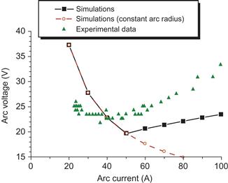
Figure 6.27 Arc voltage dependence on the arc current and comparison with experimental data [153]. The calculated arc voltage dependence on arc current based on the assumption about constant arc radius (open circle) is shown for comparison. Source: Reprinted with permission from Ref. [155]. Copyright (2008) by American Institute of Physics.
It should be pointed out that nonmonotonic dependence of arc-discharge parameters on the arc current is a direct outcome of considered condition that the arc radius changes with arc current. Thus the main issue of the present model is implementation of experimentally observed variation of arc radius with arc current which determines features of all calculated results. In fact it was concluded that nonmonotonic behavior of the arc voltage can be only reproduced by considering arc radius increase with arc current. In this model, we have assumed linear variation of the arc radius with arc current in accordance with experimental observations. As a result, calculated results display sharp nonsmooth variation of properties with the turning point at about 50 A.
Calculations show that both cathode voltage and cathode temperature exhibit nonmonotonic behavior with arc current increase. In general, in arc discharges, the cathode voltage is determined by the amount of energy deposition into the cathode required to provide electron emission. Initially arc-discharge current increase leads to higher cathode temperature resulting in higher electron emission current. As a consequence of electron current increase, the cathode voltage contributing to cathode heating decreases. When the arc current is higher than about 50 A, the arc radius increases leading to decrease in electron density. In turn, this results in ion current density decrease at the cathode. Thus, electron current increase is required to maintain the arc current. On the other hand, further increase of the arc current requires higher electron current to support the current continuity at the cathode and thus leads to increase of the cathode voltage.
This model predicts that the cathode temperature is relatively high although significantly smaller than the anode temperature as shown in Figure 6.25. However, from experiment it is known that cathode erosion is negligible [153,154]. Recall that the cathode is in direct contact with arc plasma only during the initial stage of the discharge. During the continuous arcing (after about 30 s), part of the anode material is deposited on the cathode and forms the so-called cathode deposit. This deposit material is a porous carbon structure with properties dependent on the arc parameters [154]. Thus during the continuous arcing, cathode deposit is in contact with arc plasma protecting the cathode from the erosion. This conclusion is in agreement with experimental evidence [153,154].
6.3.2 Experimental studies of the arc-discharge plasmas for nanoparticle synthesis
Plasma diagnostics is an essential tool for the in situ studies of nanostructures formation during the synthesis processes. Combining with the postsynthesis characterizations of the nanostructures, it can establish the important correlations between external arc-discharge parameters and intrinsic nanostructure properties, thus allowing ultimate control of the synthesis process.
Several experimental techniques can be utilized to investigate the plasma and nanostructures in arc discharge. We will start with description of the Langmuir probe. In addition, a nondestructive optical spectrometry technique will be described. UV–Vis emission spectra of arc in different locations under various magnetic conditions will be analyzed to provide an in situ investigation for transformation processes of evaporated carbon and catalyst species into growing carbon nanostructures. Based on the arc spectra of carbon diatomic Swan bands, vibrational temperature in arc is determined.
6.3.2.1 Langmuir probe diagnostics
The applicability of Langmuir probe technique for highly collision plasma of atmospheric anodic arc producing SWCNT remains the subject of active ongoing investigation (see Chapter 2). The complication of use of Langmuir probes in nanostructures producing arc is the very fast condensed contamination of the probe with the synthesized carbon nanostructures leading to the uncontrollable increasing of the collecting probe area and short circuit of the probe with surrounding bodies. In this respect, probe having a fast-moving shutter, providing exposure times to the plasma environment in the millisecond range, was recently shown to be the effective technique for plasma diagnostics [163].
Three modifications of single electrostatic probes were used for arc plasma studies as shown in Figure 6.28. The first two types of regular metallic probes for measurements were relatively far from the discharge (the distance to arc center r>15 mm). In this case, probe contamination with the synthesized nanostructures was relatively low, and therefore shutter was not necessary. The circular probe oriented perpendicular to radial plasma flow expanding for the gap is shown in Figure 6.28A, while another surrounding probe used large-area prolonged cylinder covering the arc axis, oriented coaxially to the axis and equipped with opening for arc video recording as shown in Figure 6.28B. The single electrostatic probe with shutter was put in vicinity of the interelectrode gap (r=8 mm). The probe was equipped with electrically controlled shutter providing exposure time to the plasma environment in milliseconds range. Fast shutter was utilized to limit the material contamination to the probe and to prevent its fast deposition by various carbon species synthesized in arc. Such deposition may lead to uncontrollable growth of collecting area and produce inadequate data. The probe consists of a copper foil collector with 3 mm width installed inside the ceramic tube which has outside diameter of 6.3 mm. The probe opening is about 5×3 mm2 as shown in Figure 6.28C. The cylindrical shutter made of molybdenum sheet was closely fit to the outside surface of the ceramic tube and was able to slide along it, so that the collector was exposed to the plasma solely during the period of time when shutter was open. Shutter was controlled using electrically driven solenoid. The collector surface containing nanostructures deposited on it during the exposition to plasma flux was analyzed using SEM. A 1 kHz voltage sweeping voltage was applied to the probes for measurements of V–I characteristics. A wide range of gas pressures were considered, while the main focus is concerned with relatively high-pressure range of several hundred Torr corresponding to the synthesis conditions of SWCNT and graphene.

Figure 6.28 Schematic diagrams of three types of electrostatic probes. Source: Reprinted with permission from Ref. [150]. Copyright (2011) by American Institute of Physics.
The V–I characteristic of circular probe obtained at residual pressure of about 0.1 Torr is shown in Figure 6.29. The V–I characteristics demonstrated the ratio of saturation currents to positively (Ip) and negatively (In) biased probe of about 100, which is in agreement with conventional collisionless probe theory predicting this ratio to be about (M/m)0.5, where M and m stand for the mass of ion and electron, respectively. In this case, the value is about 85 for helium or 140 for carbon.
Figure 6.29 V–I characteristics of single probe at 0.1 Torr. Source: Reprinted with permission from Ref. [150]. Copyright (2011) by American Institute of Physics.
The changes of Ip and In with the increase of helium pressure are presented in Figure 6.30A. Currents were measured at 50 ms after arc ignition by surrounding probe shown in Figure 6.30B. It was observed that Ip and In remained approximately constant before the gas pressure increased to 10 Torr, but after this critical pressure, both decreased with pressure significantly. In addition, it was observed that the ratio of Ip and In changed dramatically with increase of He pressure. According to Figure 6.30B, the value of Ip/In decreased from about 100 at 0.1 Torr to about 1–4 for pressures of about several hundred Torr. The similar ratios of Ip/In of about 3–5 were observed for arcs produced in argon at the pressure of several hundred Torr. This effect can be explained by the increase of measured current at the negatively biased probe above the level of ion saturation current due to secondary electron emission from the probe surface. The V–I characteristic of the probe in high helium pressure conditions is shown in Figure 6.30.

Figure 6.30 Saturation currents and their ratios as function of helium pressure. Source: Reprinted with permission from [150]. Copyright (2011) by American Institute of Physics.
It is seen that the ratio of Ip/In was about 4 suggesting significant deviation from conventional collisionless probe theory prediction as shown in Fig. 6.31.

Figure 6.31 Typical V–I characteristic of probe taken at 500 ms after arc ignition. Helium pressure is 300 Torr.
One possible pathway leading to large current in the negative bias is the collection of nanoparticles by probe [164]. In order to assess this effect, surface of the probe in negative and positive polarities was investigated.
TEM images of surface morphology of the probe surface after interaction with arc plasma and negative voltage of 80 V applied were shown in Figure 6.32. It was observed that a large amount of nanostructures containing entangled bundles of CNT, amorphous carbon, and catalyst particles were deposited on the probe surface. The probe surface immersed in arc plasma under applied voltage bias of about +80 V are displayed in Figure 6.33. One can see that the deposit of carbon nanostructures are alike regardless the polarity of the bias.


In order to explain these results, we have invoked consideration of influence of the surrounding gas pressure on probe surface. Increase of In above the ion saturation current might be due to secondary electron emission from the probe by the Auger deexcitation of long-living excited background gas atoms (He and Ar were used in this work) on the probe surface [163].
It should be emphasized that the secondary electron current in the conditions measured here may be significantly higher than ion saturation current even for relatively low secondary electron emission coefficients of about 10−3–10−4, because the excited atom density can significantly exceed the plasma density (~1015–1017 cm−3 for excited atom density compared to less than 1013 cm−3 for plasma density) [165].
Note that if the secondary electron emission dominates the ion saturation current, the shape of V–I curve for potentials is more negative than plasma potential as well as the value of In will be significantly deviated from that measured by the conventional one utilized in collisionless case. In this case, the plasma electron temperature and plasma density no longer can be precisely determined using the standard expressions using the slope of V–I curve and the ion saturation current as described in Chapter 2. In contrary, the measurements of V–I curve for potentials below the floating potential can be used for determination of the metastable He* density. Using the diffusion theory, plasma density was estimated to be about 1018 m−3 [150].
In summary it should be pointed out that the measured V–I characteristic of single Langmuir probe in high-pressure arc shows unusually low ratio of saturation current on positively biased probe to that on negatively biased, which is about 1–4. This result was explained by additional electron current with secondary electron emission from the probe due to the deexcitation of excited background gas atoms at the negatively biased probe surface.
6.3.2.2 Analysis of emission spectra from arc plasmas
The in situ investigation of the carbon and catalyst precursor species is crucial for the understanding of the nucleation process and for mastering control over the nanoparticle synthesis. Arc plasma consists of many excited states and hence arc emission spectral measurement can offer a good way to investigate the temporal evolution and dynamics of nucleation and growth processes. Furthermore, the analysis of arc emission spectra is a noninvasion approach that provides accurate measurement compared to postsynthesis methods. There are few recent reports on the optical emission spectra diagnostics of the plasma during the CNT synthesis [163,166–168]. In this section, the effect of arc parameters on the nucleation of various precursor species in synthesis of SWCNT and graphene will be described.
Carbon nanostructures synthesis was carried out in a cylindrical stainless steel chamber with 254 mm length and 152 mm diameter as described in Section 6.2. A black copolymer cylinder with 120 mm length and 50 mm diameter was amounted outside a quartz view port of the reaction chamber [166]. Two straight holes of 1 mm diameter with 10 mm interval on the surface were drilled through the cylinder to fit optical fibers of spectrometer. According to the distance between the head of optical fiber and the arc center, one can calculate the effective spot radius in arc discharge, which equals 1.2 mm in this experimental setup. The emission spectra of the arc were measured using a spectrometer (EPP2000-UVN-SR model, StellarNet Inc.), which has the optical resolution of 1 nm with 14 µm slit and the diffracted light was recorded by a 2048 pixel CCD. For the synthesis of SWCNT without magnetic field, the first spot (N1) shown in Figure 6.34B was located in the center to analyze arc spectra in highest temperature region, while the other spot (N2) with 10 mm horizontal distance to N1 corresponding to the arc edge, which is considered the growth region (see Section 6.2). In the case of a magnetically enhanced synthesis, the two spots for optical fibers were designed differently due to the jet-shaped arc plasmas. The spot marked as B1 in Figure 6.34B was in the middle of plasmas jet, for the purpose to investigate the various species delivered by plasmas jet. The spot B2 was drilled at the edge of cylinder with 10 mm distance to B1 in order to capture the arc spectra in the tail of plasmas jet near the Mo substrate for the synthesis and collection of SWCNT and graphene.
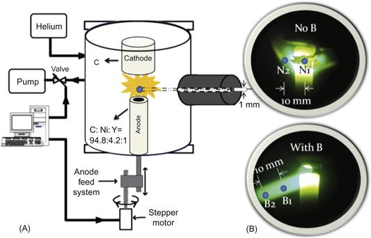
Figure 6.34 Schematic diagram of the synthesis system and spectrometer setup (A) and snapshots of arc without and with magnetic field marked with the four spots for arc emission spectra analysis (B). Source: Reprinted with permission from Ref. [168]. Copyright (2012) by American Institute of Physics.
After the arc ignition carbon, nickel, and yttrium powder are evaporated. To capture presence of various species the time-series emission spectra with interval of 190 ms were collected through the arc vapor mixture for 3 s starting from arc ignition under various magnetic fields. Figure 6.35 shows time-series emission spectra captured from spot N1 (see Figure 6.34). According to Figure 6.35, one can see that the arc emission spectra have the range from 200 to 850 nm. Main features appear at about 1.5 s after arc ignition. Typical arc emission spectra captured after 1.5 s from the arc ignition are shown in Figure 6.36. One can see that the emission spectra are dominated by carbon diatomic Swan bands (C2), which is the transition from upper electronic lever of d3Πg to lower lever of a3Πu. The prominent Swan band sequences of Δv=−2, −1, 0, 1, and 2 marked in spectra could be noticed. The emission lines of nickel (Ni I) around the wavelength of 352.5 nm and yttrium atom (Y I) at 643.5 nm are also displayed in Figure 6.36. The major peaks of spectral bands and their possible transactions during the synthesis processes are listed in Table 6.2.

Figure 6.35 Time-series emission spectra from various locations and different conditions. Source: Reprinted with permission from Ref. [168]. Copyright (2012) by American Institute of Physics.

Figure 6.36 The typical arc emission spectra in different arc spots under various magnetic conditions.
Table 6.2
The List of Identified Emission Lines from Arc Plasma and Their Possible Transitions
| Emission (nm) | Species | Transition (Band Head) |
| 352.5 | Ni I | 3d9 (2D)4s→3d9 (2D)4p |
| 361.9 | Ni I | 3d9 (2D)4s→3d9 (2D)4p |
| 438.2 | C2 | d3Πg→a3Πu (2-0) |
| 468.5 | C2 | d3Πg→a3Πu (4-3) |
| 509.7 | C2 | d3Πg→a3Πu (2-2) |
| 512.9 | C2 | d3Πg→a3Πu (1-1) |
| 516.5 | C2 | d3Πg→a3Πu (0-0) |
| 547.0 | C2 | d3Πg→a3Πu (4-5) |
| 550.2 | C2 | d3Πg→a3Πu (3-4) |
| 558.5 | C2 | d3Πg→a3Πu (1-2) |
| 563.5 | C2 | d3Πg→a3Πu (0-1) |
| 605.9 | C2 | d3Πg→a3Πu (2-4) |
| 612.2 | C2 | d3Πg→a3Πu (1-3) |
| 619.1 | C2 | d3Πg→a3Πu (0-2) |
| 643.5 | Y I |
According to the band peaks of well-defined species in arc emission spectra and assuming LTE, the Boltzmann plot method can be employed to determine the vibrational temperature [169,170].
The intensity of a spectral line transition from initial state (n) to state (m) is defined as
![]() (6.18)
(6.18)
where Nn is the density of molecules in initial state, h is Planck constant, c is speed of light, σnm is wave number emitted in the transition and Anm is the transition probability, which can be deduced as
![]() (6.19)
(6.19)
where Snm is defined as band strength between the two energy levels and gn is statistical weight of initial energy level.
The Swan bands C2 which dominate in the spectra shown in Figure 6.36 arise from transitions between the electronic states of d3Πg and a3Πu, containing well-defined vibrational heads in the Δv=−2, −1, 0, 1, and 2 sequences. Vibrational temperature can be determined according to the vibrational fine structures of C2 spectra, where the thermal equilibrium is assumed among vibrational states. Define v′ and v″ as the vibrational quantum numbers of the upper and lower vibrational levels, respectively. Hence, taking into account the two equations above, it follows that the relative emission coefficient of two vibrational lines between the d3Πg and a3Πu electronic states of the C2 molecules is given by
![]() (6.20)
(6.20)
where D is a constant and G(v′) is the vibrational energy of the upper state.
After taking logarithms, Eq. (6.20) can be deduced as
![]() (6.21)
(6.21)
According to Eq. (6.19), left-hand side term can be expressed as a function of G(v′). Therefore, the vibrational temperature is determined by the slope of the straight line obtained from the linear regression. The parameters of Swan bands C2 for temperature determination can be found in Refs [168,171]. Figure 6.37 shows the Boltzmann plots of four spots in arc under various conditions. Considering the standard errors of linear regression, the vibrational temperature of N1, N2, B1, and B2 is calculated as (6.95±1.01)×103 K, (4.19±0.60)×103 K, (5.20±0.40)×103 K, and (3.62±0.46)×103 K, respectively.

Figure 6.37 Data of Boltzmann plots calculated from the emission intensities of the C2 Swan bands for upper vibrational levels of G(v′)=0–4.
Below this measured temperature is compared with that predicted by the 2D simulations described in Section 6.3.4.
The calculated distributions of temperature and electron density in the discharge are shown in Figure 6.38. The highest numbers of temperature and density, 7020 K and 7.5×10²⁰ m−3 respectively, were observed in the arc center. The disk-like radial distribution of temperature is due to convection. The subplot in Figure 6.38 shows calculated temperature (black curve) along the radial direction from arc center and measured temperature (blue points with vertical error bar) at spots of N1 and N2 without magnetic field. Note in the context, the effective radius of spots is 1.2 mm, which is also marked as horizontal error bar shown in Figure 6.38.

Figure 6.38 The temperature and electron density distribution contours inside the discharge chamber. The subplot shows simulated temperature along the radial direction from arc center and measured temperature at spots of N1 and N2 without magnetic field. Source: Reprinted with permission from Ref. [168]. Copyright (2012) by American Institute of Physics.
Among various species detected in arc emission spectra shown in Figure 6.36, the band emission originating from C2 dominates arc spectra and it is also considered as the intermediate product of carbon vapor nucleation and the precursor of carbon nanostructures growth. The analysis of C2 band is of particular interest since it can provide an estimation of the plume temperature, which is essential to determine the growth regions of carbon nanostructures. According to the Boltzmann plots shown in Figure 6.37, the vibrational temperature of arc center (N1) without magnetic field is about 6950 K, where the mixture of carbon and catalyst powder can be evaporated to gaseous status by tremendous heat. Once the vapor mixture flows to lower temperature zone, i.e., arc plume boundary (N2), the temperature reduces to about 4000 K. The carbon atoms can nucleate with catalyst particles for carbon–catalyst alloy and then precipitate to form SWCNT. This step is considered as the essential step during the synthesis processes of SWCNT. Regarding the synthesis of SWCNT and graphene with magnetic field, the magnetically enhanced arc is confined by the Lorentz force, which generates the plasma jet (shown in Figure 6.17) and makes effective delivery of carbon particles and heat flux. The vibrational temperature in spot B1 is around 5200 K and much higher than that in spot N2. At the tail of plasma jet (B2), Mo sheet was placed on the side of permanent magnetic serving as growth substrate for graphene in terms of surface-catalyzed mechanism. The plasma jet can provide heat flux to Mo sheet continuously, keeping the vibrational temperature of spot B2 around 3600 K.
Since the density of species can be estimated from the intensity of emission, the intensity ratio of carbon and catalyst in arc emission spectra is appropriate to investigate the growth condition of carbon nanostructures. The ratio of carbon diatoms and nickel atoms in temporal evolution is displayed in Figure 6.39. The emission intensities of C2 and Ni I are selected from the wavelength of 516.5 and 352.5 nm, respectively. In the case of SWCNT synthesis without magnetic field, it can be concluded that steady-state condition is reached since the values of I(C2)/I(Ni I) in the center (N1) and boundary (N2) of arc are approximately constant. However, in the case of a magnetically enhanced arc, I(C2)/I(Ni I) in the middle of plasma jet (B1) is much larger. This is due to the fact that nickel particles (which are ferromagnetic) are attracted to the magnet and as such nickel density is depleted. Based on the TEM, Raman, and emission spectra measurements, it can be concluded that the proper density ratio of carbon diatoms and nickel atoms is around 5–7 for the synthesis of SWCNT and graphene.
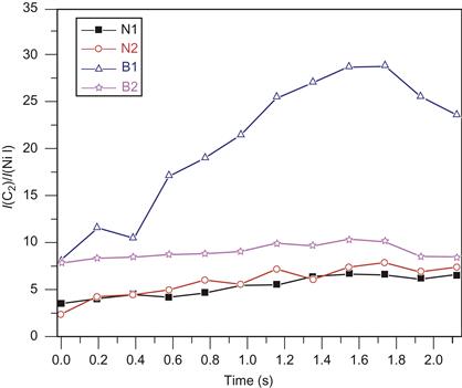
Figure 6.39 The intensity ratio of carbon diatoms (516.5 nm) and nickel atom (352.5 nm) as a function of synthesis time.
In summary, analysis of arc spectra could provide a great deal of information about the transformation and nucleation processes of different species. Simulated temperature distribution was found to be in agreement with experimental data. Based on the TEM, Raman, and emission spectra measurements, it was concluded that the proper density ratio of carbon diatoms and nickel atoms is around 5–7 for the synthesis of SWCNT and graphene.
6.3.3 Two-dimensional simulation of atmospheric arc plasmas
The purpose of the multidimensional simulation of the arc plasma is to obtain plasma parameters of the discharge relevant for CNT synthesis, which are very difficult to measure. To be useful, the numerical models should combine various phenomena such as arc operation, electrode heating, sublimation, flow expansion, species diffusion, plasma generation, and finally, nanostructure growth.
In order to obtain the temperature and species distribution, the numerical simulation of carbon arc discharge was performed [172] and will be described in this section. Electrode heating and ablation rate were coupled with flow expansion to evaluate the instantaneous mass rate of ablation self-consistently. Conservative form of Navier–Stokes equations with electromagnetic source and energy equation are solved using SIMPLER algorithm [173]. Species diffusion is solved separately for C, Ni, and Y to obtain the respective mass fractions inside the fluid domain. Ionization fractions are calculated for the individual species using Saha equation with LTE plasma assumption. Momentum and energy equations are solved using finite-volume discretization and SIMPLER algorithm to obtain velocity distribution. Power law scheme is used to obtain the fluxes on the cell faces. Energy equation is then solved to obtain the temperature distribution. Using the equation of state, overall density distribution is obtained. This order is repeated until convergence is achieved at any time step. This procedure is repeated at all time steps to obtain the transient results. Further details of modeling, boundary conditions, and the simulation are found in Ref. [172].
Axisymmetric formulation is adapted here. Formulation can be divided into five major areas: arc, sublimation, flow expansion, species transport, and ionization. The domain and boundary conditions are shown in Figure 6.40.
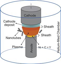
Figure 6.40 Schematics of the arc-discharge geometry and simulation domain. Source: Reprinted with permission from Ref. [172]. Copyright (2012) by American Institute of Physics.
Current continuity in electric potential form is solved to obtain the potential field and then current ![]() is obtained. Where, σ is the electrical conductivity and φ is the electric potential.
is obtained. Where, σ is the electrical conductivity and φ is the electric potential.
![]() (6.22)
(6.22)
Electrical conductivity of weakly ionized plasma in DC field is obtained using the Chapmann–Enskog equation
![]() (6.23)
(6.23)
where, e, ne, and me are unit charge, number density, and mass of electron, respectively. νe,a and νe,i are collision frequency of electron–neutrals and electron–ions, respectively, as given by:
![]() (6.24)
(6.24)
where KB, T, na, and ni are Boltzmann constant, temperature, neutrals density, and ion density, respectively. Qm is momentum transfer cross section for electrons and neutrals collision varying with temperature [161]. Coulomb logarithm, ln(Λ) of Eq. (6.25) is given in Eq. (6.26) for Ti=Te and ni=ne:
![]() (6.25)
(6.25)
![]() (6.26)
(6.26)
where ![]() and ln(γ)=0.577 [174]. The momentum transfer cross section Qm is species dependent. The collision frequencies of all the electron–neutral interactions should be added. Here the collision cross section of helium is considered for all neutrals. In general, the collision cross sections of metallic species are about two orders of magnitude greater than that of noble gases. In the present case, the evaporated material vapor density is one to two orders of magnitude less than that of He.
and ln(γ)=0.577 [174]. The momentum transfer cross section Qm is species dependent. The collision frequencies of all the electron–neutral interactions should be added. Here the collision cross section of helium is considered for all neutrals. In general, the collision cross sections of metallic species are about two orders of magnitude greater than that of noble gases. In the present case, the evaporated material vapor density is one to two orders of magnitude less than that of He.
The azimuthal component of self-induced magnetic field is obtained using Ampere’s law. Bθ is azimuthal component of magnetic field, μ0 is permittivity of vacuum, r is spatial coordinate in radial direction, jz is axial component of current flux, and R is radius of chamber.
![]() (6.27)
(6.27)
Initially, arc concentrates near the axial region and the catalyst-filled core intensively evaporates. Due to this intensive evaporation, the gap between electrodes increases near the catalyst core, and hence, the arc shifts toward the enclosed carbon shell. This transition in arc position is expected to alternate between the catalyst core and enclosed carbon shell throughout the experiment. Simulation of this transition is complicated and not necessary to obtain the overall evaporation rate. Hence, it is assumed that anode is made of single uniform compound material and arc is distributed uniformly throughout the anode tip.
Sublimation is calculated using Langmuir evaporation model (for details see Chapter 1).
![]() (6.28)
(6.28)
Γ is evaporation mass flux rate, psat is the saturation pressure, R and M are gas constant and molecular weight, respectively. Equation (6.28) is applied at all radial locations along the anode tip and plasma interface to account for the variation in surface temperature and the subsequent sublimation rate. It has to be noted here that, Langmuir model predicts higher ablation rate compared to model based on Knudsen layer kinetics (see Chapter 1) as the former does not consider the influence of background pressure on the ablation rate.
In order to find the temperature and density of fluid inside the chamber, standard Navier–Stokes equations are solved. Conservative form is used to account for the variations in density:
![]() (6.29)
(6.29)
![]() (6.30)
(6.30)
![]() (6.31)
(6.31)
where u is the velocity, μ is the viscosity, and h is the enthalpy. All the species are combined to obtain overall density and then treated as a single fluid. Velocity is zero on all solid fluid interfaces, due to no-slip, other than at the anode tip. Mass averaged velocity of the sublimated vapor at the interface is given as the boundary condition for axial velocity at the anode tip. The mass averaged velocity is obtained by dividing the evaporation mass rate with sum of vapor density and local density of fluid existing near the interface. Radial velocity and normal gradient of axial velocity are zero along the axis. Vent condition is specified on the whole bottom periphery of the chamber to maintain constant pressure inside the chamber.
Temperature on chamber walls is maintained constant at 350 K and normal gradient along the axis is considered to be zero. The chamber wall temperature 350 K is observed from the experiments. Heat flux boundary condition at the anode tip and plasma interface is given by Eqs (6.14) and (6.15).
Mass diffusion equation (Eq. (6.32)) is employed to find the distribution of individual species inside the chamber. cl and Dl are the mass fraction and diffusion coefficient of species l, respectively.
![]() (6.32)
(6.32)
Binary diffusion coefficients with hard sphere model [175] are used to account for the influence of temperature on the diffusion:
![]() (6.33)
(6.33)
where DAB is diffusion coefficient of species A diffusing into species B. MA and MB are molecular weights of species A and B. σAB is rigid sphere collision diameter.
Assuming that plasma is in LTE, Saha equation is used to obtain the ionization fractions of individual species (see Chapter 1):
![]() (6.34)
(6.34)
where, ni,l and n0,l are number density of ions and neutrals of species l, respectively. El and h are ionization energy of species l and Planck’s constant. The set of Saha equations with the ionization energies corresponding to each species is solved subjected to charge neutrality condition.
Figure 6.41 shows the direct comparison of temperature contours from the simulation (left-hand side) with the photo of experiments. Total current is 60 A and the electrodes are separated by 4 mm. In the contour plot, the temperature of plasma at the cathode periphery level is greater than 4000 K. This 1:1 comparison is not accurate in terms of plasma emission and has only qualitative character. The similarity in the shape of the temperature contour plot and photo image can be noted here.

Figure 6.41 Comparison of temperature contours (left side) with the direct image of the arc-discharge experiment with 4 mm electrode gap and total current of 60 A. Source: Reprinted with permission from Ref. [172]. Copyright (2012) by American Institute of Physics.
The current flux and self-induced magnetic field are shown in Figure 6.42A. The current flux is uniform near the anode tip and self-adjusts to a lower value toward the cathode tip. The maximum value of self-induced magnetic field is 0.0034 T. Pressure and density are shown in Figure 6.42B. Pressure of the gas inside chamber is 68,280 Pa throughout the chamber except in the arc region. Pressure along the axis near the anode tip is 68,480 Pa and decreases to 68,350 Pa in the mid arc region and then increases to 68,390 Pa toward cathode tip, due to flow stagnation. The density is low in the arc region due to high temperatures. Streamlines are shown in Figure 6.42C. The material evaporates from the anode with a velocity of 95 m/s and accelerates to 176 m/s in the mid arc region due to heat addition. The vapor then deflects away from the axis by cathode and velocity decreases gradually due to expansion. Vapor velocity is 20 m/s at a distance of 20 mm from the axis. In addition, the deflected vapor separates into two recirculation regions after hitting the chamber wall. Some of the gas leaves the chamber through the vent to maintain constant pressure.

Figure 6.42 Electromagnetic and hydrodynamic parameters in the chamber for an arc discharge with 4 mm electrode gap and total current of 60 A in 68 kPa background pressure. (A) Current flux lines with magnitude and self-induced magnetic field. (B) Mass density of the mixture (left side) and pressure (right side). (C) Streamlines with velocity magnitude. Source: Reprinted with permission from Ref. [172]. Copyright (2012) by American Institute of Physics.
Figure 6.43A and B shows the density distribution of neutral species C, Ni, Y, and their ions in the arc-discharge chamber. The highest values of density existing at the anode tip are 4.2×10²², 3.2×10²¹, and 7.8×10²⁰ m−3 for C, Ni, and Y, respectively. As expected, the quantity of carbon in the plasma exceeds that of the catalyst. The transport of species below the arc is mainly due to diffusion, whereas the diffusion and convection ensure the transport above the arc. The diffusion coefficient increases with the temperature; since the temperature in the fluid below the anode tip is high due to conduction from the anode lateral surface, the downward diffusion of species is observed in this area. Transport in radial direction is mainly due to convection. The highest densities of ions are 1.9×10²⁰, 5.5×10²⁰, and 2.6×10²⁰ m−3 respectively for C+, Ni+, and Y+. It is interesting to note that number density of C+ is lowest though it has highest neutral density. This is due to its high ionization potential. Out of the three species, Y has the lowest ionization potential and hence more Y+ are observed outside the arc, where temperatures are not sufficient to ionize C and Ni. Helium background gas has even higher ionization potential, so its ionization is negligible. Figure 6.43C illustrates the calculated distributions of temperature and electron density in the discharge with the highest numbers, 7020 K and 7.5×10²⁰ m−3 respectively, observed in the interelectrode gap. The disk-like radial distribution of temperature is due to convection.

Figure 6.43 Typical distribution of plasma parameters inside the arc-discharge chamber for Iarc=60 A, electrode gap=4 mm, and background helium pressure=68 kPa. (A) Number density of C, Ni, and Y. (B) Number density of C+, Ni+, and Y+. (C) Number density of electrons and the temperature. Note: All of the parameters coexist. Source: Reprinted with permission from Ref. [172]. Copyright (2012) by American Institute of Physics.
The flow parameter distribution for I=100 A of arc current is shown in Figure 6.44. Anode evaporation rate increases due to higher energy deposition. As a result, the species density and temperature increase inside the chamber. Figure 6.44A shows the increased spreading of neutrals in all directions. The peak density of neutrals is 6.56×10²², 5.02×10²¹, and 1.21×10²¹ m−3 for C, Ni, and Y, respectively. The peak densities of C+, Ni+, and Y+ (Figure 6.44B)) are 7.31×10²⁰, 9.89×10²⁰, and 4.25×10²⁰ m−3, respectively. A slight reduction in the thickness of the disk-like structure is noted from Figure 6.44C, which is due to the increased flow speed. However, the peak temperature in the core region is 8640 K, which is greater than that observed for I=60 A case. The peak density of electrons, for this case, is 1.6×10²¹ m−3.

Figure 6.44 Typical distribution of plasma parameters inside the arc-discharge chamber for Iarc=100 A, electrode gap=4 mm, and background helium pressure=68 kPa. (A) Number density of C, Ni, and Y. (B) Number density of C+, Ni+, and Y+. (C) Number density of electrons and the temperature. Note: Legend limits synchronized with those in Figure 6.42. Source: Reprinted with permission from Ref. [172]. Copyright (2012) by American Institute of Physics.
In the model described, an attempt was made to identify and outline the probable location of nanotube growth, directly from the simulation results. Majority of MWNTs are found in the soft core of the cathode deposit while SWNTs are found in the collaret, lateral surface of the cathode, upper wall of the chamber, and in the web suspended between cathode and chamber walls. It was also observed that, the cathode deposit has negligible amount of Ni, while it is high inside the soot deposited on the electrode lateral surfaces and in the web. The temperature distribution in Figure 6.43C also shows that temperature inside the arc region is high for Ni clusters to form. Three major theories were suggested for the growth of nanotubes: open-ended model [81], two-step growth model [84], and root-growth model [176]. Either one or all of the three mechanisms may contribute for the growth. Nevertheless, the root-growth model alone is considered here, due to the presence of large Ni clusters outside the arc region. It was shown analytically that growth of nanotubes is terminated due to the solidification of Ni clusters [177]. By considering the solidification point of 1730 K and condensation point of 3180 K, the region of nanotube growth can be outlined using the isothermal lines, directly from the simulation.
The probable growth region in vapor is shown in Figure 6.45 for I=20, 60, and 100 A. The outlined region also shows the possibility of nanotube growth on the walls of the electrodes. It can be deduced now that, the clusters grown in this region will be transported away due to convection and buoyancy, and deposited on the chamber walls. The size of growth region decreases with the increase of arc current, which is mainly due to the increases in the flow velocity as a result of increased anode evaporation rate. However, the production rate of nanoparticles does not decrease as the growth depends on the local density of contributing species which increase with the arc current as shown in Figure 6.44. Hence, there exists an optimum value of current for which production rate is the highest.
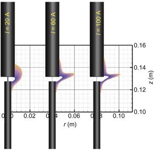
Figure 6.45 Nanoparticle growth region and number density of C and Ni for Iarc=20, 60, and 100 A. The size and configuration of growth region decreases with the increase of arc current. Source: Reprinted with permission from Ref. [178]. Copyright (2012) by Institute of Physics.
6.3.4 Model of the CNT synthesis in arc-discharge plasmas
Inside the growth region, vapor flux contributing to the growth consists of neutrals and ions of metal and carbon. The nanoparticles are negatively charged due to high mobility of electrons, creating a sheath of thickness close to Debye length, and hence ions are attracted toward the nanoparticle as shown in Figure 6.46. Nanoparticle of diameter dnp is surrounded by Debye sphere of radius dnp/2+λDe consisting of nonneutral plasma. Ions enter the sheath with Bohm speed, vB at the Debye sphere edge, and create a focused flux that contributes to the growth of nanoparticle [178]. Neutrals, on the other hand, attach to nanoparticle with thermal velocity vth. However, the focusing of ion flux vanishes if the collisions with the neutrals of background gas are dominant inside the sheath, which occurs for smaller mean free paths λmf, i.e., λDe>λmf. Besides, the nanoparticle travels at the flow speed macroscopically, which has to be considered to account for the variation in the contributing factors for nanoparticle growth [179]. The flux balance model used in Ref. [177] was for neutral vapor in the exhaust of rocket nozzles. Coming to the specific case of root-growth method of nanotubes, the effect of surface diffusion has to be considered for estimating the flux of carbon atoms. Quasi-steady form of continuum surface diffusion model was used previously for nanotube growth in stationary plasmas with constant properties [177].

Figure 6.46 Nanoparticle growth in plasma. The cluster is negatively charged. The positive ions are focused on to the cluster from Debye sheath edge with Bohm velocity. Neutrals approach the cluster with thermal velocity. Note: Not to scale. Source: Reprinted with permission from Ref. [178]. Copyright (2012) by Institute of Physics.
Let us describe the mathematical model and prediction related to the growth of CNTs in arc plasmas. The growth of catalyst clusters can be obtained by first finding the critical cluster size using Gibbs free energy of formation of a spherical cluster of radius r given by Eq. (6.35):
![]() (6.35)
(6.35)
where στ is surface energy (surface tension of isotropic materials), Va is the atomic volume, and S is the saturation ratio given by the ratio of oncoming vapor pressure pv and equilibrium pressure of the spherical cluster psat. Equation (6.35) has maxima at rc=2σVa/[kBT ln(S)] with a maximal energy of ![]() Here, rc is the radius of critical nucleate. The clusters with r≥rc are stable and grows larger with further addition of vapor atoms. Furthermore, the probable number of critical clusters may be given using Boltzmann like distribution function,
Here, rc is the radius of critical nucleate. The clusters with r≥rc are stable and grows larger with further addition of vapor atoms. Furthermore, the probable number of critical clusters may be given using Boltzmann like distribution function, ![]() as given in Ref. [180].
as given in Ref. [180].
The growth model for the cluster moving along a random path l is given by [177]:
![]() (6.36)
(6.36)
where r+ra≈r=(3/4π)1/3N1/3(2ra), N is the number of atoms in the cluster, ra is the radius of atom, r is the radius of nanoparticle, and vl is the velocity of the cluster. The coefficient β is the ratio of the vapor atoms contributing to the growth of cluster to those arriving on to the cluster’s surface. β is given as (Rarr−Revap)/Rarr. Since arrival rate (Rarr) and evaporation rate (Revap) are proportional to pressure of the vapor atoms and equilibrium pressure of the cluster, by assuming bulk vapor and cluster exist at the same temperature, Revap/Rarr=S. The equilibrium pressure psat of the spherical cluster surface can be calculated from its value corresponding to a flat surface (p*) using Kelvin’s equation, psat=p* exp[2σVa/(rRT)]. Here, r is radius of the sphere and R is gas constant. The particle flux QNi is obtained by adding neutral and ion fluxes as
 (6.37)
Finally, QNi from Eq. (6.37) is substituted in Eq. (6.35) to obtain the equation for catalyst cluster growth:
![]() (6.38)
(6.38)
where η=[1+(![]() /n)(4vB/vth)(1+(λDe/r))2]. The value of η gives the ratio of total flux to the neutral vapor flux.
/n)(4vB/vth)(1+(λDe/r))2]. The value of η gives the ratio of total flux to the neutral vapor flux.
The effective flux of carbon atoms jC directly contributing to the growth of nanotube is estimated using quasi-steady approach of continuum surface [176]:
![]() (6.39)
(6.39)
where x is the length coordinate along nanotube and QC is the rate of carbon flux from the bulk vapor arriving on the nanotube surface, Ds is the surface diffusion coefficient, and τa is the time required to absorb carbon atoms. QC, Ds, and τa are estimated using the following system of equations [176]:
![]() (6.40)
(6.40)
![]() (6.41)
(6.41)
![]() (6.42)
(6.42)
where a0 is the inter atomic distance for carbon 0.14 nm, υ is the vibrational frequency of the atoms=3×10¹³ (value based on thermal vibrations), δED is the activation energy for surface diffusion of carbon (0.3−1.8 eV), and Ea is adsorption energy (1.8−3.5 eV) [176].
Equation (6.39) is solved analytically using the following boundary conditions specified at the root (x=0) and closed end (x=L) to obtain the flux distribution:
![]()
![]() (6.43)
(6.43)
where L is the instantaneous length of nanotube, ![]() is diffusion length, and k=a0/τinc is the kinetic constant of incorporation. The incorporation time τinc can be calculated as [176]:
is diffusion length, and k=a0/τinc is the kinetic constant of incorporation. The incorporation time τinc can be calculated as [176]:
![]() (6.44)
(6.44)
Now, the increase in the length of the nanotube moving along a path l inside the chamber can be estimated using the flux balance as
![]() (6.45)
(6.45)
where Ω is area of one carbon atom in the SWCNT.
Let us now discuss some predictions by the model described. The growth region in plasma is outlined using the isotherms 3180 (inner line) and 1730 K corresponding to the condensation and solidification points of Ni. The outlined region for an arc current of 60 A is shown in Figure 6.46. Now, the path of nanoparticle in the chamber has to be traced in order to extract the vapor density and temperature local to the particle, which contributes to its growth. Since the particle size varies from nanometer to micrometer, they can be conveniently assumed to follow the streamlines of the flow. Three typical streamlines are shown in Figure 6.47. The following calculations are performed along streamline-3, which originates inside the arc core and passes through the growth region. The temperature and species distribution used for these calculations were obtained from detailed simulation of arc discharge.

Figure 6.47 Nanoparticle growth region and streamlines in the discharge chamber. Particle growth region in plasma is marked by the isotherms. The inner isotherm corresponds to 3180 K and outer isotherm corresponds to 1730 K. The streamlines 1, 2, and 3 are colored with the magnitude of velocity. Nanoparticles are assumed to follow the streamlines and growth calculations are performed along these paths within the growth region. Modeling and simulation details to obtain the streamlines and temperature distribution are found in Refs [170,176]. Source: Reprinted with permission from Ref. [178]. Copyright (2012) by Institute of Physics.
Electrode heating and sublimation rate were coupled with flow expansion to evaluate the instantaneous mass rate of ablation self-consistently. 2D electric field was considered to simulate the arc. Conservative form of Navier–Stokes equations with electromagnetic source and energy equation were solved. Species diffusion was solved separately for C, Ni, and Y to obtain the respective mass fractions inside the fluid domain. Ionization fractions were calculated for the individual species using Saha equation with LTE plasma assumption. Further details of modeling, boundary conditions, and the simulation are found in Refs [170,176]. For 60 A of arc current, the evaporation model has predicted almost double that of experiment value. Nevertheless, the trend shown the simulation for 10–100 A arc currents was consistent with the experiment values.
Growth calculations performed for I=60 A and 4 mm interelectrode gap with a background pressure of 68 kPa are shown in Figure 6.48. Mass fractions of C, Ni, and Y in the anode are 0.66, 0.25, and 0.09, respectively. Calculations are performed along streamline-3 shown in Figure 6.47. The mean free path, λmf is calculated based on neutral gas density. Here, He neutrals alone are considered as their density is more than three orders of magnitude compared to Ni. Figure 6.48A shows the effect of plasma on the growth of Ni cluster. The abscissa represents the distance along the streamline-3 starting from the isotherm corresponding to 3180 K and ending at the isotherm corresponding to 1730 K. The coefficient η shown on the left ordinate reflects the ratio of ion flux to neutral flux (η−1) contributing to the growth.
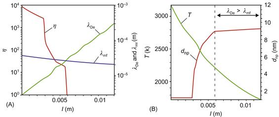
Figure 6.48 Catalyst cluster growth calculations for I=60 A. (A) Effect of plasma on catalyst nanoparticle growth and (B) diameter of the catalyst (Ni) nanoparticle. It is assumed that the ion flux contribution for the growth ceases completely for Debye length greater than mean free path of vapor. Source: Reprinted with permission from Ref. [178]. Copyright (2012) by Institute of Physics.
The ion density decreases as the particle moves away from the arc and hence η also decreases. Debye sheath thickness, λDe shown on right ordinate, increases with the reduction in plasma density. The mean free path λmf decreases due to reduction in the temperature. At l=6 mm, the ion flux to the Ni cluster ceases completely as λDe>λmf. The resultant growth is shown in Figure 6.48B. Though the flux is high in the region up to l=3 mm, cluster growth is negligibly small due to high rate of evaporation, Revap. From l=3 to 6 mm, steep increase in the particle diameter dnp is observed due to the dominance of ion flux and beyond this point, the growth rate is low due to the cessation of ion flux. The final size of the Ni cluster is around 9.3 nm. It has to be noted here that, SWCNT starts growing on the Ni cluster simultaneously, which will reduce the Ni vapor flux to the cluster. The maximum reduction in the area may be 50%. It remains relatively unknown, exactly when the nanotube starts growing on the Ni cluster. Hence, on an average, only 75% of the cluster area is considered to receive Ni vapor flux.
Arc-discharge experiment with 60 A current was carried out to measure the Ni particle size. The details are found in Ref. [126]. The diameter distribution of Ni particles in a sample taken at a distance of 20 mm from the arc axis is shown in Figure 6.49. Diameter varies from 2 to 12 nm and the highest number of particles is of 6 nm. The average size of the particles is 7.5 nm. The size of the Ni cluster obtained from the present simulation at this location is 9.2 nm. As mentioned earlier, the rate of evaporation predicted by the simulation was higher compared to experiment. The accurate values of evaporation rate may decrease the Ni concentration in the growth region leading to a reduction in the particle size. But, the flow speed also decreases simultaneously, due to low evaporation rate. The slower flow causes the particle to stay for a longer time in the growth region and eventually increases the particle size.

Figure 6.49 Diameter distribution of Ni particles measured at a distance of 20 mm from the electrode axis. Arc current was 60 A. Source: Reprinted with permission from Ref. [178]. Copyright (2012) by Institute of Physics.
Figure 6.50A shows that the ratio of total (ions + neutrals) flux to the neutral vapor flux is about 1 throughout the growth region. This means the ion flux no longer contributes to the growth of nanotube, which is evident from Figure 6.50B.

Figure 6.50 SWCNT growth calculations for I=60 A. (A) Effect of plasma on SWCNT growth. (B) Density of carbon neutrals and ions. (C) Length of SWCNT. Source: Reprinted with permission from Ref. [178]. Copyright (2012) by Institute of Physics.
The ratio of ion density to neutrals density of carbon is negligibly small (less than 10−11) even when the Debye sheath increases the collecting area. The reason for low ion flux is high ionization potential of carbon. Figure 6.50C shows the length of SWCNT as it travels along the streamline in the temperature range 3180–1730 K. The nanotube grows up to 3.6 μm long mostly due to neutrals flux.
The nanotube growth model, used here, cannot specify the diameter; however, the Ni cluster growth model can be used to specify the range of diameters. In fact it was shown that nanotubes grow as bundles as well on a single catalyst particle [21].
The SWCNT length distribution from the experiments conducted with 70–80 A arc current is shown in Figure 6.51. More details are found in Ref. [39]. The length distribution shows that 50% of the nanotubes are under 0.6 μm length while 90% are less than 1.3 μm. Also, the SEM image from Ref. [39] shows the nanotube grown up to 3.04 μm long. The growth calculations performed for 70 A and 80 A arc current are shown in Figure 6.52. The SWCNT length is 2.2 μm and 2.02 μm respectively for the arc currents 70 A (Figure 6.52A)) and 80 A (Figure 6.52B). The length obtained using the growth model agreed well with experimental data.
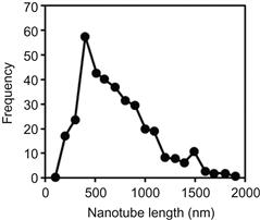
Figure 6.51 CNT length distribution from experiments with 70–80 A arc current. Further details of the experiment are found in Ref. [39]. Source: Reprinted with permission from Ref. [178]. Copyright (2012) by Institute of Physics.

Figure 6.52 SWCNT growth calculations for (A) I=70 A and (B) I=80 A arc current. Source: Reprinted with permission from Ref. [178]. Copyright (2012) by Institute of Physics.
It should be pointed out that the growth of nanoparticles can be improved by (1) increasing the size of growth region, (2) increasing the density of contributing species (Ni, Ni+, C, and C+), and (3) decreasing the velocity of nanoparticle (≈fluid velocity). For a given configuration, contributing species density and velocity are interdependent as velocity is directly proportional to the evaporation rate. Though ion flux has a significant effect on the growth rate, density of C+ may not increase without increasing the temperature above 4500 K, at which nanotubes cannot grow [176].
Keeping this in view, parametric studies were carried out by varying the arc current, background pressure, and interelectrode gap. The results are listed in Table 6.3. Columns 2, 3, and 4 represent arc current, interelectrode gap, and background pressure, respectively. The length of path traversed by nanoparticle in the growth region, l, is shown in column 5. The size of Ni cluster, dnp, and length of SWCNT, L, are given in columns 6 and 7, respectively.

The nanoparticle sizes, dnp and L, decrease with the increase of arc current. This is mainly due to the increase in the flow velocity along the growth region. The velocity increases by 40 m/s compared to case-0. Though the density of species Ni, Ni+, C, and C+ is high due to the increased evaporation, the particles quickly move out of the growth region. On the other hand, reduction in arc current has the exactly opposite effect on the growth of nanoparticles. Reduced background pressure (case-3) and interelectrode gap (case-5) accelerate the flow and decrease the species density as well. Hence the particle sizes also decrease. Increase in background pressure and electrode gap decelerates the flow and also results in the increase of species density along the streamline. The diameter of Ni cluster increases by 1.1 and 2.5 nm, and the length of SWCNT increases by 1.5 and 3.4 μm respectively for the cases 4 and 6 in comparison to case-0. The increment of pressure and interelectrode gap has limitations in terms of transformation to MWCNT growth mode and arc stability. High pressure causes the arrival rate of vapor atoms to exceed the incorporation rate, which may result in the formation of MWCNTs.
Homework problems
1. Calculate charge evolution of a 10 µm long carbon nanotube. Consider 1.5 nm diameter nanotube in carbon plasma electron density of about 1017 m−3 and electron temperature of about 1 eV. Consider collisionless sheath around nanotube and neglect electron emission from the nanotube.
2. Compute SWCNT residence time in the 2 mm plasma region having density of about 1018 m−3 and flow velocity of about 103 m/s. Consider electric field of about 1 V/m. Use conditions from problem #1 to calculate SWCNT charge in steady state.
3. Taking into account results presented in Section 6.3.2 compute the heat flux to anode and cathode in the case of 100 A arc discharge. Consider pressure of about 300 Torr, the anode diameter of about 6.35 mm, and the cathode diameter of about 12.5 mm. Both cathode and anode are made out of carbon.
4. Compute the conductivity of the weakly ionized 1 eV carbon plasma as a function of pressure. Consider that ionization degree is about 0.001.
5. Calculate the binary diffusion coefficient of carbon into helium as a function of temperature (1000–3000 K) for 1 atm arc.
References
1. Feynman R. In: Chodos Alan, ed. American Physics Society. Feynman’s Classic CalTech Lecture 1959.
2. Levchenko I, Ostrikov K, Keidar M, Xu S. Deterministic nanoassembly: neutral or plasma route? Appl Phys Lett. 2006;89:033109.
3. Ostrikov K. Plasma Nanoscience Wiley-VCH 2008.
4. Iijima S. Helical microtubules of graphitic carbon. Nature. 1991;354:56–58.
5. Novoselov KS, Geim AK, Morozov SV, et al. Electric field effect in atomically thin carbon films. Science. 2004;306(5696):666–669.
6. Dresselhaus MS, et al. Physics of carbon nanotubes. Carbon. 1995;33(7):883–891.
7. Baxendale M. The physics and applications of carbon nanotubes. J Mater Sci Mater Electron. 2003;14(10-12):657–659.
8. Lee C, Wei XD, Kysar JW, Hone J. Measurement of the elastic properties and intrinsic strength of monolayer graphene. Science. 2008;321(5887):385–388.
9. Hong S, Myung S. Nanotube electronics—a flexible approach to mobility. Nat Nanotechnol. 2007;2(4):207–208.
10. Geim AK, Novoselov KS. The rise of graphene. Nat Mater. 2007;6(3):183–191.
11. Chen SS, Wu QZ, Mishra C, et al. Thermal conductivity of isotopically modified graphene. Nat Mater. 2012;11(3):203–207.
12. Lee SB, Teh AS, Teo KBK, et al. Fabrication of carbon nanotube lateral field emitters. Nanotechnology. 2003;14:192–195.
13. Buldum A, Lu JP. Electron field emission properties of closed carbon nanotubes. Phys Rev Lett. 2003;91:236801/1–236801/4.
14. Chhowalla M, Teo KBK, Ducati C, et al. Growth process conditions of vertically aligned carbon nanotubes using plasma enhanced chemical vapor deposition. J Appl Phys. 2001;90:5308–5317.
15. Gao H, Wu XB, Li JiT, et al. Hydrogen adsorption of open-tipped insufficiently graphitized multiwalled carbon nanotubes. Appl Phys Lett. 2003;83:3389–3391.
16. Kong J, Franklin NR, Zhou C, et al. Nanotube molecular wires as chemical sensors. Science. 2000;287:622–625.
17. Schadler L, Giannaris S, Ajayan P. Load transfer in carbon nanotube epoxy composites. Appl Phys Lett. 1998;73:3842–3844.
18. Tersoff T. Energies of fullerenes. Phys Rev B. 1992;46:15546–15549.
19. Huang Z, Xu J, Ren Z, Wang J, Siegal M, Provencio P. Growth of highly oriented carbon nanotubes by plasma-enhanced hot filament chemical vapor deposition. Appl Phys Lett. 1998;73:3845.
20. Wang YH, Kim MJ, Shan HW, et al. Continued Growth of Single-Walled Carbon Nanotubes. Nano Lett. 2005;5:997.
21. Journet C, Maser WK, Bernier P, et al. Large-scale production of single-walled carbon nanotubes by the electric-arc technique. Nature. 1997;388:756–758.
22. Moravsky AP, Wexler EM, Loufty RO. In: Meyyappan M, ed. Carbon Nanotubes: Science and Applications. Boca Raton, FL: CRC Press; 2004.
23. Takikawa H, Yatsuki M, Sakakibara T, Itoh S. Carbon nanotubes in cathodic vacuum arc discharge. J Phys D Appl Phys. 2000;33:826–830.
24. Meyyappan M, ed. CarbonNanotubes: Science and Applications. Boca Raton, FL: CRC Press; 2004.
25. Farhat S, De La Chapelle ML, Loiseau A, et al. Diameter control of single-walled carbon nanotubes using argon–helium mixture gases. J Chem Phys. 2001;115:6752–6759.
26. Waldorff EI, Waas AM, Friedmann PP, Keidar M. Characterization of carbon nanotubes produced by arc discharge: effect of the background pressure. J Appl Phys. 2004;95:2749–2754.
27. Wildoer JWG, Venema LC, Rinzler AG, Smalley RE, Dekker C. Electronic structure of atomically resolved carbon nanotubes. Nature. 1998;391:59–62.
28. Bower C, Zhou O, Zhu W, Werder DJ, Jin S. Nucleation and growth of carbon nanotubes by microwave plasma chemical vapor deposition. Appl Phys Lett. 2000;77:2767–2769.
29. Kunstmann J, Quandt A, Boustani I. An approach to control the radius and the chirality of nanotubes. Nanotechnology. 2007;18:155703/1–155703/3.
30. Ando YY, Zhao X, Hirahara K, Suenaga K, Bandow S, Iijima S. Mass production of single-wall carbon nanotubes by the arc plasma jet method. Chem Phys Lett. 2000;323:580–585.
31. Zhao T, Liu Y. Large scale and high purity synthesis of single-walled carbon nanotubes by arc discharge at controlled temperatures. Carbon. 2004;42:2765–2768.
32. Lv X, Du F, Ma Y, Wu Q, Chen Y. Synthesis of high quality single-walled carbon nanotubes at large scale by electric arc using metal compounds. Carbon. 2005;43:2020–2022.
33. Tang D, Sun L, Zhou J, Zhou W, Xie S. Two possible emission mechanisms involved in the arc discharge method of carbon nanotube preparation. Carbon. 2005;43:2812–2816.
34. Yao M, Liu B, Zou Y, et al. Synthesis of single-wall carbon nanotubes and long nanotube ribbons with Ho/Ni as catalyst by arc discharge. Carbon. 2005;43:2894–2901.
35. Y. Okawa, S. Kitamura, Y. Iseki, An experimental study on carbon nanotube cathodes for electrodynamic tether propulsion, in: Proc. Ninth Spacecraft Charging Technology Conference, Japan, 2005.
36. Stepanek I, Maurin G, Bernier P, et al. Nano-mechanical cutting and opening of single wall carbon nanotubes. Chem Phys Lett. 2000;331:125–131.
37. Kostov KG, Barroso JJ. Numerical simulation of magnetic-field-enhanced plasma immersion ion implantation in cylindrical geometry. IEEE Trans Plasma Sci. 2006;34:1127–1135.
38. Anazawa K, Shimotani K, Manabe C, Watanabe H, Shimizu M. High-purity carbon nanotubes synthesis method by an arc discharging in magnetic field. Appl Phys Lett. 2002;81:739–741.
39. Keidar M, Levchenko I, Arbel T, Alexander M, Waas AM, Ostrikov K. Increasing the length of single-wall carbon nanotubes in a magnetically enhanced arc discharge. Appl Phys Lett. 2008;92:043129/1–043129/3.
40. Zheng LX, O’Connell MJ, Doorn SK, et al. Ultralong single-wall carbon nanotubes. Nat Mater. 2004;3:673–676.
41. Wang ZL, Tang DW, Li XB, et al. Length-dependent thermal conductivity of an individual single-wall carbon nanotube. Appl Phys Lett. 2007;91:123119/1–123119/3.
42. Novoselov KS, Geim AK, Morozov SV, et al. Electric field effect in atomically thin carbon films. Science. 2004;306:666.
43. Kim S, Nah J, Jo I, et al. Realization of a high mobility dual-gated graphene field-effect transistor with Al2O3 dielectric. Appl Phys Lett. 2009;94:062107.
44. Levendorf MP, Ruiz-Vargas CS, Garg S, Park J. Transfer-free batch fabrication of single layer graphene transistors. Nano Lett. 2009;9:4479.
45. Li X, Cai W, An J, et al. Large-area synthesis of high-quality and uniform graphene films on copper foils. Science. 2009;324:1312.
46. Service RF. Carbon sheets an atom thick give rise to graphene dreams. Science. 2009;324:875.
47. Chen JH, Ishigami M, Jang C, Hines DR, Fuhrer MS, Williams ED. Printed graphene circuits. Adv Mater. 2007;19:3623.
48. Geim AK. Graphene: status and prospects. Science. 2009;324:1530.
49. Lin Y-M, Jenkins KA, Valdes-Garcia A, Small JP, Farmer DB, Avouris P. Operation of graphene transistors at gigahertz frequencies. Nano Lett. 2009;9:422.
50. Kim DH, Ahn JH, Choi WM, et al. Stretchable and foldable silicon integrated circuits. Science. 2008;320:507.
51. Sekitani T, Noguchi Y, Hata K, Fukushima T, Aida T, Someya T. A rubberlike stretchable active matrix using elastic conductors. Science. 2008;321:1468.
52. Kim KS, Zhao Y, Jang H, et al. Large-scale pattern growth of graphene films for stretchable transparent electrodes. Nature. 2009;457:706.
53. Eda G, Fanchini G, Chhowalla M. Large-area ultrathin films of reduced graphene oxide as a transparent and flexible electronic material. Nat Nanotechnol. 2008;3:270.
54. Novselov KS, Geim AK, Morozov SV, et al. Two-dimensional gas of massless Dirac fermions in graphene. Nature. 2005;438:197.
55. Novoselov KS, Jiang D, Schedin F, et al. Two-dimensional atomic crystals. Proc Natl Acad Sci U.S.A. 2005;102:10451.
56. http://www.nobelprize.org/nobel_prizes/physics/laureates/2010/.
57. Berger C, Song Z, Li X, et al. Electronic confinement and coherence in patterned. Science. 2006;312:1191.
58. Ohta T, El Gabaly F, Bostwick A, et al. Morphology of graphene thin film growth on SiC(0001). New J Phys. 2008;10:023034.
59. Obraztsov AN. Making graphene on a large scale. Nat Nanotech. 2009;4:212.
60. Park S, Ruoff RS. Chemical methods for the production of graphenes. Nat Nanotech. 2009;4:217.
61. Rut’kov EV, Tontegode AY. A study of the carbon adlayer on iridium. Surf Sci. 1985;161:373.
62. Berger C, Song Z, Li T, et al. Ultrathin epitaxial graphite: 2D electron gas properties and a route toward graphene-based nanoelectronics. J Phys Chem B. 2004;108:19912.
63. http://www.darpa.mil/Our_Work/MTO/Programs/Carbon_Electronics_for_RF_Applications_(CERA).aspx.
64. Wood JD, Schmucker SW, Lyons AS, Pop E, Lyding JW. Effects of polycrystalline Cu substrate on graphene growth by chemical vapor deposition. Nano Lett. 2011;11:4547.
65. Luo Z, Lu Y, Singer DW, et al. Effect of substrate roughness and feedstock concentration on growth of wafer-scale graphene at atmospheric pressure. Chem Mater. 2011;23:1441.
66. Reina A, Jia X, Ho J, et al. Large area, few-layer graphene films on arbitrary substrates by chemical vapor deposition. Nano Lett. 2009;9:30.
67. Bunshah RF. Handbook of Deposition Technologies for Films and Coatings: Science, Technology and Applications Park Ridge, NJ: Noyes Publications; 1994.
68. Bunshah RF. Handbook of Hard Coatings: Deposition Technologies, Properties and Applications Park Ridge, NJ: Noyes Publications; 2001.
69. Qi JL, Zheng WT, Zheng XH, Wang X, Tian HW. Relatively low temperature synthesis of graphene by radio frequency plasma enhanced chemical vapor deposition. Appl Surf Sci. 2011;257:6531.
70. Volotskova O, Levchenko I, Shashurin A, Raitses Y, Ostrikov K, Keidar M. Single-step synthesis and magnetic separation of graphene and carbon nanotubes in arc discharge plasmas. Nanoscale. 2010;2(10):2281–2285.
71. Terasawa T, Saiki K. Growth of graphene on Cu by plasma enhanced chemical vapor deposition. Carbon. 2012;50:869.
72. McKelliget JW, Szekely J. A mathematical model of the cathode region of a high intensity carbon arc. J Phys D Appl Phys. 1983;16:1007.
73. Beilis II. Application of vacuum arc cathode spot model to graphite cathode. IEEE Trans Plasma Sci. 1999;27:821.
74. Lefort A, Parizet MJ, El-Fassi SE, Abbaoui M. Erosion of graphite electrodes. J Phys D Appl Phys. 1993;26:1239.
75. Bilodeau JF, Pousse J, Gleizes A. A mathematical-model of the carbon-arc reactor for fullerene synthesis. Plasma Chem Plasma Proc. 1998;18:285.
76. Hinkov I, Farhat S, Scott CD. Influence of the gas pressure on single-wall carbon nanotube formation. Carbon. 2005;43:2453.
77. Hinkov I, Grand J, de la Chapelle ML, et al. Effect of temperature on carbon nanotube diameter and bundle arrangement: Microscopic and macroscopic analysis. J Appl Phys. 2004;95:2029.
78. Farhat S, Scott CD. Review of the arc process modeling for fullerene and nanotube production. J Nanosci Nanotechnol. 2006;6:1189.
79. Keidar M, Waas AM. On the conditions of carbon nanotube growth in the arc discharge. Nanotechnology. 2004;15:1571.
80. Gamaly EG, Ebbesen TW. Mechanism of carbon nanotube formation in the arc discharge. Phys Rev B. 1995;52:2083.
81. Iijima S, Ajayan PM, Ichihashi T. Growth model for carbon nanotubes. Phys Rev Lett. 1992;69:3100.
82. Saito Y, Yoshikawa T, Inagaki M. Growth and structure of graphitic tubules and polyhedral particles in arc-discharge. Chem Phys Lett. 1993;204:277.
83. Colbert DT, Smalley RE. Electric effects in nanotube growth. Carbon. 1995;33:921.
84. Zhou D, Chow L. Complex structure of carbon nanotubes and their implications for formation mechanism. J Appl Phys. 2003;93:9972.
85. Ajayan PM, Ebbesen TW, Ichihashi T, Iijima S, Tanigaki K, Hiura H. Opening carbon nanotubes with oxygen and implications for filling. Nature. 1993;362:522–525.
86. Wagner RS, Ellis WC. Vapor–liquid–solid mechanism of single crystal growth. Appl Phys Lett. 1964;5:89–90.
87. Ding F, Rosen A, Bolton K. The role of the catalytic particle temperature gradient for SWNT growth from small particles. Chem Phys Lett. 2004;393(4-6):309–313.
88. Keidar M, Levchenko I, Arbel T, Alexander M, Waas AM, Ostrikov KK. Magnetic-field-enhanced synthesis of single-wall carbon nanotubes in arc discharge. J Appl Phys. 2008;103(9):094318.
89. Chiang WH, Sankaran RM. Linking catalyst composition to chirality distributions of as-grown single-walled carbon nanotubes by tuning NixFe1−x nanoparticles. Nat Mater. 2009;8(11):882–886.
90. Waldorff EI, Waas AM, Friedmann PP, Keidar M. Characterization of carbon nanotubes produced by arc discharge: effect of the background pressure. J Appl Phys. 2004;95:2749.
91. Keidar M, Raitses Y, Knapp A, Waas AM. Current-driven ignition of single-wall carbon nanotubes. Carbon. 2006;44:1022.
92. Ostrogorsky AG, Marin C. Heat transfer during production of carbon nanotubes by the electric-arc process. Heat Mass Transfer. 2006;42:470–477.
93. M. Kundrapu, Modeling and Simulation of Ablation-Controlled Plasmas, Ph.D Dissertation, George Washington University, 2011.
94. Volotskova O, Shashurin A, Keidar M, Raitses Y, Demidov V, Adams S. Ignition and temperature behavior of a single-wall carbon nanotube sample. Nanotechnology. 2010;21.
95. Mieno T, Takeguchi M. Thermal motion of carbon clusters and production of carbon nanotubes by gravity-free arc discharge. J Appl Phys. 2006;99:104301.
96. Winske D, Jones ME. Effect of finite charging time on particulates in RF discharges. IEEE Trans Plasma Sci. 1995;23:188.
97. Keidar M, Beilis I, Boxman RL, Goldsmith S. Non-stationary macroparticle charging in an arc plasma jet. IEEE Trans Plasma Sci. 1995;23:902.
98. Keidar M, Waas AM, Raitses Y, Waldorff E. Modeling of anodic arc discharge and condition for single wall nanotubes growth. J Nanosci Nanotechnol. 2006;6:1309.
99. Levchenko I, Ostrikov K, Tam E. Uniformity of postprocessing of dense nanotube arrays by neutral and ion fluxes. Appl Phys Lett. 2006;89:223108.
100. Lieberman MA, Lichtenberg AJ. Principles of Plasma Discharges and Materials Processing New York, NY: Wiley; 1994.
101. Keidar M, Monteiro OR, Anders A, Boyd ID. Magnetic field effect on the sheath thickness in plasma immersion ion implantation. Appl Phys Lett. 2002;81:1183.
102. Levchenko I, Ostrikov K. Nanostructures of various dimensionalities from plasma and neutral fluxes. J Phys D. 2007;40:2308.
103. Levchenko I, Rider AE, Ostrikov K. Control of core-shell structure and elemental composition of binary quantum dots. Appl Phys Lett. 2007;90:193110.
104. Gavillet J, Thibault J, Stephan O, et al. Nucleation and growth of single-walled nanotubes: the role of metallic catalysts. J Nanosci Nanotech. 2004;4:346.
105. Sen R, Suzuki S, Kataura H, Achiba Y. Growth of single-walled carbon nanotubes from the condensed phase. Chem Phys Lett. 2001;349:383.
106. Levchenko I, Baranov O. Simulation of island behavior in discontinuous film growth. Vacuum. 2003;72:205.
107. Levchenko I, Ostrikov K, Long JD, Xu S. Plasma-assisted self-sharpening of platelet-structured single-crystalline carbon nanocones. Appl Phys Lett. 2007;91:113115.
108. Baughman RH, Zakhidov AA, De Heer WA. Carbon nanotubes—the route toward applications. Science. 2002;297:2.
109. Ostrikov K. Colloquium: reactive plasmas as a versatile nanofabrication tool. Rev Mod Phys. 2005;77:489.
110. Han Z, Tay B, Tan C, Shakerzadeh M, Ostrikov K. Electrowetting control of cassie-to-wenzel transitions in superhydrophobic carbon nanotube-based nanocomposites. ACS Nano. 2009;3(10):3031–3036.
111. Li N, Wang X, Ren F, Haller GL, Pfefferle LD. Diameter tuning of single-walled carbon nanotubes with reaction temperature using a Co monometallic catalyst. J Phys Chem C. 2009;113:10070–10078.
112. Journet C, Maser WK, Bernier P, et al. Large-scale production of single-walled carbon nanotubes by the electric-arc technique. Nature. 1997;388:756.
113. Moravsky AP, Wexler EM, Loufty RO. Growth of carbon nanotubes by arc discharge and laser ablation. In: Meyyappan M, ed. Carbon Nanotubes: Science and Applications. Boca Raton, FL: CRC; 2004;65–97.
114. Stepanek I, Maurin G, Bernier P, et al. Nano-mechanical cutting and opening of single wall carbon nanotubes. Chem Phys Lett. 2000;331:125.
115. Łabedz O, Langea H, Huczko A, Borysiuk J, Szybowicz M, Bystrzejewski M. Influence of carbon structure of the anode on the synthesis of single-walled carbon nanotubes in a carbon arc plasma. Carbon. 2009;47:2847–2854.
116. Waldorff E, Waas AM, Friedmann PP, Keidar M. Characterization of carbon nanotubes produced by arc discharge: effect of the background pressure. J Appl Phys. 2004;95(5):2749.
117. Keidar M. Factors affecting synthesis of single-wall carbon nanotubes in arc discharge. J Phys D Appl Phys. 2007;40:2388–2393.
118. Karmakar S, Kulkarni NV, Nawale AB, Lalla NP, Mishra R, Sathe VG. A novel approach towards selective bulk synthesis of few-layer graphenes in an electric arc. J Phys D Appl Phys. 2009;42:115201.
119. Mohiuddin TMG, Lombardo A, Nair RR, et al. Uniaxial strain in graphene by Raman Spectroscopy: G peak splitting, Gruneisen parameters and sample orientation. Phys Rev B. 2009;79:205433.
120. Dresselhaus MS, Dresselhaus G, Eklund PC. C60-related tubilus and spherulus. Science of Fullerence and Carbon Nanotubes San Diego, CA: Academic Press; 1996; pp. 756–864.
121. Gao B, Zhang Y, Zhang J, Kong J, Liu Z. Systematic comparison of the Raman spectra of metallic and semiconducting SWNTs. J Phys Chem C. 2008;112:8319–8323.
122. Itkis ME, Perea DE, Niyogi S, et al. Purity evaluation of as-prepared single-walled carbon nanotube soot by use of solution-phase near-IR spectroscopy. Nano Lett. 2003;3(3):309.
123. Arnold MS, Green AA, Hulvat JF, Stupp SI, Hersam MC. Sorting carbon nanotubes by electronic structure using density differentiation. Nat Nanotech. 2006;1:60–65.
124. Fagan JA, Landi B, Simpson J, et al. Comparative measures of single-wall carbon nanotube dispersion. J Phys Chem B. 2006;110:801.
125. Kosynkin DV, Higginbotham AL, Sinitskii A, et al. Longitudinal unzipping of carbon nanotubes to form graphene nanoribbons. Nat Lett. 2009;458:07782.
126. Li J, Volotskova O, Shashurin A, Keidar M. Controlling diameter distribution of catalyst nanoparticles Arc discharge. J Nanosci Nanotechnol. 2011;11(11):10047–10052.
127. Keidar M, Beilis II, Boxman RL, Goldsmith S. 2-D Expansion of the low-density interelectrode vacuum arc plasma jet in an axial magnetic field. J Phys D Appl Phys. 1996;29:1973.
128. Levchenko I, Volotskova O, Shashurin A, Raitses Y, Ostrikov K, Keidar M. The large-scale production of graphene flakes using magnetically-enhanced arc discharge between carbon electrodes. Carbon. 2010;48(15):4570–4574.
129. Moisala A, Nasibulin AG, Kauppinen EI. The role of metal nanoparticles in the catalytic production of single-walled carbon nanotubes—a review. J Phys Condens Matter. 2003;15:S3011.
130. Thomsen C, Reich S. Double resonant raman scattering in graphite. Phys Rev Lett. 2000;85:5214.
131. Reina A, Jia XT, Ho J, et al. Large area, few-layer graphene films on arbitrary substrates by chemical vapor deposition. Nano Lett. 2009;9(1):30–35.
132. Ando YY, Zhao X, Hirahara K, Suenaga K, Bandow S, Iijima S. Mass production of single wall carbon nanotubes by arc discharge method. Chem Phys Lett. 2000;323:580.
133. Zhao T, Liu Y. Temperature and catalyst effects on the production of amorphous carbon nanotubes by a modified arc discharge. Carbon. 2004;42:2765.
134. Levchenko I, Ostrikov K, Keidar M, Xu S. Deterministic nanoassembly: Neutral or plasma route? Appl Phys Lett. 2006;89:033109.
135. Lu X, Du F, Ma Y, Wu Q, Chen Y. Synthesis of high quality single-walled carbon nanotubes at large scale by electric arc using metal compounds. Carbon. 2005;43:2020.
136. Tang D, Sun L, Zhou J, Zhou W, Xie S. Two possible emission mechanisms involved in the arc discharge method of carbon nanotube preparation. Carbon. 2005;43:2812.
137. Yao M, Liu B, Zou Y, et al. Synthesis of single-wall carbon nanotubes and long nanotube ribbons with Ho/Ni as catalyst by arc discharge. Carbon. 2005;43:2894.
138. Keidar M, Waas AM. On the conditions of carbon nanotube growth in the arc discharge. Nanotechnology. 2004;15:1571.
139. Novoselov KS, Jiang D, Schedin F, et al. Two-dimensional atomic crystals. Proc Natl Acad Sci U.S.A. 2005;102:10451.
140. Rut’kov EV, Tontegode AY. A study of the carbon adlayer on iridium. Surf Sci. 1985;161:373.
141. Berger C, Song Z, Li T, et al. Ultrathin epitaxial graphite: 2D electron gas properties and a route toward graphene-based nanoelectronics. J Phys Chem B. 2004;108:19912.
142. Ohta T, Gabaly F, Bostwick A, et al. Morphology of graphene thin film growth on SiC(0001). New J Phys. 2008;10:023034.
143. Little RB. Mechanistic aspects of carbon nanotube nucleation and growth. J Cluster Sci. 2003;14:135.
144. Levchenko I, Volotskova O, Shashurin A, Ostrikov K, Keidar M. The large scale production of graphene flakes using magnetically-enhanced arc discharge between carbon electrodes. Carbon. 2010;48:4570.
145. Keidar M, Raitses Y, Knapp A, Waas AM. Current-driven ignition of single-wall carbon nanotubes. Carbon. 2006;44:1022.
146. Hinkov I, Grand J, de la Chapelle ML, et al. Effect of temperature on carbon nanotube diameter and bundle arrangement: Microscopic and macroscopic analysis. J Appl Phys. 2004;95:2029.
147. Bachilo SM, Strano MS, Kittrell C, Hauge RH, Smalley RE, Weisman RB. Raman-active modes of single-walled carbon nanotubes derived from the gas-phase decomposition of CO (HiPco process). Science. 2002;298:2361.
148. Keidar M, Shashurin A, Li J, Volotskova O, Kundrapu M, Zhuang T. Arc plasma synthesis of carbon nanostructures: where is the frontier? J Phys D Appl Phys. 2011;44.
149. Fang MTC, Zhang JL, Yan JD. Langmuir probe technique was applied for plasma parameter measurements. IEEE Trans Plasma Sci. 2005;33(4):1431–1442.
150. Shashurin A, Li J, Zhuang T, Keidar M, Belis II. Application of electrostatic Langmuir probe to atmospheric arc plasmas producing nanostructures. Phys Plasmas. 2011;18.
151. Cau M, Dorval1 N, Attal-Trétout B, et al. Formation of carbon nanotubes: In situ optical analysis using laser-induced incandescence and laser-induced fluorescence. Phys Rev B. 2010;81:165416.
152. Fetterman A, Raitses Y, Keidar M. Enhanced ablation of small anodes in a carbon nanotube arc plasmas. Carbon. 2008;46:1322.
153. Shashurin A, Keidar M, Beilis II. Voltage-current characteristics of an anodic arc producing carbon nanotubes. J Appl Phys. 2008;104:063311.
154. Shashurin A, Keidar M. Factors affecting the size and deposition rate of the cathode deposit in an anodic arc used to produce carbon nanotubes. Carbon. 2008;46(13):1826.
155. Keidar M, Beilis II. Modeling of atmospheric-pressure anodic carbon arc producing carbon nanotubes. J Appl Phys. 2009;106:103304.
156. Beilis II, Boxman RL, Goldsmith S. Interelectrode plasma evolution in a hot refractory anode vacuum arc: Theory and comparison with experiment. Phys Plasmas. 2002;9(7):3159.
157. Beilis II. Theoretical modeling of cathode spot phenomena. In: Boxman RL, Martin PJ, Sanders DM, eds. Handbook of Vacuum arc Science and Technology. Park Ridge, NJ: Noyes Publication; 1995;208–256.
158. Keidar M, Beilis II. Transition from plasma to space-charge sheath near the electrode in electrical discharges. IEEE Trans Plasma Sci. 2005;33:1481.
159. Porwitzky A, Keidar M, Boyd ID. On the mechanism of energy transfer in the plasma-propellant interaction. J Propell Explos Pyrot. 2007;32:385.
160. Keidar M, Boyd ID, Beilis II. Electrical discharge in the Teflon cavity of a co-axial pulsed plasma thruster. IEEE Trans Plasma Sci. 2000;28:376.
161. Beilis II. Anode spot vacuum arc model: Graphite anode. IEEE Trans Compon Packag Technol. 2000;23(2):334.
162. Beilis II. Wall interactions with plasma generated by vacuum arcs and targets irradiated by intense laser beams. Plasma Sources Sci Technol. 2009;18:014015.
163. Chen XL, Mazumder J. Emission-spectroscopy during excimer laser ablation of graphite. Appl Phys Lett. 1990;57(21):2178–2180.
164. Keidar M, Beilis II. On a model of nanoparticle collection by an electrical probe. IEEE Trans Plasma Sci. 2010;38(11):3249–3251.
165. Sakai O, Kishimoto Y, Tachibana K. Integrated coaxial-hollow micro dielectric-barrier-discharges for a large-area plasma source operating at around atmospheric pressure. J Phys D Appl Phys. 2005;38:431.
166. Huczko A, Lange H, Bystrzejewski M, et al. Formation of SWCNTs in arc plasma: effect of graphitization of Fe-doped anode and optical emission studies. J Nanosci Nanotechnol. 2006;6(5):1319–1324.
167. Cau M, Dorval N, Attal-Tretout B, et al. Formation of carbon nanotubes: in situ optical analysis using laser-induced incandescence and laser-induced fluorescence. Phys Rev B. 2010;81(16):165416.
168. Li J, Kundrapu M, Shashurin A, Keidar M. Emission spectra analysis of arc plasma for synthesis of carbon nanostructures in various magnetic conditions. J Appl Phys. 2012;112:024329.
169. Williamson JM, DeJoseph CA. Determination of gas temperature in an open-air atmospheric pressure plasma torch from resolved plasma emission. J Appl Phys. 2003;93(4):1893–1898.
170. Danylewych LL, Nicholls RW. Intensity measurements on the C2 (d3Πg – a3Πu) Swan band system I Intercept and partial band methods. Proc Royal Soc London A. 1974;339(1617):197–212.
171. Phillips JG. Perturbations in the Swan system of the C2 molecule. J Mol Spectrosc. 1968;28(2):233–242.
172. Kundrapu M, Keidar M. Numerical simulation of carbon arc discharge for nanoparticle synthesis. Phys Plasmas. 2012;19(7):073510.
173. Patankar SV. Numerical Heat Transfer and Fluid Flow New York, NY: Hemisphere; 1980.
174. Itikawa Y. Effective collision frequency of electrons in atmospheric gases. Planet Space Sci. 1971;19:993.
175. Hirschfelder JO, Curtiss CF, Bird RB. Molecular Theory of Gases and Liquids New York, NY: Wiley; 1964.
176. Gavillet J, Loiseau A, Journet C, Willaime F, Ducastelle F, Charlier J-C. Root-growth mechanism for single-wall carbon nanotubes. Phys Rev Lett. 2001;87.
177. Louchev OA, Kanda H, Rosen A, Bolton K. Thermal physics in carbon nanotube growth kinetics. J Chem Phys. 2004;121:446.
178. Kundrapu M, Li J, Shashurin A, Keidar M. Model of the carbon nanotube synthesis in arc discharge plasmas. J Phys D Appl Phys. 2012;45:315305.
179. Knauer W. Formation of large metal clusters by surface nucleation. J Appl Phys. 1987;62:841.
180. Abraham F. Homogeneous Nucleation Theory: The Pretransition Theory of Vapor Condensation New York, NY: Academic Press; 1974.
181. Volotskova O, Fagan J, Huh JY, Phelan Jr F, Shashurin A, Keidar M. Tailored distribution of single-wall carbon nanotubes from Arc plasma synthesis using magnetic fields. ASC NANO. 2010;4(9):5187–5192.