
Chapter 3
Advanced Microfabrication Methods
Chapter Contents
3.1 LIGA
3.2 Deep Reactive Ion Etching
3.3 Micro-Ceramic Processing
3.3.1 Micromolding
3.3.2 Ceramic Microparts by LIGA
3.3.3 Utilizing Capillaries for Ceramic Micromolding
3.3.4 Utilizing Soft-Mold Replication
3.3.5 Ceramic Patterning on Curved Substrates
3.3.6 Patterning Ceramic Materials at Nanoscale Resolution
3.4 Speciality Substrates
3.4.1 Silicon-on-Insulator (SOI)
3.4.2 Electro-Optic Substrates
3.5 Advanced Non-Silicon and Silicon Hybrid Devices
3.5.1 Nanofabrication of Information Storage Devices
3.5.2 Integrated Optics
3.6 Planar Lightwave Circuits
3.7 Fabrication Example of an Integrated Optical Device
3.8 Integrated Optics in the MST Foundry Service Industry: A Case Study
3.9 Conclusions
The previous two chapters have discussed the philosophy of miniaturization and introduced the basic techniques. We will now further explain and broaden the MST engineering concept. In electronics, the discrete transistor replaced the vacuum tube in the 1960s. Since then, circuitry has been packed more and more densely onto the substrate. In fact, most of the effort in miniaturization was concerned with the development of novel fabrication methods, to allow manufacturing at the microscale of the next generation of devices. The reduction of size fitted the immediate purpose of the application: more calculation capacity in the same package. These devices became more portable, due to the reduction in their physical size and weight, and the inclusion of novel means of telecommunication. The development of cordless data transmitting systems was an important step towards the establishment of MST.
This size reduction production has also reduced production costs by fitting more of the same components on one wafer, hence using less material per fabricated device. In industrial microelectronics the lateral feature size has dropped to 90 nm due to improved lithographic methods, manufacturing equipment and processes. Optical lithography approaches today a line width of 65 nm and this may reach 45 nm. However, this is close to the physical limits of the traditional transistor.
While new microfabrication techniques were initially aimed at reducing the size and price of a functional device, micromechanical integration with electronics devices for the sensor industry drove the diversification of technology. Mechanical functionality could be produced by conventional machining techniques, and further miniaturization gave rise to increasingly sensitive and precise sensors and actuator devices.
Many good text books describe these lithographic advances, so, in this chapter, focus will be given to advanced microfabrication methods. We will discuss the processes that allow a broader range of materials to be used at the microscale, and introduce a variety of applications which benefit from these developments, for example, microsystems technology in the optical devices industry.
These novel methods have combined electronics with at least one other discipline, such as optics, mechanics, chemistry and biology, to produce multi-functional systems. Today, in many disciplines, miniaturization is explored from various perspectives. For example, in biology, there is the prospect of developing devices that can interact with cells and proteins.
Generally, one separates research and development in micro- or nanotechnology from the investigation and design of product and process engineering. However, in the modern information society, the potential value of an application drives the efforts to produce it. This means that an extensive set of individual processing steps, often called standard microfabrication techniques, has been built up in this field in a relatively short period of time (three or four decades). Each of these steps is a building block in the design process of a new technology. Utilizing an appropriate sequence of steps to manufacture a specific component or system leads to novel applications and markets, and thus feeds innovation.
In electronics, the processes sequence works on design layers which determine the various deposition and selective removal steps, creating the final device. The architecture of the exact sequence of individual process steps for miniaturization is documented by the designer in a process document, in which each layer refers to a specific mask. During assembly of such process documents, the designers may follow more their intuition or use creativity rather than strict engineering rules. Often new ground is established and novel fabrication working principles are discovered by doing so. Many observations of an operation may originate at the physically restricted nanoscale and are not fully understood. Before going into details of pre-competitive science-based technology, however, the following sections will discuss micro-manufacturing techniques which have already been established through advanced process combinations or variations of the basic techniques we have already discussed.
3.1 LIGA
LIGA is a German acronym (LIthographie, Galvanik, Abformung), which refers to the steps of lithography and electroplating used to produce the primary template structure for molding, and producing the replicated secondary microparts, generally formed from a polymer. It is also possible to use photolithography in this process sequence, but the use of highly parallel x-rays as a light source has played an essential role in the development of LIGA as an advanced microfabrication technology. The demand for high aspect-ratio metal structures for the separation of isotopes in the nuclear industry motivated these developments in the early 1980s. The microelectronics industry needed resolution that was not limited by optical diffraction, and this made the beam lines of synchrotron sources more accessible. 1:1 shadow projection using x-rays did not replace the optical lithographic processes in the microelectronic industry, but their use became possible in other applications.
It was discovered that hard x-rays can be used to generate differences in dissolution rate in a high molecular weight polymer such as polymethylmethacrylate (PMMA), while maintaining a very high structural resolution through sheets of several millimeters in thickness. These polymeric structures were subsequently used to generate metal structures at the same structural resolution by electroplating. Special 3D microstructrues, such as photonic crystal-type devices were successfully prototyped by LIGA [1]. Figure 3.1 depicts fabrication by LIGA using x-ray lithography in the primary patterning process. Microparts can be made directly from the x-ray exposed resist, but it is much more cost-effective to use the original x-ray resist structure as a mold for metal electroplating. This forms a robust metal mold structure and low-cost, tertiary, plastic microparts can then be reproduced from it.
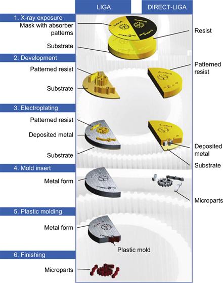
Figure 3.1 LIGA process scheme: a means by which a nickel mold can be formed.
Figure accessed online and adapted from reference [2]. Courtesy Helmholtz-Zentrum Berlin.
3.2 Deep Reactive Ion Etching
Chapter 2 introduced conventional parallel plate dry etching. The application of an electrodeless, high density plasma source using electron cyclotron resonance (ECR) was a breakthrough in dry etching technologies [3]. In Application of Dry Etching to Microsensors, Field Emitters, and Optical Devices, Stella W. Pang states that a Cl2 plasma ignited by an ECR source will produce vertical profiles without the need for side wall passivation [4]. However, the selectivity of SiO2 against Si in the chlorine process is not sufficient. Thin film electrodeposited Ni has a better selectivity but causes stress problems in layers of adequate thickness. Therefore, stress controlled electroplating is performed to increase the mask thickness. Deep reactive ion etching (DRIE), sometimes also called advanced silicon etching (ASE), generally uses inductively coupled plasma systems [5, 6].
Cryo-DRIE is a low temperature process based on fluorine gas that was developed for producing very vertical side walls when anisotropically etching silicon [7, 8]. Optimizing such systems needs increased electron concentrations in the bulk plasma and higher ionization density of reactive species in the dark space (see Chapter 2, Section 2.3.1 for definitions of the mechanisms involved in dry etching). The Bosch process (see Chapter 2) is another example of the use of highly complex plasma equipment in a user-friendly process. The DRIE plasma reactors may be also applied to silica or glass microfabrication. Results of such advanced glass dry etching processes can compete with wet chemical photostructured glass etching (see Chapter 2, Section 2.4.3). Figure 3.2 demonstrates an example in fused silica.

Figure 3.2 Inductively coupled reactive ion etching in silica.
Image courtesy: S. Sukas, University of Twente, 2011.
3.3 Micro-Ceramic Processing
This section has been inspired by the increased interest in the use of ceramic materials in micro- and nanotechnology. Ceramic processing can employ microfabricated molds, and advanced lithographic techniques which allow volumetric up-scaling of the production of ceramic microstructures, such as the LIGA process, can also be applied to ceramics.
The drying conditions and sintering parameters of a number of ceramics are under investigation for micro- and nanomolding applications. The high temperature resistance, chemical inertness, biocompatibility, conductivity, and/or piezoelectric which is a possible property of ceramics make them potentially valuable in applications. Sub-micrometer lateral resolution has been demonstrated for different types of material systems mainly by depositing the ceramic building blocks directly from the vapor phase, e.g., by sputtering into a hard mold.
Ceramic materials may also by shaped by employing ceramic precursor resins in microsterolithography, which is very similar to the microfabrication of plastic microparts (see Section 2.4.5 in Chapter 2). This section gives an introduction to ceramic micro- and nanomolding as an advanced microfabrication processing technology. Such techniques offer efficient and accurate patterning of these otherwise hard-to-process materials.
3.3.1 Micromolding
Microelectronics has been the driving force behind the developments in micro-engineering over the last few decades. The thereof emerging fields such as micromechanics, microoptics, microfluidics etc., have reached consolidation phase in research. In industry, especially telecommunication and medical devices markets have stimulated many new developments at the micro- and nanoscale.
Bioceramics, for example, can be used for repair and reconstruction in the body, and have been extensively investigated for their properties as bioinert or bioactive materials, or because of their ability to form porous structures suitable for tissue ingrowth. Potentially, these materials could interact with tissue at much smaller dimensions if their shape, size and ordering were tightly controlled. Micromolding is known for its vast capability in microfabrication of polymer parts, and generally employs a physical template (called also a mold, stamp or master), which is exposed to the liquified polymer. After hardening, the polymer takes the inverse shape of the mold. This technological strategy is particularly popular because of its large-scale production capabilities: the primary mold structure may be expensive to manufacture, but the costs per part reduce dramatically with replication.
The selection of the mold material and accuracy of the features in the mold define the pattern fidelity in the replication process. Mold manufacture, demolding properties and wear-resistance for the production of polymer microparts has been extensively studied. Various types of lithography can be used to make a mold. Lithography employs a resist layer that is normally polymeric, and sensitive to light of a certain wavelength. The pattern is transferred from mask to resist by an exposure step, from a resist to an underlying functional layer by etching, or from a resist to an added layer by electroplating (or other technique) to form a master structure. Many process sequences are known and several books on the topic are available, for example, Handbook of Microlithography, Micromachining, and Microfabrication edited by Rai-Choudhury [4]. Photolithography may be applied to manufacture a mold in silicon or to transfer a pattern into a metal by electrodeposition. Other means of mold manufacture are available, e.g., laser ablation, micro-electrodischarge machining (Micro-EDM) or even micro-milling.
Micromolding of ceramics can be done either by utilizing advanced gas-phase deposition techniques to fill the mold with a ceramic precursor material, or by simply pouring a ceramic suspension into the mold. This makes large-scale processing also of ceramic microparts possible. Hard as well as soft molds have been investigated for the molding of ceramic materials. A great many ceramic material systems, including hybrids and composites, are possible and will not be part of this overview.
Nanofabrication in ceramic materials has been much reported in the literature, but only a brief insight is presented here. This discussion is based on a review previously published in the journal Small by Auger et al. [9]. Next to silicon micromachining ceramic micromolding could be called a true technology platform, and once it is fully established, many applications may appear. One specific example is the fabrication of microneedle arrays, (see Chapter 8), potentially an ultra-minimally invasive portal to the body for drug delivery and diagnostic purposes.
This chapter introduces ceramic micromolding, demonstrating specifically advanced aspects of this technology.
3.3.2 Ceramic Microparts by LIGA
We have already mentioned that lithographic techniques may be employed for the fabrication of a mold. Although the LIGA process in its original form is not a popular technique, due to the complexity of the light source necessary, the principles involved have often been used for forming a mold for sophisticated, high precision microparts. The tertiary polymer microparts may be filled with metal, or with ceramic fillers. Polymers can be used to provide electrical isolation for the metal structures in a final device, or the polymer structure acts as a lost mold in subsequent high temperature sintering of ceramic microparts. An example of this approach is the use of cements which differ from other ceramic fillers, such as alumina suspensions, in that they set inside the micromold and bond under ambient conditions.
An early example (Colston et al. in 1996), used a LIGA-fabricated nickel mold [10]. This work is influential, since it was the starting point for much materials research. Ordinary Portland Cement (OPC) contains tricalcium silicate as the major component and is used as a model system. The underlying cement chemistry, however, is more complicated in practice; see the original publication for further detail. To improve the final strength, adhesion and permeability of hardened cement, the paste can be modified by polymer additives. The authors of the original paper used styrene butadiene copolymer latex (SBL) as an additional binder between the hydrates and across microcracks and pores. The SBL also contains a surfactant, which enables contact between the hydrophobic polymer mold and the wet cement. Without SBL large cracks develop during hydration causing failure of pattern reproduction. Short hydration times can also increase crack formation. Crack formation during cement micromolding was minimized, and no significant shrinkage was observed when SBL and longer hydration were used. After filling the molds, the cement is cured for up to 16 days and then pyrolyzed within its polymer mold structure from polycarbonate at 400°C for 5 h at ambient pressure. The pyrolysis also burns off the polycarbonate. The polycarbonate lost-mold was formed by the x-ray assisted LIGA method.
Besides demonstrating three different types of cement model systems in this paper, the authors refer only very briefly to the many production variables particle size, choice of latex dispersion, air content, hydrating/curing conditions and parameters of the heating cycle in their concluding remarks. However, these parameters may be better investigated as part of an engineering optimization study, performed if a specific application is considered.
Figure 3.3 illustrates a test feature in OPC after pyrolysis. The structure was hydrated for just 2 days, resulting in a relatively poor reproduction performance, and for 16 days resulting in good replication performance. After long hydration times, the feature contains very detailed, shallow suppressions in the side wall of the ridge structure (originating from the mold made by the LIGA process). The faithful replication of such details in the micro features of a few micro-meters height, illustrates the capabilities of such a process after optimization. A more detailed study can also be found elsewhere [11].
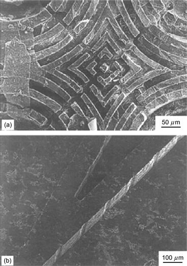
Figure 3.3 Pyrolyzed micromolded features in OPC after 2 days of hydration demonstrating limited reproduction performance (a), and detailed feature of the same design after 16 days of hydration (b).
Reproduced with kind permission from reference [10].
3.3.3 Utilizing Capillaries for Ceramic Micromolding
Micromolding in capillaries (MIMIC) originated from the understanding of microfluidic behaviour in microchannels. Applying the capillary action of microfluidic channels is the key feature of this patterning principle. This discussion centers on its capabilities of patterning ceramic precursors at the microscale, first presented by Kim et al. in 1996 [12]. Figure 3.4 depicts the fabrication process by MIMIC schematically and shows a set of results achieved by this technique with a silica precursor (Accuglass, Allied Signal).
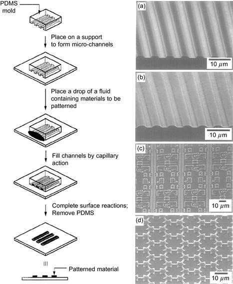
Figure 3.4 Micromolding in capillaries using precursor solution to infiltrate the microcapillaries formed by patterned polydimethylsiloxane (PDMS) confocally pressed against a flat substrate (left) and results of this process in silica (right). Patterns of silica/siloxane on glass by partially converting the precursor to silica at 100°C for 20 min. (a); the same structures in (a) were converted to silica at 425°C for 1 h (b); complex pattern of silica/siloxane on Si/SiO2 (c); and pattern of silica on glass. The precursor film was converted to silica at 425°C for 1 h (d).
Reproduced from reference [12].
A vast amount of research has been carried out in this field, but little progress has been made in industrial applications. It is possible that limited precursor stability causes defects in the produced microstructures making them not yet fit for market. Perhaps MIMIC is better known as a special form of soft lithography, called microfluidic-assisted lithography, and more publications relating to applications may be associated with this term. Ahn et al. studied infiltration kinetics and drying mechanisms during vacuum-assisted microfluidic lithography of colloidal suspensions and fabricated micropatterned ceramic structures by this method [13]. Optimization of the drying conditions of ceramic films is an important aspect of this type of molding process. See also the work of Guillon et al. [14].
Silicon carbide (SiC)-based microelectromechanical systems can operate in harsh environments, for example, as actuators in a combustion chamber. Therefore, Lee et al. demonstrated the patterning of SiC by MIMIC and nanoimprinting, and compared the two different fabrication techniques [15]. This publication is a first attempt to compare ceramic properties when different fabrication processes are used. The MIMIC process uses a hard-PDMS/PDMS composite as a mold. The mold contained lines and spaces in the sub-micrometer range, and was placed onto a clean silicon substrate to form capillaries by conformal contact between the mold and the substrate. A few drops of the ceramic precursor polyvinylsilazane (Ceraset, polysilazane 20, KiON Corp, USA), mixed with a thermal initiator was applied to the entrance of the capillaries. These are filled by the capillary force which is exerted on the droplets. This liquid precursor was cured for at least 6 h at 70°C in a nitrogen atmosphere. Prior to pyrolysis the PDMS mold was dissolved in 1 M tetrabutylammoniumfluoride (TBAF) in tetrahydrofuran (THF) for 20 min. The cured polymeric microstructures were pyrolyzed at 800°C, resulting in a shrinkage of 19% and 39% in width and depth, respectively, but forming a well preserved sub-micron ceramic pattern, which yielded a film strength of up to 60 GPa.
Microcontact printing utilizes also a soft mold from PDMS, transferring material after spinning or inking the mold structure to a substrate. Nagata et al. demonstrated such a type of ceramic printing process for the fabrication of capacitors utilizing stacked BaTiO3 and conducting LaNiO3 thin films [16].
3.3.4 Utilizing Soft-Mold Replication
An example of this is given by Zhu et al. in their work on forming ceramic microgears from a PDMS soft mold. The mold is generated by replication from a primary microstructure which is fabricated by SU-8 thick-film photolithography [17]. The authors used an aqueous alumina suspension containing 1.5 μm high purity Al2O3 particles (Dynamic Ceramic Corp., UK), and Duramex D-3005 (Rohm and Haas, Philadelphia, USA) as a dispersant, and Duramax B-100 and B-1007 were used as binders. The pH of the water-based solution was adjusted by adding NaOH and HCl. The slurry demonstrated best performance at pH 11.
Simple pressurized filling of the microstructures was tested, producing denser ceramic structures. After the green bodies are formed and the binder is removed at 600°C a sinter step with a ramping rate of 200°C/h at 1600°C for 2 h was performed. Figure 3.5 depicts a free-standing microgear with a height and diameter of 1 mm and 2.5 mm, respectively, that was produced in these experiments.
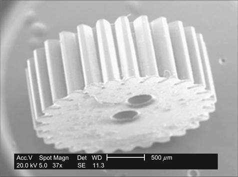
Figure 3.5 Scanning electron micrograph of a sintered ceramic microgear.
Reproduced from [17] with permission from IOP Publishing.
In a subsequent publication, the experiments also used a non-aqueous Al2O3/SiC ceramic suspension, mixed with the commercially available Ceraset Polysilazane 20 (PSZ by KiON Speciality Polymers). This mixture was diluted with acetone (more details of the preparation of the slurry and the curing process can be found in the original publication) [18]. The authors observed that the strong binding force from the cured PSZ prevented both cracking during the drying process, and damage during the demolding step.
3.3.5 Ceramic Patterning on Curved Substrates
This section discusses work by Cannon et al. [19]. The authors first present an extensive overview of the various types of mold being explored for the fabrication of ceramic microparts, and demonstrate ceramic microstructures on curved surfaces for the first time. They also refer to the incorporation of carbon nanotubes in defined sections of the molded ceramic precursor. The combination with nanomaterials is an interesting development, but this text will concentrate on the reported use of flexible PDMS masters to form curved ceramic features which can carry ordered microstructures as small as 20 μm on the inside or outside of a curved surface. These curved surfaces are fabricated by placing the flexible PDMS master with its backing to the curved surface of a macromold (a rod or tube). The micropatterned side is then exposed to the ceramic precursor. The authors used a commercially available low-shrinkage precursor (Cercanam by Ceramatec Inc.) with a composition of greater than 95% alumina with the remaining 5% percent being a proprietary formula. The slurry can be molded or casted into molds with a feature size as small as 5 μm. First the PDMS master is placed onto the curved surfaces with a 3 mm curvature radius. Subsequently, the ceramic precursor is poured onto the molds, and cured by heating at 75°C for 2 h to harden the precursor into a green body. At this stage the green body can be released from the mold, and be cured at 450°C for an additional 2 h. Figure 3.6 illustrates this process. The mold is mounted such that the microstructure is positioned at the outside of the curved surface (Figure 3.6(a) step B). The subsequent replica is therefore inverted, and carries the microstructures in the inside of its curved surface (Figure 3.6(b)), while the details of the features at the microscale are preserved (Figure 3.6(c)).

Figure 3.6 Schematic fabrication process steps A–D (a), and resulting microstructures molded inside ceramic with a curved surface (b) as well as details of the resulting microstructure (c).
Reproduced and rearranged from reference [19] with permission from IOP Publishing.
The ability to micromold ceramics onto a curved surface may impact on the fabrication of complex metal structures by the so-called investment casting method. Flexible PDMS microstructures are transferred into a ceramic structure containing curved as well as microstructured elements. The ceramic part is then filled with, for example, molten aluminum with a melting point of 695°C. The ceramic form is consequently destroyed to form the metal structure, which may then be used as a mold for the production of a large number of polymeric microparts [20].
3.3.6 Patterning Ceramic Materials at Nanoscale Resolution
During the mid 1990s the micromachining community explored many lithographic techniques, to attempt to further reduce the physical dimensions of structures, and so pack more and more functional devices onto an electronic chip with the same area, typically 36 mm × 36 mm. These attempts included self-assembly processes, which involve the deposition of thin films, molecular monolayers, block co-polymers or sub-micrometer sized particles onto a template. The template constrains the position and orientation of the grains or particles, creating highly-ordered features by physically binding the building blocks at pinning points. These pinning points are designed in the template to create hierarchically ordered layers.
The method also provides a certain level of registration for these extremely small features. In some papers this process is called graphoepitaxy, as it is based on the directional solidification of block co-polymer films. Various templating techniques were investigated to produce nanometer-scale parallel patterning of ceramic and organic–inorganic hybrid materials, often based on the soft-lithography approach. A comprehensive review by ten Elshof et al. has summarized these investigations [21].
Auger et al. give an introduction to physical vapor deposition techniques that have been used with templates at the nanometer scale [9]. In this approach the ceramic material itself is directly “molded” (constrained by the template during film growth) instead of its precursors, by using either soft or hard molds, and avoiding the need for post-patterning treatments. To do this the molds must have good anti-sticking properties, achieved by special coatings utilizing so-called surface self-assembled monolayers (SAMs). Silicon molds, for example, have been surface modified by immersion in the SAM precursor, octadecyltrichlorisilane (OTS). Metal molds may be primed by alkanethiolate SAMs to give good anti-sticking properties.
The temperature of the substrate must be controlled during vapor deposition, to ensure that the SAM remains chemisorbed on the surface of the mold. The sensitive SAM layers can be protected by increasing the substrate-target distance and utilization of an inert gas in the sputter chamber. A specific challenge for ceramics is their brittleness, which complicates the demolding process. The thin ceramic films must therefore be backed, for example, by using Scotch® tape or, in a more sophisticated process, by bonding the ceramic film to a glass handling wafer before the demolding step. Free-standing features are therefore difficult to achieve. Auger et al. demonstrated the pattern transfer from a mold containing nanodots for the patterning of AlN, TiN and B4C films [9]. Figure 3.7 illustrates an example of such nanomolded structures.

Figure 3.7 Nanostructured ceramic material patterned by replication. Top-view atomic force microscopy images (1 x 1 μm2) and cross-sectional analysis of the original nanostructures in SiO2/Si (left) and the corresponding nanostructured TiN surface (right).
Reproduced from reference [9].
3.4 Speciality Substrates
3.4.1 Silicon-on-Insulator (SOI)
Silicon wafers have been used abundantly in microelectronics and MEMS as a platform for fabrication. An interesting variation of the standard silicon wafer is the silicon-on-insulator substrate. To produce these wafers two sili- con wafers are bonded together, by using silicon dioxide of approximately 1–2 μm thickness as a bond layer. One of the silicon wafers is thinned down to a thickness of 10–50 μm. The exact layer thickness will depend on the application. Wafer thinning is performed by wet etching so this preparation method is often called the bonding-and-etchback technique. The buried oxide layer (BOX) is not accessible unless bulk micromachining is performed, either on the thinned top or full thickness silicon wafer, which also acts as a handling platform for processing. Alternatively, a special cracking technique involving hydrogen implantation, bonding and heating of the wafer stack to 470°C can be used to create a thin silicon wafer on top of the BOX layer. Bonding of a 300 μm quartz wafer sandwiched between two standard 525 μm thick silicon wafers was also demonstrated [22].
These speciality substrates find applications in power electronics, electronic operations for application at elevated temperatures, bulk micromachined xyz-stages, radio frequency (RF-MEMS) switches, microheater devices for microfluidic applications and integrated optical systems.
3.4.2 Electro-Optic Substrates
Another group of speciality substrates are materials that carry the electro-optical effect, for example, LiNbO3 [23]. These types of materials are important for the design of so-called surface acoustic wave (SAW) devices. In the ferroelectric LiNbO3 and other SAW device materials SAWs are excited by interdigitated metallic finger electrodes, which are fabricated by depositing a thin metal layer (gold, aluminum) on the substrate surface and lithography. These devices form electronic filter and signal delay lines and are mainly manufactured for television and mobile communication applications. SAW devices therefore represent a huge market.
3.5 Advanced Non-Silicon and Silicon Hybrid Devices
The selection of a specific material at the component level is based on its unique properties (e.g., optical, piezoelectric, magnetic, super-strong, lightweight, self-cleaning, shape-memory and other smart properties). Integration of these materials with other integrated components, specifically electronic devices, can be highly challenging. One of the preferred solutions is to process the components in different production lines, and merge them at some stage of back-end processing to generate a hybrid integrated system. The following two subsections will give brief examples of such approaches.
3.5.1 Nanofabrication of Information Storage Devices
One of the early adaptors of nanotechnology is the data storage media market. Technical developments in the fields of optical and magnetic data storage media have been adopted at an extremely high pace. Research findings from as recently as 10 years ago are currently being tested for application and there is no doubt that this industry will grow further.
Nanotechnology plays an evermore important role in information storage. The need in the market for functional elements that approach the physical limit of so-called patterned media that have dot dimensions and pitches of the order of a few nanometres is an enormous driver for research and development in this area. Below this limit, thermal noise dominates and the distinguishable writing and reading of a single dot becomes impossible. At the same time research continues to explore other means of information storage, e.g., in the capture and release of energy through chemical bonds in single molecules. We will discuss examples of the fabrication of patterned magnetic media in Chapter 4, which covers nanofabrication.
3.5.2 Integrated Optics
Optical devices and systems, such as CD-ROMs, DVDs, and TFT image displays, are part of our daily lives, both at home and on the move. A vast amount of information can be easily accessed anywhere via the World Wide Web, by devices such as PCs and mobile telephones. The business impact of this type of development was cited in market research reports that claimed extremely high growth rates for the fibre-integrated market sector between 1999 to 2003 due to the huge increase in commercial and public use of the internet [24].
This technology has made an enormous impact on our lives regardless of its commercial success. Also we now know that economic welfare and flourishing, sustainable businesses are probably more closely linked to a stable banking system than sole technical innovation.
The introduction of micro components has revolutionized the entire field of photonics. Optical phenomena depend on the careful alignment of all system components, which could not be realized in traditional bulk free space optics. Because free space optic components are usually mounted on optical benches, system operation degrades due to ambient variations, which still demands further research and development.
New research has, however, resulted in the idea of micro-optical benches, so converting the optical system into a compact, stable (vibration tolerant) package [25–27]. Early work in photonic device development followed the same approach as planar thin film technologies, producing opto-electronics components. But the need soon arose for optical modulation, beam steering and input/output coupling of three-dimensional, actuated micro-optical switch devices, such as the one depicted in Figure 3.8 [28]. This category of device belongs to the novel field of photonics devices that was founded on developments in MST/MEMS technology, and so they are named micro-opto-electromechanical systems (MOEMS).

Another example in this field which clearly demonstrates the technology gap between scientific research and final development is the semiconductor laser. Although predicted in the late 1950s and developed around 1960, the commercialization of laser diodes did not start before the early 1980s [29]. It appears equally difficult to bridge this technology gap in MEMS developments, although some preliminary commercial success was achieved during the dot-com era. Economic losses in this period are in no way related to a lack of technical possibilities, but investments could have been more selective at that time.
On the other hand thin-film related optical integration has steadily increased over recent years, and is clearly currently better suited to industrial applications than are free space micro-optics. The next section will give examples of important developments in the field of planar integrated optics.
3.6 Planar Lightwave Circuits
A difference in optical refractive index between two materials can be used to guide photons. The optical fibre cable is the most efficient long distance information carrier that we currently know, with transmissions reaching an optical loss of less than 0.4 dB/km at 1.3 μm [30]. The advantage of a circular fibre is its extremely sharp transition from the core to the cladding. Pulling the core from a master means that the core is embedded into the cladding with a very smooth surface [31]. This degree of side wall smoothness and radial symmetry is difficult to achieve using planar patterning methods. The higher the roughness of the encapsulated surfaces, the higher is the optical power loss. When fabricating planar optical circuits, similar requirements to the fibre cable are expected. A highly optically homogeneous material must be shaped into a guiding device. For slab waveguides, this problem is to do with the surface quality of the substrate and the grain properties (morphology) of the deposited layer. However, in channel guides, optical transmission is also restricted by losses through the side walls. This roughness must be reduced to produce a device of the required standard, and to do this, an appropriate technique used to pattern the waveguide. Patterning methods can be divided into three groups:
1. subtractive pattern transfer through a masking layer,
2. additive processing by lift-off, or
3. selective change of refractive index, for example, by doping.
Refractive index modulation relies on either diffusion at high temperature, ion exchange or high energy ion implantation. Very sophisticated features can be made by pulsed laser techniques, which may be also suitable for selectively changing material properties and therefore being suitable for direct writing of waveguide devices [32, 33]. Refractive index control and the transition towards the cladding layer are non-trivial in all of the three techniques listed above. The easiest approach is the deposition of a highly homogeneous film of defined thickness and refractive index onto a substrate and then etching away the excess material to create the guide structure.
The optically guiding layer on the substrate is called a slab waveguide, and they are the building blocks of optical devices which are used to confine information in the optical frequency domain and transfer the energy traveling along the surface-defined optical layer. Optical tracks can be embedded in the substrate by splitting and merging these guiding tracks in a similar way to electronic circuitry. Hence these devices are referred to as planar lightwave circuits (PLCs). The optical material may be deposited in layers from solution, applied by spin-coating, or by dielectric film deposition techniques such as flame hydrolysis, chemical vapor deposition or sputtering. However, to achieve a 3D channel, the lateral dimensions of the material must be defined, too. This waveguiding effect is sensitive to roughness as discussed above. Scattering on a rough surface creates optical loss and inhibits the achievement of high quality guiding properties. Optical loss is also caused by curved side wall profiles.
Wet chemical etching has only limited use for producing channel waveguides. The high specifications of photonics call for specific fabrication processes in suitable materials and with high pattern fidelity with respect to the optical functionality. Other applicable techniques are doping by diffusion, ion beam implantation or ion exchange, but the resolution of these techniques is limited [30, 34]. Dry etch processes can compensate for the disadvantages of wet etching and produce high resolution structures. Selecting the exact sequence of the process steps requires a detailed knowledge of material properties, and hence must be altered for each material.
Although novel photonic crystal materials have been introduced, most industrial devices are made by combinations of bulk and surface silicon micromachining as well as hybrid assembly of active optical and waveguiding components by lithography. The lift-off process could also be capable of attaining the required side wall quality if precise lithographic control and very thin films are used. Use of lift-off techniques with polymer masks does, however, restrict the process temperature to around 200°C. In light of these arguments, the removal of the unwanted materials via dry etching appears to be the most feasible approach.
Many waveguide processing protocols integrated with micromechanical devices have been developed in university-based research groups. For example, at the Optical and Semiconductor Devices Group, Imperial College, London, UK, an in-house RIE process for silicon dioxide etching has been developed, which consists the following steps:
1. Thermal dry oxidation of the silicon wafer at 1100°C for 24 h;
2. Sputtering of a Cr-layer to act as mask material;
3. Cr-mask patterning by photolithography and wet etching in a standard Cr-etchant;
5. Silica dry etching in CHF3/Ar/O2 gas mixture through Cr-mask, etch rate: 50 nm/min (experimental result for Plasma Technologies RIE 80 equipment).
In general, surface micromachining is considered important to the development of micro-opto-mechanical integrated sensor devices and is often described in the literature, specifically with respect to the patterning of waveguides [35, 36]. Wet and dry processes have advantages and disadvantages for making channel waveguides. The processing techniques used in integrated optics are so similar to the processes of very-large-scale integration (VLSI) microelectronic techniques that they will not be described in detail here. Instead, we give an overview of optical specifications for waveguides and their manufacturing techniques, either applied or considered in the design methodology of sensors and actuators. Fundamental information about the fabrication of integrated planar optical devices can be found elsewhere [30, 37, 38].
TiO2, Ta2O5, Al2O3, Si3N4 and SiOxNy are some of the most common materials for visible light (633 nm) waveguides on glass or silica-on-silicon substrates. To minimize the optical power required to illuminate the target and retrieve a signal from the scattered light in the case of scanner devices, the loss of the waveguide structure should be made as low as possible. This optimization can be addressed by an index difference between core and cladding (or buffer) of at least greater than 1% (specifically for silicon-based optical integration a higher degree of index difference is preferred). The overall length of a straight waveguide will determine the attenuation allowed (for integrated sensing devices, a length of 15–25 mm is probably sufficient), i.e. higher levels of loss may be accepted for these relatively short guides. The surface and side wall roughness should be as small as possible, e.g., a roughness value as low as 5 nm rms could already convert 10% of the fundamental mode into higher mode energy, which cannot propagate along the core for more than one meter, although the effect is wavelength dependent [31]. The roughness/shape of the end face, which is often used for coupling to the light source, determines the coupling loss. If a waveguide is used to illuminate a sample, the roughness/shape of the waveguide ending will determine illumination properties, such as resolution, intensity and stray light loss.
Finally, the intrinsic microstructure of the material itself is important. Layers with small grain size and low porosity will reduce the attenuation of the propagated waves. The choice of a substrate material is also important. Silicon, for example, has a very high refractive index (3.4). To provide a guide for light in the visible range, the waveguide core has to be isolated from the substrate to avoid leakage of energy. Planar silica-on-silicon light circuits are made possible by applying fairly thick optical buffers, which prevent guided modes from coupling into the substrate. This allows the realization of low-loss waveguides on silicon. Figure 3.9 compares the refractive indices of differently deposited materials with the index of selected substrates.
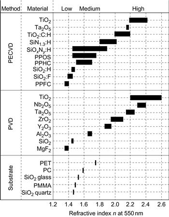
Figure 3.9 Refractive indices (at λ = 550 nm) of optical thin films.
Reproduced from reference [39].
The optical buffer layer between the waveguide core and the substrate must have an appropriate thickness. Figure 3.10 shows the relationship between buffer layer thickness and the thickness of the waveguide layer as it relates to the refractive index of the guiding material [37]. The graph demonstrates that for single mode light propagation with a layer thickness of approximately 0.3 μm and a refractive index of 1.7 at λ = 633 nm, the thickness of the buffer must exceed 1 μm.

In most cases an amorphous glass film is a suitable material for optical waveguides in the visible wavelength range. The amorphous films are deposited onto glass substrates, which are also amorphous (e.g., fused silica and thermally grown silica buffer layers on silicon wafers) [40]. In general, any substrate with a smaller refractive index than the guiding layer should provide some degree of light transmission. In addition, single-crystal films can be grown via epitaxial techniques onto a single-crystalline substrate, if the lattice constants of both the film and the substrate are closely matched.
Epitaxial growth is widely applied in optoelectronic device fabrication. For example, Kim and Yoon have studied ZnO/InP heterostructures [41]. The work describes the epitaxial film growth of ZnO on InP substrates using low temperature rf-magnetron sputtering, which is of considerable interest for optoelectronic devices. The paper reports on the material properties characterized by atomic force microscopy (AFM), Auger electron spectroscopy (AES) and transmission electron microscopy (TEM). The equipment used is not described further, but a review of optical film technology can be found in Martinu and Poitras [39].
Polymers can also be used as waveguiding layers. Organic materials are, however, more difficult to incorporate into a post-processed substrate. Such a substrate might carry fragile electromechanical features and therefore place higher demands on the polymer coating technique than a planar substrate. Dip coating and plasma polymerization are alternatives to the commonly applied spin-coating technique. The simple application of polymers, via spin-on methods on bare substrates, have produced remarkable results, but this approach has not yet been widely used for applications [42–44].
Silica-on-silicon has produced good quality planar waveguide circuits and can be produced prior to bulk-etch processing [45]. Materials such as silicon nitride are well known from passivation or masking layers in microtechnology and are highly stable, hence they have been thoroughly investigated as guiding layers because they allow refractive index tuning over a wide range (see Figure 3.9). They can also be deposited in very short periods of time (a few minutes for PECVD) compared to sputtered metal oxides, which are deposited at a much lower pressure region and require pumping times of up to several hours, although material deposition rates may be comparable to CVD processes.
Deposition technology at low temperature has been also developed by applying a photo-CVD process. Such photo-assisted deposition uses xenon or krypton chloride excimer lamps to provide energy for the chemical reaction [46]. TiO2 as well as (Ta2O5)1-x(TiO2)x on silicon has been reported [47, 48]. Table 3.1 compares the characteristics and film properties of the various processes.
Table 3.1 Optical thin films and their deposition processes

3.7 Fabrication Example of an Integrated Optical Device
The aforementioned techniques for processing waveguides are currently widely available for their integration into sensor devices. This section presents the application of these fabrication methods to integrating optical waveguide sensors with an active optical function. Both light generation and light detection rely on semiconductors. As mentioned previously, the pure transmission of light can be realized with passive materials, such as amorphous glasses.
Dry etching in a gaseous atmosphere at low pressure is the method of choice for the industrial production of waveguide features. This process can be integrated into standard microelectronic circuit manufacture as post- or pre-process to the so-called complementary metal oxide semiconductor (CMOS) technology. Besides the higher accuracy that is achieved by dry etching, it is also compatible with CMOS, which often only allows post-process integration.
Several types of dry patterning equipment are available. Sputter systems are the oldest; originally operated in a back-etch mode to clean the substrate surface prior to thin-film deposition. Most processes for optical waveguide etching currently use a dedicated reactive ion etcher (RIE), as described in Chapter 2 for silicon etching. For reactive ion etching of waveguides, the gas must be carefully chosen to yield high pattern fidelity at a high etch rate (selectivity) for the waveguide material against the optical buffer layer.
Section 3.6 introduced a wide variety of materials used for optics integration. Etch parameters are very dependent on the exact composition of the material and its film morphology as well as machine conditions. Often deposits at the reactor wall can influence and disturb subsequent processes. One example of a specific waveguide design is the integrated Mach–Zehnder interferometer depicted in Figure 3.11. These interferometers have been demonstrated in a variety of applications, such as modulators, couplers and sensors. They can be also integrated with micromechanical sensors to read a mechanical measurement signal [54, 55].

Figure 3.11 Wavelength and polarization insensitive integrated directional coupler using Mach–Zehnder structures. Parameters used to model the device performance are: Δn/n = 0.3%, λ = 1550 nm, polarization TE (transverse electric).
Figure redrawn from reference [56], with permission by Dr. Thomas E. Murphy, Photonics Research Laboratory, University of Maryland, USA
Figure 3.11 shows the schematic principle of the waveguide design and the etched channel waveguide achieved in a Germanium-doped silica layer on top of a silica buffer layer of 20 μm thickness. The integrated optical device is fabricated using the process sequence given in detail in Figure 3.12. This type of device contains critical curved elements that not only require smooth side walls, but also a sophisticated layout during manufacture of the electron-beam-patterned photomask. Frequently, photomasks suffer from raster steps in the case of shaping the vector scan of the electron beam along the curved segments of the design. This effect results from the way the pattern generator operates; thus the mask fabrication process for curved optical elements has to be optimized for side wall roughness. In general, Gaussian electron beam lithography is preferred for the generation of photomasks containing micro-optical features.
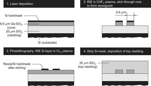
Figure 3.12 Processing sequence of advanced waveguide device.
Figure redrawn from reference [56], with permission by Dr. Thomas E. Murphy, Photonics Research Laboratory, University of Maryland, USA
3.8 Integrated Optics in the MST Foundry Service Industry: A Case Study
The processes described in Section 3.7 can be supplied by a MST foundry. Examples of services to supply such micro parts can be found on the internet, one of which is described below. LioniX BV is a spin-off company of the MESA+ Institute for Nanotechnology, University of Twente, Enschede, The Netherlands. LioniX provides their customers with product development stage and production services. They are well-known as an optical MST/MEMS foundry, and a leading provider of small to high volume production services of highly innovative products. The company often takes the position of a technology developer, carrying on developments that originated from research. Bringing such ideas to commercialization requires a distinct skill set. Similar to the concept of a conveyor belt, LioniX can sustain this complex pathway from idea to industry.
Facilitating technology transfer from the academic to the industrial domain plays a large role in the success of high-tech innovation, and LioniX cooperates with their clients and partners through subcontracting, licensing of IP or joint ventures. One example is the integration of optical read-out functionality in biosensors, which was originally developed by the University of Twente [36]. The heart of such a sensor is a Mach–Zehnder interferometer, similar to the design illustrated in Figure 3.11. The portable design of the integrated sensor is its unique selling point.
These sensors may be applied in food or environmental sensing, but higher economical margins may be gained for such an advanced sensor design in the health care market. An outline application is presented in Figure 3.13, and the concept has been published in various scientific journals. The figure is reprinted from Nano Letters, Ymeti et al. [57]. More information concerning LioniX foundry services may be found from the company’s website [58].
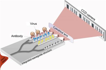
Figure 3.13 Illustration of an integrated optical sensor concept.
Reproduced with permission from reference [57].
3.9 Conclusions
Micro- and nanomolding technology for ceramic and organic–inorganic hybrid materials is an emerging field that can be applied to make devices with specific properties including, for example, extreme chemical inertness, bioactivity or high temperature resistance. Many materials are currently being investigated, particularly fused silica and compound semiconductors, which can be used for many optical devices [59–61]. Patterning by RIE is the fabrication method of choice, although many micro- and nanomolding processes are discussed in the literature.
Most of the processes described in this chapter are based on soft molds utilizing PDMS and precursor suspensions. However, techniques such as LIGA and DRIE were highlighted before moving towards more detailed descriptions. In certain applications the use of a hard mold instead of the flexible PDMS may offer certain benefits in production processes, and silicon and replicated polycarbonate have been used. Micromolding in capillaries is discussed, as it may present a particularly promising method for the exploration of functions facilitated by the extensive tailorability of ceramic and organic–inorganic hybrid materials. Micro- and nanomolds can be fabricated by many techniques, including milling, and time- and cost-consuming focused electron and ion beam processes, but generally lithographic processes are needed to produce a high resolution.
One popular lithographic technique is photolithography using SU-8 thick film resist. Using these pre-patterned micromachined silicon wafers allows complex shapes to be realized, such as microneedles. These structures can be used as a master to form a production mold for a subsequent replication process in ceramics.
In all ceramic microprocesses that use precursors, the suspension’s composition, drying and sintering conditions will all affect the result of the ceramic molding process. Pressurized filling and long hydration times can improve the results. Ceramic fillers from suspensions suffer from a certain amount of shrinkage, but physical vapor deposition of the ceramic building blocks produces no shrinkage. Self-assembling monolayers were used as anti-sticking layers to allow separation of the hard mold from the ceramic film after deposition. However, the ceramic films may be extremely brittle and may be damaged by demolding, so a backing layer needs to be applied to release the films from the mold. Soft mold replication is easier and allows patterning on curved surfaces due to its flexibility. Soft lithography has already proved to be an outstanding alternative method to conventional techniques. Ceramic materials can be patterned at the nanoscale using this approach, if high temperature treatments are avoided after demolding, since these lead to reflow and shrinkage.
With respect to applications, the tunable porosity of ceramics may offer additional advantages compared to other materials allowing, for example, tissue ingrowth and controlled release of drugs.
Surface micromachining has influenced the rapid rise of optical micro-optical-electromechanical systems (MOEMS). Planar processed features, like mirrors, shutters or Fresnel lenses can be assembled into 3D devices to generate novel MOEMS [27, 62]. The fabrication of optical devices, including waveguides, relies on the same principles as polysilicon surface technology. To minimize optical loss (from attenuation and scattering) in channel waveguides, the fabrication method is closely controlled for good side wall definition of the resist patterning process, and low surface and side wall roughness. Certain optical slab materials may confer a higher etch selectivity using hard masks instead of a polymer (resist) layer. Because these hard masks must be patterned, too, the number of process steps is increased, which could lead to a higher failure rate across the entire process sequence.
In conclusion, we have introduced the processing of speciality substrates, and the concepts involved in the fabrication of integrated lightwave circuits and sensors. We have also briefly discussed the industrial scope of optical integrated microsystems and their applications. In this context, an example of a successful MST foundry service – an illustration of effective technology transfer from universities to the market place – has been presented.
REFERENCES
1. Feiertag G, Ehrfeld W, Freimuth H, et al. Fabrication of photonic crystals by deep x-ray lithography. Appl Phys Lett. 1997;71(11):1441–1443.
2. LIGA – Our Key Technology, Helmholtz Zeutrum Berlin, http://www.helmholtz-berlin.de/forschung/grossgeraete/azm/hzb-intern/verfahren_en.html (accessed 04.04.11).
3. Boswell RW, Perry AJ, Emami M. Multiple confined diffusion plasma produced by 13.56 MHz electrodeless source. J Vac Sci Technol A. 1989;7(6):3345–3350.
4. Pang S. Application of dry etching to microsensors, field emitters, and optical devices. In: Rai-Choudhury P, ed. Monograph PM40 Washington: SPIE Optical Engineering Press; 1997;99–152. Handbook of Microlithography, Micromachining, and Microfabrication. vol. 2 Ch. 3, ISBN: 0-8194-2379-3(v.2].
5. Keller JH. New and possible future trends in inductively coupled plasmas (ICPs) for semiconductor processing. Plasma Phys Control Fusion. 1997;39(5A):437–443 Spec. Iss.
6. McAuley SA, Ashraf H, Atabo L, et al. Silicon micromachining using a high-density plasma source. J Phys D-Appl Phys. 2001;34(18):2769–2774.
7. Hynes AM, Ashraf H, Bhardwaj JK, Hopkins J, Johnston I, Shepherd JN. Recent advances in silicon etching for MEMS using the ASETM process. Sens Actuators. 1999;74:13–17.
8. de Boer MJ, Gardeniers JGE, Jansen HV, et al. Guidelines for etching silicon MEMS structures using fluorine high-density plasmas at cryogenic temperatures. J Microelectromech Syst. 2002;11(4):385.
9. Auger MA, Schilardi PL, Caretti I, et al. Molding and replication of ceramic surfaces with nanoscale resolution. Small. 2005;1:300–309.
10. Colston SL, Barnes P, Freimuth H, Lacher M, Ehrfeld W. Cements: A new medium for micro-engineering structures?. J Mater Sci Lett. 1996;15:1660–1663.
11. Colston SL, O’Connor D, Barnes P, et al. Functional micro-concrete: The incorporation of zeolites and inorganic nano-particles into cement micro-structures. J Mater Sci Lett. 2000;19(12):1085–1088.
12. Kim E, Xia Y, Whitesides GM. Micromolding in capillaries: Applications in material sciences. J Am Ceram Soc. 1996;118:5722–5731.
13. Ahn S-J, Min JH, Kim J, Moon J. Process mechanism for vacuum-assisted microfluidics lithography with ceramic colloidal suspensions. J Am Ceram Soc. 2008;91:2143–2149.
14. Guillon O, Jamin C, Bordia RK. Effect of drying conditions on patterned ceramic films processed by soft micromolding. J Ceram Soc Jpn. 2010;118:321–325.
15. Lee D-H, Park K-H, Hong L-Y, Kim D-P. SiCN ceramic patterns fabricated by soft lithography techniques. Sens Actuators A: Phys. 2007;135:895–901.
16. Nagata H, Ko SW, Hong E, Randall CA, Trolier-McKinstry S. Microcontact printed BaTiO3 and LaNiO3 thin films for capacitors. J Am Ceram Soc. 2006;89:2816–2821.
17. Zhu Z, Wei X, Jiang K. A net-shape fabrication process of alumina micro-components using a soft lithography technique. J Micromech Micro Eng. 2007;17:193–198.
18. Zhu Z, Hassanin H, Jiang K. A soft moulding process for manufacture of net-shape ceramic microcomponents. Int J Adv Manuf Technol. 2010;47:147–152.
19. Cannon AH, Allen AC, Graham S, King WP. Molding ceramic microstructures on flat and curved surfaces with and without embedded carbon nanotubes. J Micromech Micro Eng. 2006;16:2554–2563.
20. Cannon AH, King WP. Microstructured metal molds fabricated via investment casting. J Micromech Micro Eng. 2010;20:025025 [7pp].
21. ten Elshof JE, Göbel OF, Kahn SU. Micrometer and nanometer-scale parallel patterning of ceramic and organic–inorganic hybrid materials. J Eur Ceram Soc. 2010;30:1555–1577.
22. Lee TH, Tong QY, Chao YL, Huang LJ, Gösele U. Silicon on quartz by a smart cut process. In: Chrisstoloveanu S, ed. Proceedings of the 8th International Symposium on Silicon-on-Insulator Technology and Devices. Pennington, NJ: The Electrochemcial Society; 1997;27–32.
23. Takagaki Y, Wiebicke E, Kostial H, Ploog KH. Fabrication of GHz-range surface-acoustic-wave transducers on LiNbO3 using imprint lithography. Nanotechnology. 2002;13:15–17.
24. ATIP document id: 010821ar attip01.038: MOEMS for telecommunications in europe. http://www.atip.org/atip-publications/atip-reports/2001/7354-atip01-038-moems-fortelecommunication-in-europe.html, 2001 (accessed 19.06.11).
25. Syms RRA. Surface tension powered self-assembly of 3-D micro-optomechanical structures. J Microelectromech Syst. 1999;8:448–455.
26. Lin LY, Shen JL, Lee SS, Su GD, Wu MC. Microactuated micro-XYZ stages for free-space micro-optical bench. In: MEMS97, Proceedings, IEEE, 10th Annual International Workshop on Micro Electro Mechanical Systems. 1997;43–48.
27. Wu MC, Lin L-Y, Pister KSJ, Lee S-S. Micromachined free-space integrated micro-optics. Sens Actuators A: Phys. 1995;50(1–2):127–134.
28. Giles CR, Bishop DJ, Aksyuk V. MEMS for light-wave networks. MRS Bull. 2001;26:328–329.
29. Sawada R, Higurashi E, Ito T. Highly accurate and quick bonding of a laser-diode chip onto a planar lightwave circuit. Prec Eng J Int Soc Prec Eng Nanotechnol. 2001;25:293–300.
30. Hunsperger RG. Integrated Optics Berlin: Springer; 1995.
31. Gloge D. Optical waveguide transmission. Proc IEEE58 1970;1513–1522.
32. Ihlemann J, Schäfer D. Fabrication of diffractive phase elements for the UV-range by laser ablation patterning of dielectric layers. Appl Surf Sci. 2002;197–198:856–861.
33. Krishnan R, Lisfi A, Guyot M, Cagan V. Preparation and some properties of pulsed laser deposited YFeO3 films. J Magn Magn Mater. 1995;147(3):221–224.
34. Nolan DA, Bhagavatula VA, Lerminiaux C. Integrated-optics planar components. IEEE Commun Mag. 1994;32:62–67.
35. Wärhof K, Driessen A, Lambeck PV, Hilderink LTH, Linders PWC, Popma ThJA. Plasma enhanced chemical vapor deposition silicon oxynitride optimized for application in integrated optics. Sens Actuators A. 1999;74(1–3):9–12.
36. Heideman RG, Lambeck PV. Remote opto-chemical sensing with extreme sensitivity: Design, fabrication and performance of a pigtailed integrated optical phase-modulated Mach–Zehnder interferometer system. Sens Actuators B. 1999;61:100127.
37. Nishihara H, Haruna M, Suhara T. Optical Integrated Circuits New York: McGraw Hill; 2000.
38. Tamir T, ed. Integrated Optics. Berlin: Springer; 1979.
39. Martinu L, Poitras D. Plasma deposition of optical films and coating: A review. J Vac Sci Technol A. 2000;18(6):2619–2649.
40. Beltrami DR, Love D, Durandet A, Samo A, Cogswell CJ. Fabrication and characterization of a planar gradient-index, plasma-enhanced chemical vapor deposition lens. Appl Opt. 1997;36(28):7143–7149.
41. Kim TW, Yoon YS. Microstructural properties of ZnO epitaxial films grown on p-InP (100) substrates at low temperature. J Cryst Growth. 2000;212:411–415.
42. Bosc D, Devoldère N, Bonnel M, Favennec JL, Pavy D. Hybrid silica–polymer structure for integrated optical waveguides with new potentialities. Mater Sci Eng B. 1999;57:155–160.
43. Darraud-Taupiac C, Binsangou V, Decossas JL, Vareille JC. Optical waveguides fabricated on polymer substrates by electron beam. Mater Sci Semicond Process. 2000;3(5):363–365.
44. Kim JH, Kim EJ, Choi HC, et al. Evaluation of fluorinated polyimide etching processes for optical waveguide fabrication. Thin Solid Films. 1999;341:192–195.
45. Kawachi M. Recent progress in silica-based planar lightwave circuits on silicon. IEEE Proc Optoelectron. 1996;143(5):257–262.
46. Vossen JL, Kern W. Thin Film Processes II New York: Academic Press; 1991.
47. Kaliwoh N, Zhang JY, Boyd IW. Titanium dioxide films prepared by photo-induced sol-gel processing using 172 nm excimer lamps. Surf Coat Technol. 2000;125(1–3):424–427.
48. S.P. Lansley, Diamond photodetctor for deep ultra-violet applications, PhD thesis, University College, University of London, UK, 2001.
49. Cheng S-D, Zhou Y, Kam CH, et al. Sol-gel derived thin films of LiTaO3 on SiO2/Si substrates for optical waveguide applications. Fiber Integr Opt. 2001;20:45–52.
50. Huttel I, Gurovic J, Cerny F, Pospisil J. Carbon and carbon nitride planar waveguides on silicon substrates. Diam Relat Mater. 1999;8(2):628–630.
51. M.K. Smit, Integrated optics in silicon-based aluminum oxide, PhD thesis, Delft University of Technology, Delft, The Netherlands, 1991.
52. Zhang J, Ren Z, Liang R, Sui Y, Liu W. Planar optical waveguide thin films grown by microwave ECR PECVD. Surf Coat Technol. 2000;131(1):116–120.
53. de Ridder RM, Wijbrans RA, Albers H, et al. A spot-size transformer for fiber-chip coupling in sensor applications at 633 nm in silicon oxynitride. In: LEOS’95 Annual Meeting. 1995.
54. Nathan A, Bhatnagar Y, Vadekar A, Huang W. Fabrication of a silicon Mach–Zehnder interferometer for mechanical measurands. In: Waterloo, Ontario, Canada: University of Waterloo; 1993;19–26. Proceedings of SPIE - The International Society for Optical Engineering. vol. 1793.
55. Benaissa K, Nathan A. Silicon anti-resonant reflecting optical waveguides for sensor applications. Sens Actuators A: Phys. 1998;65(1):33–44.
56. T.E. Murphy, Design, Fabrication and Measurement of Integrated Bragg Grating Optical Filters, PhD thesis, Massachusetts Institute of Technology, 2001, © Massachusetts Institute of Technology, 2001, Chapter 3, pp. 108–120.
57. Ymeti A, Greve J, Lambeck PV, et al. Fast, ultrasensitive virus detection using a young interferometer sensor. Nano Lett. 2007;7(2):394–397.
58. Home page of LioniX. www.lionixbv.com, (accessed 04.04.11).
59. Shul RJ, McClellan GB, Briggs RD, et al. High-density plasma etching of compound semiconductors. J Vac Sci Technol A – Vac Surf Films. 1997;15(3):633–637.
60. Shul RJ, Vawter GA, Willison CG, et al. Comparison of plasma etch techniques for III-V nitrides. Solid-State Electron. 1998;42(12):2259–2267.
61. Schaepkens M, Oehrlein GS. A review of SiO2 etching studies in inductively coupled fluorocarbon plasmas. J Electrochem Soc. 2001;148(3):C211–C221.
62. Tien NC. Micro-optical inertial sensors using silicon MEMS. In: Proceedings of the Aerospace Conference. Piscataway, NJ, USA: IEEE; 1998;437–443. vol. 1.