
Chapter 2
Basic Technologies for Microsystems
Chapter Contents
2.1 Photolithography
2.2 Thin Films
2.2.1 Wet Deposition Techniques
2.2.2 Vapor Deposition Techniques
2.3 Silicon Micromachining
2.3.1 Etching
2.3.2 Surface Micromachining
2.3.3 Silicon Bulk Micromachining
Anisotropic Wet Chemical Etching
2.4 Industrially Established Non-Silicon Processing
2.4.1 Quartz Etching
2.4.2 Glass Wet Etching
2.4.3 Photostructurable Glass
2.4.4 Powder Blasting
2.4.5 Plastic Microfabrication
2.5 Conclusions
This chapter aims to make the reader comfortable with the tremendous amount of fabrication techniques that have found their way into applications since the onset of microtechnology in the 1950s and 1960s. Although there exist many excellent texts and reviews on the art of microfabrication, this chapter also introduces the reader to the nomenclature of micro- and nano- fabrication techniques as used in the remainder of the book and in science and industry.
Although many of the processes in use were initially derived from microelectronics, design engineers quickly realized that this approach restricts the possibilities for mechanical, optical, chemical and biological functionality. Hence, this chapter starts with an explanation of the primary techniques that were first performed with silicon and then moves on to the technologies which allow the use of other materials. The introduction of new materials has demanded the development of new microfabrication techniques, which we like to refer to as advanced microfabrication technologies. These are described in the next chapter. However, an introduction to non-silicon-specific techniques is given here, too. Furthermore, processing and application examples of the basic techniques are illustrated in a set of selected references.
2.1 Photolithography
Lithography generally involves the transfer of a pattern from a master into a pattern transfer layer, the resist, which is then used for subsequent pattern transfer onto a working surface, e.g., silicon. There are several different lithographic pattern techniques, of which photolithography is the most common.
This technique uses a resist layer that is sensitive to ultra-violet light. Accordingly, the light source is an ultra-violet (UV) source, which illuminates the resist through a specific master. The light spectrum of a mercury lamp has a UV peak at 365 nm. Combining a mercury light source with the necessary tooling for holding and moving the master (the mask) in a precisely defined way against the working surface allows the patterns to be aligned very closely. This combination of optics, precision engineering, and sensory control and feedback has resulted in one of the most essential production apparatuses of the microelectronic industry. They are known as mask aligners and are provided by specialist manufacturers. ASML, which is based in the Netherlands, is one such company. Any microfabrication process starts with a work piece, called the substrate or wafer, which may only serve as a handling platform, or may become a part of the integral device design. Wafers can be made from different materials, of which silicon is the most established.
During lithography, the resist, a polymer-based, light-sensitive compound of defined viscosity, is deposited onto the wafer. This may be performed simply by dispensing a puddle of solvent-dissolved resist onto the surface of the wafer and then rotating the wafer at high speed (spin-coating). The initial acceleration, reached speed, spin time and viscosity of the resist will define the thickness and uniformity of the coating on the wafer after the solvent has evaporated. Upon exposure to the light source, the molecules in the resist either cross-link (negative tone resist) or undergo scission (positive tone resist). The latter is often preferred because of the direct relationship between exposure intensity and rate of dissolution in the subsequent development step. These two processes of exposure and development are very similar to the same processes in photography. Negative tone resist requires an additional catalytical reaction, which is often initiated and accelerated by a moderate increase in temperature, making this resist system more complex. However, both types are widely used, with selection depending on the specific purpose the resist layer has to serve in the processing sequence.
There are a number of resist materials available commercially. The term ‘resist’ is used because this layer is used as a masking layer for the next etching or deposition. Hence, the resist allows the removal or addition of material to or from a specific region of the wafer. In the case of an additive process, the resist will be dissolved and carry the deposited layer from these regions with it. This process is called a lift-off process. The resulting boundaries of the patterns in a lift-off process are not as sharp as in etching processes and it has therefore its limitations. It is often used when materials that are known to be difficult to etch, e.g., ceramic thin films or metal films such as tantalum or platinum, have to be patterned. Hence, the resist may be patterned and used as a sacrificial material during selective deposition processes. For more details on these working principles the reader is referred to good text books in the field of microtechnology, for example, Fundamentals of Microfabrication edited by Madou [1].
Besides a layer of light-sensitive resist, photolithography also requires a special master, a mask, which blocks (absorbs) the light in defined regions and is transparent in the remaining regions. These masks are fabricated by a direct-write method using either electron or laser beam pattern generators.
The pattern is then transferred from a mask to many wafers by a print-like process, using the mask aligner apparatus mentioned above. An example of a mask aligner, operated in a dedicated laboratory (cleanroom) is depicted in Figure 2.1.
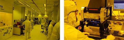
Figure 2.1 NanoLab NL cleanroom facility at MESA+ Institute for Nanotechnology (left) with mask aligner apparatus for UV lithography in operation (right).
Images courtesy: S. Schlautmann, University of Twente, 2011.
The reader is referred to Madou [1], and Cui [2], for further details of lithographic techniques. Direct-writing of a pattern onto a resist transfers a computer-aided design (CAD) into the resist on the mask blank, and subsequently the pattern is transferred by etch-through into the light-blocking material. The mask blank, therefore, must be UV transparent and in most cases a borosilicate plate with a chrome layer as an absorber is used [3, 4]. The mask-making process is also a lithographic process, however, due to its serial write strategy it is slow. This makes it too expensive for use in large-volume production.
The selection of masking procedures and the choice of materials and techniques will influence the accuracy of the final device’s geometry, and, therefore, the device performance. Low-cost masks also exist. These are processed by printing the CAD design onto an ink-jet transparency, which is subsequently transferred to a standard mask blank using a mask aligner or UV-light box. However, resolution and line width roughness are restricted by the resolution of the printer.
The CAD files are often generated in specially designed software tools that provide functions for drawing a mask layout, which can be converted by the pattern generator into a latent image in the resist on the mask blank.
Lithographic and more recent plasma etch methods are commonly used to remove material, leaving strips, lines, dots and other shapes on the substrate with well-defined profiles and dimensions in the individual device components. The resolution achievable in photolithography is restricted by the diffraction of light and therefore it is limited in its lateral dimensions. The degree of resolution of a lithographic process refers to the narrowest distance that can exist between two lines such that they can still be transferred as two separated lines (fully resolved lines).
Other fast and novel direct-write strategies for wafer production have been developed recently. Novel parallel electron or ion beam techniques allow features to be copied at increasing manufacturing speed by multiplication of the active write element. Unfortunately, none of these techniques are yet on the market and are so far only available in research [5]. Such methods will overcome the limitations of optical diffraction, so extending the application of top-down patterning processes far into the sub-micron domain.
An overview of novel nanolithographic techniques is given in Chapter 4. Laser stereolithography or non-lithographic direct shaping methods (micro-milling, laser ablation, 3D-printing) may be used as direct-write fabrication techniques for less demanding dimensions. These techniques are also very popular for the fabrication of microfeatures during prototyping in research and development, and for small volume or single piece production. We will discuss some examples in Chapter 3.
2.2 Thin Films
Silica and silicon nitride are classical thin film materials, functioning as dielectrics and capping materials in microelectronics. Metals such as copper, gold, platinum, titanium and chromium are another type of materials used to make thin films forming conducting, masking, sacrificial or adhesion layers. A comprehensive overview of processes for the deposition and selective etching of thin films can be found in many texts, e.g., Vossen [6].
The range of materials used in microfabrication is extensive. Besides these conventional materials, various polymers, oxides and III-V-based semiconductors as well as many hybrid materials have been investigated for the production of integrated systems [7–12]. Many new, thin film systems have been designed, based on novel instruments, which are capable of the controlled manipulation of nanoparticles or even atoms during their deposition. These materials have very advanced properties, but they can still be deposited by fairly simple techniques from solution. A range of standard deposition techniques for thin films will be discussed in the following two sections.
2.2.1 Wet Deposition Techniques
Deposition of a paint occurs by evaporation of the solvent from the suspension. In traditional wall coatings (i.e., paint) the thickness of the final coating and its uniformity are obviously not very critical parameters. However, in microfabrication they are. Despite this major difference, the principles of deposition which are used for dipping, spin- or spray-coating in patterning at the micro- and nanoscale remain the same. The film-forming compounds are dissolved in a solvent. When this is spread onto the handling platform (substrate, wafer) the solvent starts to evaporate and the film is formed. Photoresist, e.g., Microposit® S1813, may be deposited by spin-coating [1, 13, 14]. This process can be supported by a baking process usually called a soft-bake at a modest temperature around 90°C.
As mentioned previously in Section 2.1, a resist system may act either as a positive or a negative photoresist. In a positive resist, the area modified during the lithography step is removed from the substrate. This creates openings that allow to act on subsequent process steps. In negative resists, the lithographically-manipulated region remains on the substrate.
Besides masking, novel nanotechnology-based coating processes also allow the formation of more complex thin films by relatively simple deposition techniques which exploit such processes as polymer-demixing of multiphase systems (two or more phases are dissolved and remain in the matrix of the material) and may include nanoparticles (e.g., nanosphere lithography). When spreading the hybrid organic–inorganic nanocomposite suspension onto a substrate, e.g., by spin-coating, the building blocks in the material systems reorganize to minimize the energy state of the film. This can also explain why room temperature annealing over a period of a few hours enhances the ordering of such matrix systems after deposition of the film. Single layers of different properties may alternate during deposition, and form a so called layer-by-layer film by self-assembly, which may not only have the alternating original functions of each individual layer, but also completely new properties [15, 16]. An introduction to such novel techniques and special thin-film materials can be found in Chapter 4, Section 4.2.
2.2.2 Vapor Deposition Techniques
The reader is referred to references [17], [18] and [19] for further details on this topic, since this discussion is intended as an introduction.
Thermal evaporation of metals having low to moderate deposition rates (10–100 nm/min) is regarded as one of the traditional physical vapor deposition (PVD) techniques. It relies on the sublimation of material onto a substrate in a vacuum. In industrial applications, the so called sputtering process is often preferred to thermal evaporation, because of better step coverage, a wider choice of possible materials (includes dielectrics) and often higher deposition rates (up to a few 100 nm/min), while forming dense films with an appropriate adhesion quality. Sputtering forms ions from an inert gas, which are accelerated against a target material. This then goes into the plasma phase and deposits onto the substrate (the work piece) as a film. The process was developed to meet the requirements of large scale integration (LSI) in the 1970s and 1980s. Film properties are actively controlled by manipulating parameters like bias, pressure and substrate heat. These control mechanisms allow for higher reproducibility, a better device optimization and result in adapted material properties. Depending on the properties of the film-forming compounds, it is also possible to incorporate special properties, e.g., UV sensitivity into the film, specifically investigated for advanced lithography resist materials [20].
Chemical synthesis, using precursors in the gas phase at elevated temperatures is also possible. These are called chemical vapor deposition (CVD) techniques. The elevated temperatures that are necessary restrict its use to wafer materials that can withstand these deposition temperatures, and match to a certain extent the thermal expansion coefficient of the deposited film. If these processes are conducted at subatmospheric pressures they are called low pressure chemical vapor deposition (LPCVD). Nearly all CVD processes are carried out at low pressure, to avoid unwanted gas-phase reactions and improve film unformity at elevated reaction temperatures. If a plasma is used to provide energy during the material deposition process, it is called plasma-enhanced chemical vapor deposition (PECVD). These techniques are of interest in applications where a low substrate temperature and a high-density film is received. CVD techniques involving a plasma reactor are fully established in industrial production.
A variety of methods in which the plasma not only provides the energy source but also enables different modes of deposition are also available [21]. Parameters such as the total reactor pressure, frequency of the rf-excitation, rf-power and growth temperature all influence the film morphology. Although other film-forming processes exist, physical and chemical vapor deposition techniques are the ‘workhorses’ of industrial thin film applications. Figure 2.2 shows two such thin film generating apparatuses.

Figure 2.2 NanoLab NL cleanroom facility at MESA+ Institute for Nanotechnology. Top left: low pressure chemical vapor deposition (LPCVD) oven. Bottom left: loading a thermal evaporator. Right: showing the interior of the vacuum chamber of the evaporator with the wafer carousel on the top part of the figure and the crucible at the chamber bottom.
Images courtesy: S. Schlautmann, University of Twente, 2011.
Pulsed laser deposition (PLD) is a recent technological development, and an example of the shift in research to nanotechnology [22]. A new material can be composited based on an understanding of reaction kinetics in the gas phase.
This technique can be used to design thin films with unique properties, e.g., magnetic, superconductive, negative thermal and electrical resistance materials and multilayers. Thin films clearly possess the potential for innovative micro- and nanofabrication applications, and for deepening our understanding of their physicochemical properties at the nanoscale level. These can be investigated by scanning tunneling microscopy and other novel imaging techniques that resolve atomic interaction phenomena stirred by the deposition process. New thin film technologies also involve a search for novel materials. It is therefore very exciting for researchers and developers to discuss thin films in the broader context of the innovation stimulated by nanotechnology.
2.3 Silicon Micromachining
Silicon is one of the fundamental materials of the semiconductor industry and was used nearly exclusively in the early applications of microsystems technology (MST). Even now silicon is the preferred material for the initial testing and integration of devices because its patterning techniques are very well known. Silicon offers a high degree of monolithic integration capacity and has very good mechanical properties. It remains a very attractive material because of the high quality of wafer finishing achievable. This also makes it an interesting material for mechanical sensor applications, since they often rely on precise bonding at the wafer level [23–25].
The fact that silicon wafers are a relatively inexpensive commodity allows researchers in commercially yet less attractive fields access to this base material and to run a variety of well-defined processes. However, this can bias the choice of fabrication techniques, and researchers often look for a work-around in their device designs to meet silicon micromachining techniques. This approach sometimes precludes a successful (cost-efficient) implementation of a new technology. On the other hand, silicon is indispensible for making demonstrators of a novel functional mechanism at small scales although the material may be substituted for alternatives if the device goes into full-scale production. The controlled deposition of thin films and their partial removal by wet or dry etching play an important role in silicon micromachining.
Wet chemical etching is a fairly simple technique to perform, and the associated equipment costs are relatively low [26]. However, established silicon micromachining techniques are restricted to etching in layers up to a few micrometers in thickness, which are inadequate for some device criteria. The increasing demand for three-dimensional device structures has motivated many research groups to develop specific high aspect-ratio technologies with high precision [27–30]. Such techniques may include deep dry etching and three-dimensional masking in combination with anisotropic wet etching in silicon [31]. In reality, a microfabrication sequence can involve a great many processing steps to produce just one functional component of a system, e.g., microneedles or comb-like shaped actuators (comb-drives). Further details of the fabrication sequence for a range of devices and systems will be described in Chapter 5 (micromechanical transducers), Chapter 6 ((bio)chemical sensors), Chapter 7 (Lab-on-a-Chip systems) and Chapter 8 (microdevices for medical applications). The following sections of this chapter will review the variety of basic techniques for microfabrication specifically in silicon. The information is based on Petersen’s comprehensive introduction to silicon as a micromechanical material (1982) [25].
2.3.1 Etching
Wet Chemical Etching
Wet etching is a purely chemical approach for the removal of layers or bulk material, the following processes are recognized as standards.
Buffered oxide etch (BOE) contains NH4F/HF/H2O and is used for the etching of thermal oxide, LPCVD oxide and PECVD oxide, or low temperature oxides (LTO). BOE patterning can be performed using, for example, a positive resist (e.g., AZ1500 series from AZ Electronics Materials plc) with a defined thickness of 1.2, 1.8 or 6.5 μm [32]. Tetramethylammonium hydroxide (TMAH) or potassium hydroxide (KOH) silicon etchant is used for the crystal-oriented anisotropic etching of mono silicon. Thermal oxide or LPCVD nitride masks are commonly used for patterning.
A so-called HF-dip is used for etching thin silicon oxide (gate oxides, native oxide layers). A phosphoric acid (H3PO4) etch can be performed for uniform stripping of silicon nitride layers (LPCVD nitride, PECVD nitrides).
Aluminum etch is a special mixture of acids, used for etching of aluminum layers (e.g., interconnection lines). Polysilicon etch is a mixture of HF and HNO3 and is used for isotropic etching of polysilicon layers.
Many other reagents are used for special applications, including special etchants for metal layers (Au, Cr, Ni, Cu, Ti). Figure 2.3 depicts an example of a standard wet-etch bench (top left) including a special rinsing system, a quick-dump rinser (bottom left) and schematic representations of two types of etching mechanisms in silicon (right).

Figure 2.3 NanoLab NL cleanroom facility at MESA+ Institute for Nanotechnology. Chemical etch acid/solvent wet bench (top left) and wafer handling at the quick dump rinsing station (bottom left). Schematic wet etching profiles in silicon (right).
Image courtesy: S. Schlautmann, University of Twente, 2011.
The chemistry of the reactions is isotropic in nature, unless selective etch rates are established due to crystallographic planes or change in materials (e.g., using etch-stop layers). However, isotropic (wet) chemical etching frequently suffers from instability of the masking layer at the edge of a pattern, due to lateral under-etching. Thin, overhanging parts of the mask can break off, thereby increasing the line width roughness. Isotropic wet etching is therefore restricted in resolution, and produces rougher, thicker lines than dry processing. Anisotropic wet etching differences in etch rates of different crystallographic planes is far less sensitive to line width roughness, but it may still suffer from delamination of the masking layer. Current design tolerances, and also the hazards involved when working with and disposing of large amounts of hazardous liquid-based chemicals, make these processes less attractive for industrial production than dry etching in vacuum systems, despite their simplicity. A comprehensive overview of etch rates for micromachining processing is given by Williams and Muller [33].
Dry Etching
Many available dry-etch processes bombard the wafer with ions through a masking layer. Some of these techniques can etch extremely deep features with vertical side walls, which will be described in more detail in Chapter 3. Here, an introduction is given to this ever more important technique of microfabrication. Unlike directional wet etching, these processes do not rely on the orientation of the crystal structure (lattice) but the selectivity of the etch rates of the materials used as masking layer and work piece. Selectivity is particularly restricted if physical ion bombardment is the major mechanism of the etching process (e.g., ion milling).
Basically, these ion etching processes use a parallel plate configuration to make a plasma in an inert gas under reduced pressure. If specially shaped electrodes are used to confine the plasma, and reactive gas species are used, then the etch rate and selectivity can be enhanced and the etch profiles can be tuned. Figure 2.4 summarizes the events which occur in a conventional reactive ion etch (RIE) process, as described in a variety of microfabrication processing handbooks [34, 35].

The essential features of RIE are:
(b) anisotropy (preferential etching in a direction normal to the substrate surface), and
(c) selectivity (the etch rate ratio between the material to be removed and the masking material).
The RIE etch mechanism further includes:
(a) chemical etching for the creation of volatile products by reaction between the work piece material and the etch gas (e.g., fluorine-based gas) and
(b) sputtering, which refers to the interaction of ions with matter during the bombardment with chemically inert ions (e.g., Ar+) in the plasma.
Figure 2.5 depicts the schematic of a parallel plate etcher configuration and one example of an RIE-etched microstructure in silicon.
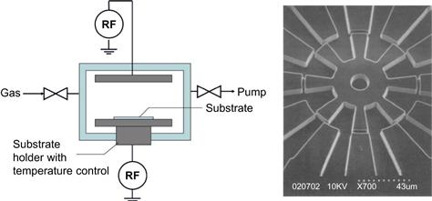
Figure 2.5 Schematic of a parallel plate plasma etching apparatus (left) and example of reactive ion etching result in silicon.
right, reproduced from reference [36].
2.3.2 Surface Micromachining
Various techniques have been developed to pattern different layers by surface micromachining. The principles of wet etching rely on the chemistry of dissolution of materials. Most of the processes are isotropic in nature and can be performed either in the liquid or the vapor phase. As mentioned in the previous section, dry processes are more complicated because they require a vacuum system and involve the generation of a plasma by electrical discharge, meaning that they need complex control equipment to modulate process parameters.
In dry etching processes, the use of a reactive gas species allows highly selective etching of the work piece in the presence of a masking layer. However, the specific gas chemistry, substrate temperature and field strength must be tuned to each material and etching application. In the case of plasma deposition processes, the gas mixture (i.e., composition) can be used to modify the layer properties of thin films. Patterning for many microelectromechanical devices has been demonstrated on thin films of polysilicon (PS). Micromotors with an electrostatic actuation principle were one of the early examples of successful polysilicon surface micromachining. This application of surface micromachining is introduced and illustrated in Figure 2.6. Figure 2.7 shows an etched and surface-released machined gear wheel that was fabricated using this processing sequence [37]. In general, fluorine-based plasma processing of silicon is selective against silica, which can be patterned either by RIE or in buffered HF. Other standard, dry etch, gas mixtures are chlorine- or bromine-based. Reference to a variety of process recipes can be found in various handbooks [34, 35].
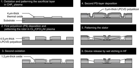
Figure 2.6 Integrated fabrication of a microgear-train realized from polysilicon.
Redrawn from reference [37].

Figure 2.7 Cross-sectional view of a typical structure resulting from the process sequence depicted in Figure 2.6, a gear-train with the largest gear of a radius of 120 μm.
Reproduced from reference [37] with permission
Surface micromachining utilizing polysilicon (PS) is a key technology or so-called standard microfabrication process, now used to manufacture an extensive variety of devices. Micromotors were made possible by surface micromachining techniques that define sacrificial layers by means of which a structural feature can be released from the substrate. This technique is also commonly applied in the design of resonant microdevices, as discussed in Chapter 5. Sacrificial silica processing can be also applied to smooth and clean surfaces, and to generally reduce the effects of friction for mechanical moving parts and in devices for media transport (e.g., microfluidic chips). Silicon surface micromachining is of less importance for integrated optical waveguides in the visible range, but it plays a key role for the integration of micro-opto-electromechanical systems (MOEMS) and other photonics devices which operate at longer wavelengths. In optical devices, the surface or side wall roughness is directly related to loss of reflectivity in mirror devices. This makes the definition of line edge and surface roughness crucial for optical applications. Of course, in the ever-increasing demand for electronic integration reducing line width roughness is also important in electronic devices.
Surface micromachining is a delicate process with a relatively low device yield. However, process optimization produced a commercially attractive manufacturing process in the early 1990s. A number of silicon manufacturing foundries were established, and introduced a service for silicon processing and MEMS manufacture on demand, including multi-user MEMS processes (MUMPs®, where different users share device space on one wafer). This sharing of space is made possible by designing the devices according to a design routine which is supplied by the manufacturing foundry as a standard and thus at a reasonable price. Some of the players who first offered these foundry services were Sandia National Laboratories and Bosch. MEMSCAP, a French leader in the MEMS service industry, provides both standard and custom products to their clients. The MUMPs® program has run since 1992, following previous success at Cronos, a JDS Uniphase division. MEMSCAP acquired Cronos in 2002 and now it runs MUMPs® as a polymer, metal and silicon-on-insulator (SOI) process in addition to their standard complementary-metal-oxide-semiconductor (CMOS)–MEMS line.
2.3.3 Silicon Bulk Micromachining
A wide spectrum of machining techniques has emerged for the patterning of bulk silicon: from more conventional wet etching to complex anisotropic dry etching and novel, focused energetic beam processes. Once a new processing instrument is designed novel techniques can be derived for its use. Techniques are developed, and their specific patterning capabilities are researched. Further development produces a technology for the manufacture of components and systems.
Originally, many components were simply miniaturized versions of designs existing at a larger scale, hence, to begin with, silicon micro- machining offered high precision but also dictated certain design criteria. A set of standard technological processes has evolved, around these design criteria as process modules or steps, which can be used interchangeably. The microfabrication expert will generally talk about a new process technology when a certain set of such modules are put in a new sequence to allow a novel geometrical structure to be manufactured – but the individual steps will have been known for sometime. An example of this is the development of technologies for the manufacture of microneedle arrays [31]. Considerable effort is currently devoted to developing industrially robust methods for manufacturing ever-smaller devices. As with processing at the macroscale, many process developments are related to the efficiency or yield of the process.
In current bulk microprocessing, the designs for a specific functional element may vary a lot from application to application, requiring specific tuning of the process parameters (substrate temperature, gas species, plasma energy, process pressure, rf-bias). Process selection and optimization is therefore based on the specific purpose of a device. This approach results from the fact that the same type of device can be made by different, patentable technologies resulting in unique properties during the device application.
As mentioned previously, patterning can be performed either by parallel or by serial processing. A mass-market approach using parallel, or batch fabrication is more desirable from a commercial perspective. For example, deep reactive ion etching has become very popular since the development of the “Bosch process” for silicon etching resulting in a high quality and fast etch rate [38]. These processes can now be bought-in from various suppliers (microsystems foundries), e.g., Silex (Sweden), LioniX (The Netherlands) or Tronics-MST (France). Foundries belong to the service industry and generally do not develop their own microdevice. Bosch etching and wet anisotropic chemical etching are the microfabrication techniques in most common use at present, and are introduced in the next two sections.
Anisotropic Wet Chemical Etching
Silicon has been exploited to an enormous extent as a micromechanical material. Simple shapes like V-grooves and cavities may be produced in silicon by selectively removing material from the substrate [1, 26, 39–42]. Although the concept of silicon etching has been described in the aforementioned sources, a short overview is presented here, concentrating on successful industrial applications, such as the etching of micromachined mass-spring systems for accelerometers, or the diaphragm-based pressure sensor.
To produce such systems an etch-resistant material (e.g., thermal oxide) is deposited or grown on the surface of the substrate, and patterned by photolithography and wet etching. As mentioned briefly above, there are many chemical etchants for silicon, but ethylenediamine perizine (EDP), or less toxic solutions like potassium hydroxide (KOH) and tetramethylammonium hydroxide (TMAH) are well established wet silicon bulk etchants.
Figure 2.8 depicts the type of vessel that is used for the process. The etchants in the double-walled vessels are temperature-controlled by a water bath recirculation system. Here, several 4″ wafers are vertically mounted in a special quartz-glass rig. Their arrangement allows several wafers to fit into the vessel, and allows the hydrogen gas that is evolved during the etching process to escape from the structures. Etchant selection depends on the application. Etch rates are approximately 1μm/min, and etch times of 2–3 hours are fairly normal in these processes.
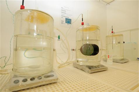
Figure 2.8 NanoLab NL cleanroom facility at MESA+ Institute for Nanotechnology. Examples of a typical vessel used in silicon bulk micromachining by KOH-etching.
Image courtesy: H.A.G.M. van Wolferen, University of Twente, 2011.
Timed etching, or etch stops such as a boron-doped silicon layer may be employed [43, 44]. The crystal-oriented etch characteristics of silicon in anisotropic etchants depends on the fact that the etch rate decreases dramatically when it reaches an inhibiting crystal plane [45–47]. Special simulation software has been developed to predict etch shapes. The high etch rates of so-called convex corners must be treated with particular care. An example of a silicon structure and its possible fabrication are shown in Figure 2.9 and Figure 2.10. More advanced information about the wet and dry etching of silicon is presented in an excellent review paper by Kovacs et al. [48].
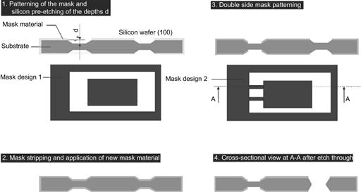
Figure 2.9 Process sequence for bulk etching with aligned double-side exposure.

Figure 2.10 Seismic mass of an acceleration sensor realized by silicon anisotropic wet etching.
Reproduced with permission from reference [49].
Bosch Process
Reactive ion etching by the Bosch processing technique utilizes an inductively coupled plasma (ICP) source and alternating gas chemistry for the controlled steps of reactive ion etching (RIE) and deposition. Such an alternating process provides selectivity between silicon and the photoresist of 100:1, or over 200:1 if oxide is used as a masking material. These high ratios are obtained by using a plasma source which generates a very high plasma density but at the same time allows a high control over the ion bombardment energy. The use of fluorine-containing etch gases such as SF6 (etching) and C4F8 (passivation), means that the Bosch process can coat the side walls, and also opens the bottom of the structure, by highly directional ion bombardment. Passivation and etching cycles are automatically switched every 5 to 15 s. Figure 2.11 shows microstructures etched by the Bosch process.

Figure 2.11 Typical example of a microstructure generated by the Bosch process.
Image courtesy: J. G. Bomer, University of Twente, 2004.
2.4 Industrially Established Non-Silicon Processing
Microsystems rely on shaping many materials into structural elements. During the last two to three decades many materials other than silicon have been used, either in surface micromachining, or as a thin film, or for components produced by bulk micromachining. Examples include piezoelectric single crystal quartz, photostructurable glass or plastics. A diverse range of materials has been investigated for use in this area. The following sub-sections illustrate basic fabrication principles that are often used in industrial applications.
2.4.1 Quartz Etching
Single crystal (SC) materials, such as single crystalline quartz, may be also patterned anisotropically in a similar way to silicon. Selective wet etching of specific crystal planes offers efficient removal rates using chemical etchants and can deliver high precision. SC-quartz wet etching has been widely investigated for the manufacture of frequency-control timebases as well as for a variety of sensors (force, strain, acceleration, temperature, pressure, to name a few). However, its application in fields other than tuning forks is rare. The complex crystal structure makes prediction of etch shapes more difficult than it is possible for silicon.
Quartz has been used as piezoelectrical material for micromechanical resonator devices. However, with respect to multifunctional capabilities quartz’ major advantage is its optical transparency and its use has not yet been fully exploited for sensing and actuation through use of the piezoelectric effect. Also, quartz wafers can be cut along a symmetry axis, as such that a tuning fork device may be aligned in such a way that the symmetric fork design can compensate for temperature effects in the resonant behaviour [50, 51].
Bulk micromachining quartz for a micro-optoelectromechanical system is described by Sugiyama et al. [52], and shown in Figure 2.12. Miniature resonant tuning forks are used in the wristwatch industry. The steps of a double-side process are shown in Figures 2.13 and 2.14 [53].
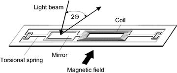
Figure 2.12 Quartz resonant scanner, electromagnetic scanning principle.
Redrawn from reference [52].
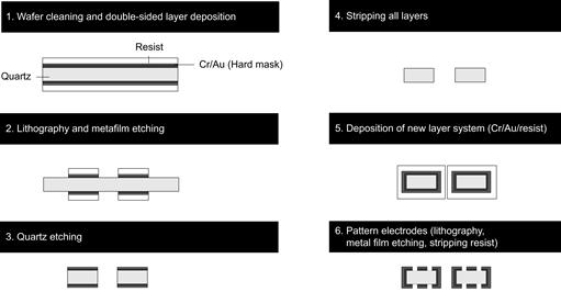
Figure 2.13 Process sequence for SC-quartz tuning forks.
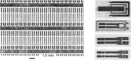
Figure 2.14 Left: quartz tuning fork resonators manufactured on a quartz wafer by photolithography. Right: various types of batch fabricated quartz resonators manufactured by the technique described above in Figure 2.13.
Reproduced from reference [53] with permission
2.4.2 Glass Wet Etching
Amorphous glasses, including fused silica, can be etched in a similar way to single-crystal quartz. Examples are the isotropic etching of borosilicate glass in hydrofluoric acid (HF), in which a strip-opening in the masking layer will result in a hemispherical channel structure if sufficient etch time is allowed. Figure 2.15 demonstrates the application of this technique to the fabrication of microfluidic channels [54].

Figure 2.15 Scanning electron micrograph of cleaved edge of microfluidic channel etched in glass by HF.
Reproduced from reference [54].
This process is very important for the fabrication of microfluidic-assisted biochips, which are a successful emerging market. Various chip manufacturers and high-tech suppliers, such as Philips and Agilent, have invested in Lab-on-a-Chip technology to develop their own applications in this field.
2.4.3 Photostructurable Glass
Amorphous glass is of great interest for the microfabrication of optical integrated microelectromechanical systems (MOEMS). It is possible to photochemically modify special glass by applying ultra-violet light [55]. This so-called photoetchable glass has been available for some time [1], and is now being used where structures with good thermal and electrical isolation are required. The resolution of the lateral dimension, however, is relatively low but high aspect ratios can be achieved. Pattern transfer characteristics are as follows: illumination of material up to 2 mm thickness; a convex feature with an aspect ratio of up to 40:1; the remaining surface roughness is in the order of 1 μm. Using Foturan® glass, various geometries can be realized, with the width of walls as low as 50 μm, the length of walls up to 100 mm and the diameter of holes (concave features) as low as 50 μm in substrates of 1 mm thickness. The material can be used in a similar way to a silicon or glass wafer, and has a surface finish quality appropriate for creating a bond at wafer level. Metal coatings can be applied for a variety of applications, too. One example of the application of photostructured glass is in the field of microreactors [56]. To pattern through 1 mm thick Foturan® plates a photo-energy density of 2 Joule/cm2 is required. Silver clusters are formed within the exposed areas. The second step requires a heat treatment between 500°C and 600°C. The thermal energy causes crystallization of the glass around the silver atoms.
These crystallized regions can be etched up to 20 times faster than conventional glass (e.g., BK 7) and unexposed Foturan® in a 10% hydrofluoric acid solution at room temperature. Foturan® is a trademark speciality glass manufactured by Schott AG, Mainz, Germany. PEG3 is another photosensitive glass synthesized by the Hoya Corporation, Tokyo, Japan, and although these types of glasses are important their commercial activity has been discontinued for PEG3 already some time ago. The principal steps of the processing technique are depicted in Figure 2.16. An anisotropic etch profile results due to the difference in solubility between the exposed and unexposed regions. An example of photoetched devices is displayed in Figure 2.17. Additional information concerning custom manufacturing in Foturan® can be found on the mikroglas chemtech GmbH website [57]. A new photostructurable glass, FS21, has also been developed at the Technical University Ilmenau, Germany.

Figure 2.16 Photostructurable glass process sequence.

Figure 2.17 Microfabricated titer plate made from Foturan®.
Image courtesy and original: mikroglaschemtech GmbH, Mainz, Germany [57].
2.4.4 Powder Blasting
A method from applications in the macro world adapted uses a stream of abrasive particles. Ceramic-based particles from alumina or silicon carbide are used. Micro-abrasive blasting is an efficient technique for the low-cost patterning of hard, brittle materials such as glass, silicon, tungsten and ceramics. The material is removed from the work piece (target) by the mechanical impact of accelerated particles as depicted in Figure 2.18.
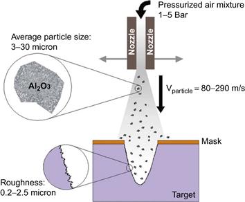
Figure 2.18 A schematic diagram of the powder blasting process.
Reproduced from reference [58] with permission from IOP Publishing.
An example of this erosion technique applied to Pyrex® glass is shown in Figure 2.19. This technology has been thoroughly investigated for application to microtechnology. Particles with an average size of 29 μm or 9 μm are used depending on the degree of allowed surface roughness. The smaller the particles are, the slower is the blasting process. The definition of process parameters, mask materials and restrictions of applications have been published amongst others in Wensink [59, 60]. Features in the order of tens of microns can be produced, and the technique has been used successfully for producing wafer vias and fluidic microchannels as well as for large-scale production in flat panel displays [61–63]. Although powder blasting is a serial process it is very interesting from the point of rapid prototyping and the manufacture of wafer through-holes in glass micromachining.

Figure 2.19 Typical result in Pyrex® using powder blasting. Channels are 400 μm deep.
Reproduced from reference [58] with permission from IOP Publishing.
2.4.5 Plastic Microfabrication
Plastics are a very special class of materials with a diverse range of properties. Unfortunately, the exact composition or chemical structure of the materials being developed in the polymer industry for microsystems device manufacture has not been specified. An exception to this is the development of polymers for photoresists and as packaging materials for electronics.
In brief, some specific characteristics of plastics materials are: light weight, low cost, large range of tunable optical properties including transparency, low thermal and electrical conductance, and favorable biocompatibility and permeability. A plastic product may also be a polymer blend or composite instead of a single polymer. Plastics suppliers may use different brand names, but are likely to deliver products (monomers, sheets and granulates) of equal quality. This variety in supplies may lead also to additional variables during the design and optimization of a microfabrication process. Within the microfabrication service industry this offers a business niche. A foundry service provider can guarantee that polymer base materials are bought in such large quantities that their properties are consistent, offering their customers one-stop shop solutions for machining and fabrication services, and a source of materials.
Many of the materials used in injection molding or hot embossing could also be used in microsystems. The specific properties of these thermoplastics have to be evaluated and optimized for specific microsystems applications. Thermosetting polymers, such as duroplasts and elastomers, are used more rarely. The silicon elastomer (PDMS) is now being used in micro- and nanofabrication processes by a special technology known as soft-lithography, which is a process that produces a soft (flexible) micro- or nanostructure generated from a hard master. The hard master is usually formed by photolithography.
For plastic micromolding, the number of possible materials is so vast that we will restrict the current discussion to some key polymers and the basic microfabrication techniques that are used. Micro-cutting, -milling and -drilling are also used for shaping polymers. Here, we will focus on four of the innovative polymer-forming techniques that were specifically developed for microfabrication purposes. More detail on these topics can be found in the literature [1, 2, 13, 64]. The examples presented here, are intended as a guideline to polymer microfabrication in the emerging microsystems’ market [65].
Thick Resist Lithography
We have already introduced the principle of photolithography for thin polymeric films. These techniques have been taken further through the development of an epoxy-type photoresist called SU-8, which allows single layer lithography up to a thickness of several hundred micrometers. This photoresist is very successful in MEMS because it can be done with an existing UV mask aligner equipment, either directly or with minimal adaptation. Being able to produce structures with such a thickness in standard cleanroom facilities created a kind of microfabrication revolution all around the world. Figure 2.20 presents a patterned layer of 200 μm thick SU-8 on a silicon wafer, illustrating the possibility of vertical profiles [66].

Figure 2.20 SU-8 thick photoresist lithography on silicon.
Reproduced from reference [66] with permission from IOP Publishing.
SU-8 overcame the barriers for patterning three-dimensional structures in mechanical and chemical stable resist. In the early 1990s this was only possible by the use of x-ray lithographic processes. This was difficult because of the need for expensive x-ray beam lines from synchrotron sources. X-ray lithography can be used for patterning structures that require extremely vertical side walls and significant height (very high aspect ratios). Therefore it is often known as a 2.5-dimensional approach in the MST community although complex, three-dimensional features such as photonic crystals or filters can also be generated [67]. The so-called LIGA concept – the German abbreviation of LIthographie (lithography), Galvanik (galvanoforming) and Abformung (molding) – made this process economically feasible. However, it also needed non-standard substrates and has now been replaced by SU-8 in most of the initial application areas. X-ray LIGA is now a niche market and remains as a speciality technique operated by the research groups and institutes that have direct access to a beam line facility. We will discuss LIGA in more detail in Chapter 3.
Realizing three-dimensional microstructures also allowed SU-8 lithography to be used for the fabrication of micromechanical devices (Chapter 5), and molds for galvanoforming and/or direct replication into a polymer (see the sub-section on polymer micromolding below). SU-8 lithography is also popular as a master for the fabrication of mold structures for specific soft-lithography techniques. If patterned SU-8 is used as a mold for galvanoforming processes, it is often referred to as UV-LIGA and can be applied to advanced microtechnologies in combination with replication processes in metal and ceramics. A functional SU-8 photoresist structure may be formed by multilevel UV exposure producing a variety of complex structures, e.g., components of a microgear system such as that depicted in Figure 2.21. The application of this type of microfabrication to miniature gears was successfully introduced to the market by the watch industry.

Laser Ablation
Accurate processing of complex three-dimensional microstructures can be performed by removal of material using excimer or Nd:YAG lasers as an energy source. The laser energy is absorbed at the surface of the work piece and disintegrates the material. Due to the pulsed nature of the process, the heat does not penetrate into the deeper layers of the work piece. Such processing, by superficial removal of material is called ablation. Excimers with wavelengths of 157, 193 and 248 nm are suitable for large area ablation, and Nd:YAG lasers are normally used for small-volume ablation since the latter allow for higher frequency pulses. Figure 2.22 illustrates a laser ablation process and its possibilities for an example of a plastic microstructure. The much longer wavelength of a CO2-laser may also be used, however, with a less defined pattern accuracy than excimer and Nd:YAG lasers. KrF excimer laser ablation etch rates for polymers such as polysulfone (PSU), polyetheretherketone (PEEK) and polyimide (PI) have been studied as a function of the laser fluence (ε). With increased fluence a higher pattern accuracy (inclination angle of the side wall) and reduced debris formation is observed. An overview of various aspects (materials, processes and applications) of the utilization of laser ablation in micro- and nanofabrication processes for polymers is presented by Dyer [69]. Masks may be utilized in excimer laser ablation. Efficiency is increased for complex structures by directly transmitting a large mask geometry in parallel into the polymer surface. The femtosecond laser micromachining principle and an example of a microfluidic channel produced in PMMA is detailed in Marco et al. [70], who specifically investigate the surface roughness of the ablated surface over different laser fluences.

Figure 2.22 Top left: Diagram showing femtosecond laser micromachining method. Right: (a) Scanning electron microscope (SEM) image of ablated microchannel produced in polymethylmetacrylate (PMMA); (b) ablated depth versus incident laser fluence. Experimental data points are well represented by a logarithmic (dashed line). The x-intercept of the fitted logarithmic reveals a threshold fluence of 0.85 J/cm2 (N = 20 pulses per spot).
Reproduced with permission from reference [70].
Photopolymerization
Local control of photopolymerization processes initiated by a suitable light source is also considered to be a rapid prototyping technique for complex three-dimensional (3D) polymer microstructures. Obviously price per piece should not be a specific concern when using this technique. However, if only a small number of devices are required, this technique is extremely valuable and effective. A three-dimensional CAD design can be directly translated, layer-by-layer, into the movement of a table containing a photosensitive resin. At the focal point of the laser, the resin gets exposed to such a degree that polymerization of the liquid monomer occurs. The use of a photosensitive polymer that solidifies during exposure has certain drawbacks for the direct manufacture of functional devices or components, specifically with respect to the mechanical strength and hardness of the material. Nevertheless, this process can be used to manufacture maskless polymeric mold structures for subsequent replication processes, either in polymer micromolding (see below) in lost mold replication processes, for example, ceramic microfabrication. The latter will be discussed in Chapter 3.
Microstereolithography is also possible for the direct fabrication of ceramic green-state structures from hybrid ceramic-filled polymer precursors. In Figure 2.23 (left) a schematic of the apparatus is depicted, and on the right of the figure are two types of products. For industrial processes, the current resolution is in the order of 100 μm, and depends on the mechanical accuracy of the elevator displacement of the stage which carries the work piece during the layer-by-layer building process. Currently, attempts are being made to reduce this resolution down to the nanoscale by a two-photon approach, in which two beams have to intersect to reach the energy threshold for polymerization. The technique can form 3D objects directly, with a lateral resolution that depends on the focusing spot of the laser beams, but can be as small as 120 nm [71]. UV lasers may also be used for the stereolithographic process, but only infrared (IR) lasers can be applied for the two-photon technique. Since this process is a point-by-point exposure process it is very slow, but it can be speeded up by irradiating the outer boundaries of a design. This process first produces a shell-type structure, which is subsequently solidified, irradiating by UV flood exposure of the enclosed monomer.
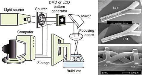
Figure 2.23 Left: schematic of a microsterolithography apparatus and typical result thereof. Top right: design studies for micromixers. (Reproduced by permission of The Royal Society of Chemistry [72].) Bottom right: three interwoven springs fabricated by stereolithography. (Figure left and bottom right reproduced from reference [73].)
Thermoplastic Micromolding
In these micromolding processes, thermoplastic polymers are heated somewhat above their glass transition temperature (Tg). Tg is a characteristic of a given polymer, and one can roughly say that polymers with higher molecular weight also have a higher Tg. Polymethylmetacrylate (PMMA), for example, has a Tg of 150°C, which is a modest process temperature. This allows cycle times of a few minutes to be used for molding by hot embossing. The term nanoimprinting is preferred for the thermally induced re-shaping of a polymer at the nanoscale, which we will further discuss in Chapter 4.
Many different techniques have been demonstrated in the literature, but only a few, such as the fabrication of metal molds by micro-milling or a combination of either x-ray or SU-8 lithography and galvanoforming have to date found their way into industrial-scale MST applications. The machines used for micromolding have also been specially developed. Jenoptik Mikrotechnik, Jena, Germany, for example, originally developed the HEX for applications in micro hot-embossing. Other players also have successfully entered the market using the same thermal polymer printing process at the nanoscale, known as thermal nanoimprinting (see Chapter 4, Section 4.1.6).
Figure 2.24 shows a schematic of a micro hot-embosser, a hot-embossing chamber and resultant microfabricated devices. The examples were supplied by the Microfluidic ChipShop, Jena, Germany, who offer microfabrication foundry services, including micromolding processes.
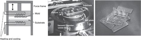
Figure 2.24 Left: schematic drawing of micro hot-embossing equipment. (Reproduced from reference [74].) Middle: close-up of a polymer substrate inside the vacuum chamber of a hot-embossing machine. Right: micromolded plastic microfluidic chips for the mixing of pharmaceuticals. (Reproduced from reference [75].)
The mold manufacturing process for micro hot-embossing may be carried out by combining of thick resist lithography (x-ray resist or SU-8) and galvanoforming. Alternatively, it is possible to use micro-cutting, laser ablation, silicon micromachining or other plastic-forming processes (e.g., photolithography) for the construction of a production mold. The mold can be fabricated from one piece, or assembled from different pieces constructed to various accuracy and step height constraints to create the complete mold insert (see, for example, Figure 2.21, Section 2.4.5 above). There are few indicators as to which of the techniques is better with respect to a given application challenge. However, metal molds are good temperature conductors, and they are very robust.
Silicon, although mechanically a tough material, is brittle and tends to chip or crack during these harsh applications. For the so-called soft-lithographic molding processes this type of limiting factor is of less concern and these silicon is therefore often used in prototyping and research. Stamps are usually made from nickel, but polymers may also be used to reduce the cost per stamp. However, this type of soft mold can deform when temperatures of several 100°C and high pressure is applied during the mold-filling sequence. The fabrication of micro vias for printed circuit boards (PCB), for example, can be performed by the imprint technique and is demonstrated in Figure 2.25. The stamp is pressed into a silica reinforced epoxy resin [77].

Figure 2.25 Printed circuit board (PCB) micro via patterning by thermal imprint technology.
Reproduced from reference [76].
Besides hot embossing (often now called imprinting for realizing patterns at the nanoscale) injection micromolding is often used when up-scaling to a high-volume production is required. The cycle time, in the order of seconds for injection molding, is the most important parameter in large-scale production. Figure 2.26 depicts a schematic drawing of an extruder feeding the mold tool within an injection apparatus. The lower panel of the figure shows a micro-pump fabricated in the biocompatible polymer Topas® by thinXXS GmbH, Zweibröcken, Germany. Microparts for microfluidic operations are a leading example for the successful introduction of science-based technologies into the market.

Figure 2.26 Top: schematic drawing of an injection molding equipment. (Reproduced from reference [78], Copyright © 2000 John Wiley & Sons, Inc.) Bottom: thinXXS presents a micropump injection molded in Topas®. (Original source: thinXXS, accessed online [79].)
Attia et al. have compiled a comprehensive overview of the available literature on microfabrication processes and machines with a dedicated focus on microfluidics structures [77].
2.5 Conclusions
This chapter has provided the reader with an overview of basic microfabrication techniques. It has covered photolithography and thin-film technologies, adopted from the microelectronic industry, the development of thick resists and other novel material shaping processes. These techniques have lead the way to new applications of microfabrication processes for, e.g., microfluidic devices.
Silicon is an excellent mechanical material and is utilized in diaphragms or special resonant sensors and micro-optical systems involving special comb-type and mass-spring type structures, often requiring high aspect ratio features directionally etched into the bulk of the silicon wafer. The cubic crystallography of silicon offers designers an accurate but relatively simple and low-cost process for achieving a diversity of such microstructures.
Wet chemical etching of other single-crystal materials are also explored for special purpose applications, such as single-crystal quartz in timebase devices.
In many current design processes, plasma-based dry etching is a preferred technology although this choice may be based more on access to equipment than application needs. Surface micromachining for freely moving mechanical structures in silicon has been also developed for their integration with the electronics circuitry on the same platform (silicon wafer). Such monolithic integrated devices are offered as a multi-user process by foundries in the microfabrication service industry.
MST foundry services are increasing in popularity, and more and more academic facilities are opening their doors to industry, not only for research but also for production.
In conclusion, the basic techniques described here reflect the standard processes available nowadays in the microsystems technology industry. The field remains a very dynamic market place, and the continuous development of novel materials will lead to further extension of the microfabrication tool box, some examples of which will be given in the following chapters.
REFERENCES
1. Madou MJ, ed. Fundamentals of Microfabrication. New York: CRC Press; 1997.
2. Cui Z. Micro- Nanofabrication Berlin: Springer; 2005.
3. Glendinning WB, Helbert JN, eds. Handbook of VLSI Microlithography. Park Ridge, NJ, USA: NOYES Publications; 1991.
4. Chang CY, Sze SM, eds. ULSI Technology. New York: McGraw-Hill; 1996.
5. Kruit P, Mohammadi Gheidari A. Multi-electron beam systems. In: Wakaya F, Inoue Y, Moon JH, eds. Technical Digest of the 22nd International Vacuum Nanoelectronics Conference. 2009;89–90.
6. Vossen JL, Kern W. Thin Film Processes II New York: Academic Press; 1991.
7. Martin P, Skouri EM, Chusseau L, Alibert C, Bissessur H. Accurate refractive index measurements of doped and undoped InP by grating coupling technique. Appl Phys Lett. 1995;67:881–883.
8. Seassal C, Leclercq JL, Viktorovitch PJ. Fabrication of InP-based freestanding micro-structures by selective surface micromachining. J Micromech Microeng. 1996;6:261–265.
9. Garrigues M, Leclercq JL, Viktorovitch P. III-V semiconductor based MOEMS devices for optical telecommunications. Microelectron Eng. 2002;61–62:933–945.
10. Dreyer C, Bauer M, Baue J, Keil NJ, Yao H, Zawadzki C. Polycyanurate ester resins with low loss for use in integrated optics. First International IEEE Conference on Polymers and Adhesives in Microelectronics and Photonics 2001;276–283.
11. Yeatman EM, Ahmad MM, McCarthy O, et al. Optical gain in Er-doped SiO-TiO waveguides fabricated by the sol-gel technique. Opt Commun. 1999;164(1–3):19–25.
12. Wörhof K, Driessen A, Lambeck PV, Hilderink LTH, Linders PWC, Popma ThJA. Plasma enhanced chemical vapor deposition silicon oxynitride optimized for application in integrated optics. Sens Actuators. 1999;A 74(1–3):9–12.
13. Rai-Choudhury P. Handbook of Microlithography, Micromachining, & Microfabrication. vol. 1 Washington, USA: SPIE Optical Engineering Press; 1997.
14. Shipley Europe Ltd, Microposit® S1813 photo resist. Technical report, Shipley Europe Ltd, Shipley House, Herald Way, Coventry, CV3 2RQ, UK.
15. Han TH, Ok T, Kim J, et al. Bionanosphere lithography via hierarchical peptide self-assembly of aromatic triphenylalanine. Small. 2010;6(8):945–951.
16. Decher G. Fuzzy nanoassemblies: toward layered polymeric multicomposites. Science. 1997;277(5330):1232–1237.
17. Pliskin WA. Comparison of properties of dielectic films deposited by various methods. J Vac Sci Technol. 1977;14(5):1064–1081.
18. Kern W. Advances in deposition processes for passivation films. J Vac Sci Technol. 1977;14(5):1082–1099.
19. Rojas S, Modelli A, Wu WS, Borghesi A, Pivac B. Properties of silicon dioxide films prepared by low-pressure chemical vapor deposition from tetraethylorthosilicate. J Vac Sci Technol. 1990;B 8(6):1177–1184.
20. Nault M, Weidman T, Sugiarto D, Mui D, Lee C, Yang J. Single layer chemical vapor deposition photoresist for 193 nm deep ultraviolet photolithography. J Vac Sci Technol B: Microelectron Nanometer Struct. 1998;16(6):3730–3733.
21. Cote DR, Nguyen SV, Stamper AK, et al. Plasma-assisted chemical vapor deposition of dielectric thin films for ULSI semiconductor circuits. IBM J Res Dev. 1999;43:5–38.
22. Blank DHA, Koster G, Rijnders GAJHM, Van Setten E, Slycke P, Rogalla H. Epitaxial growth of oxides with pulsed laser interval deposition. J Cryst Growth. 2000;211(1):98–105.
23. Buser RA, de Rooij NF. Very high Q-factor resonators in monocrystalline silicon. Sens Actuators. 1990;A 21–23:323–327.
24. Chui BW, Stowe TD, Ju YS, et al. Low-stiffness silicon cantilevers with integrated heaters and piezoresistive sensors for high-density AFM thermomechanical data storage. J Microelectromech Syst. 1998;7(1):69–78.
25. Petersen KE. Silicon as a mechanical material. Proc IEEE. 1982;70:420–458.
26. Wolf S, Tauber RN. Silicon Processing for the VLSI Era: Process Technology. vol. 1 Sunset Beach, CA, USA: Lattice Press; 1986.
27. Cheng Y, Lin C-Y, Wei D-H, Loechel B, Gruetzner G. Wall profile of thick photoresist generated via contact printing. IEEE J Microelectromech Syst. 1999;8.
28. Bischofberger R, Zimmermann H, Staufert G. Low-cost HARMST process. Sens Actuators. 1997;A 61:392–399.
29. Fischer K, Klein J, Chaudhuri B, Guckel H. Design and fabrication of one millimeter high structures. Microsystem Technol. 1998;4(4):176–179.
30. Kufner M, Kufner S. Fabrication of monolithic integrated fiber-lens connector arrays by deep proton irradiation. Microsystem Technol. 1996;2:114–118.
31. Gardeniers HJGE, Luttge R, Berenschot EJW, et al. Silicon micromachined hollow microneedles for transdermal liquid transport. IEEE J Microelectromech Syst. 2003;12(6):855–862.
32. Microchemicals. http://www.microchemicals.com/, (accessed 04/04/11).
33. Williams KR, Muller RS. Etch rates for micromachining processing. J Microelectromech Syst. 1996;5(4):256–269.
34. Glocker DA, Shah SI. Handbook of Thin Film Process Technology. vol. 1 London, UK: IOP Publishing Ltd; 1995.
35. Rossnagel SM, Cuoma JJ, Westwood WD, eds. Handbook of Plasma Processing Technology. Park Ridge, NJ, USA: Noyes Publications/William Andrew Publishing LLC; 1990.
36. Legtenberg R, Jansen H, de Boer M, Elwenspoek M. Anisotropic reactive ion etching of silicon using SF6/O2/CHF3 gas mixtures. J Electrochem Soc. 1995;142(6):2020–2028.
37. Mehregany M, Gabriel KJ, Trimmer WSN. Integrated fabrication of polysilicon mechanisms. IEEE Trans Electron Devices. 1988;35(6):719–723.
38. Dijkstra P, Schilp K, Hausner M. Can SEA (semiconductor equipment assessment) also deliver for MEMS?. VIDE. 2001;56(302):684.
39. Schwartz B, Robbin H. Chemical etching of silicon, part I. J Electrochem Soc. 1959;106(6):505–508.
40. Schwartz B, Robbin H. Chemical etching of silicon, part II. J Electrochem Soc. 1960;107(2):108–111.
41. Schwartz B, Robbin H. Chemical etching of silicon, part III. J Electrochem Soc. 1961;108(4):365–372.
42. Schröpfer G, de Labachelerie M, Tellier CR. Application and simulation of unconventional bulk-micromachining using underetching of 100 silicon planes. Microsystem Technol. 1999;5:194–199.
43. Seidel H, Csepregi L, Heuberger A, et al. Anisotropic etching of crystalline silicon in alkaline-solutions 1 Orientation dependence and behavior of passivation layers. J Electrochem Soc. 1990;137(11):3612–3626.
44. Seidel H, Csepregi L, Heuberger A, et al. Anisotropic etching of crystalline silicon in alkaline-solutions 1 Influence of dopants. J Electrochem Soc. 1990;137(11):3626–3632.
45. Bean KE. Anisotropic etching of silicon. IEEE Trans Electron Devices. 1978;25(10):1185–1193.
46. Koide A, Sato K, Tanaka S. Simulation of two-dimensional etch profile of silicon during orientation-dependent anisotropic etching. In: Micro Electro Mechanical Systems, 1991, MEMS ‘91, Proceedings An Investigation of Micro Structures, Sensors, Actuators, Machines and Robots. 1991;216–220.
47. Lee S, Park S, Cho D-I. A new micromachining technique with (111) silicon. Jpn J Appl Phys. 1999;38:2699–2703.
48. Kovacs GTA, Maluf NI, Petersen KE. Bulk micromachining of silicon. In: Proceedings of the IEEE, Special Issue Integrated Sensors, Microactuators & Microsystems (MEMS). 1998;1536–1551.
49. Geßner T, Vetter E, Wiemer M. Technology tools for a high precision accelerometer in bulk micromechanics. Microsystem Technol. 1994;1(1):10–13.
50. Hornsteiner J, Born E, Fischerauer G, Riha E. Surface acoustic wave sensors for high-temperature applications. In: Proceedings of the Annual IEEE International Frequency Control Symposium. 1998;615–620.
51. Clayton LD, Eernisse EP, Ward RW, Wiggins RB. Miniature crystalline quartz electromechanical structures. Sens Actuators. 1989;20(1–2):171–177.
52. Sugiyama N, Yamazaki D, Ueda T. A quartz galvanometer for optical scanning in a laser printer application. International Conference on Solid-State Sensors and Actuators, 1991 Digest of Technical Papers, TRANSDUCERS ’91 1991;734–737.
53. Momosaki E. A brief review of progress in quartz tuning fork resonators. Proc IEEE Int Freq Control Symp. 1997;552–565.
54. Koutny LB, Schmalzing D, Taylor TA, Fuchs M. Microchip electrophoretic immunoassay for serum cortisol. Anal Chem. 1996;68(1):18–22.
55. Dietrich TR, Ehrfeld W, Lacher M, Krämer M, Speit B. Fabrication technologies for microsystems utilizing photoetchable glass. Microelectron Eng. 1996;30(1–4):497–504.
56. Yunus K, Marks CB, Fisher AC, et al. Hydrodynamic voltammetry in microreactors: Multiphase flow. Electrochem Commun. 2002;4(7):579–583.
57. Mikroglas Chemtech GmbH, www.mikroglas.com, (accessed 04.04.11).
58. Wensink H, Jansen HV, Berenschot JW, Elwenspoek MC. Mask materials for powder blasting. J Micromech Microeng. 2000;10(2):175–180.
59. Wensink H, Berenschot JW, Jansen HV, Elwenspoek MC. High resolution powder blast micromachining. In: Proceedings 13th International Workshop on Micro Electro Mechanical Systems (MEMS 2000). 2000;769–774.
60. H. Wensink, Fabrication of microstructures by powder blasting, PhD thesis, University of Twente, Enschede, The Netherlands, ISBN 90-365-1698-6, 2002.
61. Solignac D, Sayah A, Constantin S, Freitag R, Gijs MAM. Powder blasting as a novel technique for the realisation of capillary electrophoresis chips. Proc Eurosensors. 2000;XIV:345–346.
62. Schlautmann S, Wensink H, Schasfoort R, Elwenspoek M, van den Berg A. Powder-blasting technology as an alternative tool for microfabrication of capillary electrophoresis chips with integrated conductivity sensors. J Micromech Microeng. 2001;11(4):386–389.
63. Ligthart HJ, Slikkerveer PJ, in’t Veld FH, Swinkels PHW, Zonneveld MH. Glass and glass machining in ZEUS panels. Philips J Res. 1996;50:475–499.
64. Franssila S. In: Introduction to Microfabrication. Hoboken, NJ, USA: Wiley; 2010.
65. Becker H, Gärtner C. Polymer microfabrication technologies for microfluidic systems. Anal Bioanal Chem. 2008;390(1):89–111.
66. Lorenz H, Despont M, Fahrni N, LaBianca N, Renaud P, Vettiger P. SU-8: A low-cost negative resist for MEMS. J Micromech Microeng. 1997;7(3):121–124.
67. Feiertag G, Ehrfeld W, Freimuth H, et al. Fabrication of photonic crystals by deep x-ray lithography. Appl Phys Lett. 1997;71(11):1441–1443.
68. Bertsch A, Lorenz H, Renaud P. 3D microfabrication by combining microstereolithography and thick resist UV lithography. Sens Actuators A Phys. 1999;73(1–2):14–23.
69. Dyer PE. Excimer laser polymer ablation: Twenty years on. Appl Phys A: Mater Sci Process. 2003;77(2):167–173.
70. Marco CD, Eaton SM, Suriano R, et al. Surface properties of femtosecond laser ablated PMMA. ACS Appl Mater Interfaces. 2010;2(8):2377–2384.
71. Tanaka T, Sun H-B, Kawata S. Rapid sub-diffraction-limit laser micro/nanoprocessing in a threshold material system. Appl Phys Lett. 2002;80(2):312.
72. Bertsch A, Heimgartner S, Cousseau P, Renaud P. Static micromixers based on large-scale industrial mixer geometry. Lab Chip Minituarization Chem Biol. 2001;1(1):56–60.
73. Bertsch A, Bernhard P, Vogt C, Renaud P. Rapid prototyping of small size objects. Rapid Prototyping J. 2000;6(4):259–266.
74. Becker H, Heim U. Hot embossing as a method for the fabrication of polymer high aspect ratio structures. Sens Actuators A Phys. 2000;83(1):130–135.
75. Bertsch A, Bernhard P, Vogt C, Renaud P. Rapid prototyping of small size objects. Rapid Prototyping J. 2000;6(4):259–266.
76. Ra S, Lee C, Cho J, et al. Micro via and line patterning for PCB using imprint technique. Curr Appl Phys. 2008;8(6):675–678.
77. Attia UM, Marson S, Alcock JR. Micro-injection moulding of polymer microfluidic devices. Microfluid Nanofluidics. 2009;7(1):1–28.
78. Becker H, Gärtner C. Polymer microfabrication methods for microfluidic analytical applications. Electrophor. 2000;21(1):12–26.
79. www.thinxxs.com.