2
Design of an Accelerated Squarer Architecture Based on Yavadunam Sutra for Machine Learning
A.V. Ananthalakshmi*, P. Divyaparameswari and P. Kanimozhi
Department of ECE, Puducherry Technological University, Puducherry, India
Abstract
A novel acceleration strategy of a squarer architecture is proposed for machine learning so as to reduce the hardware complexity and thereby achieve superior performance. Complex mathematical operation can be greatly simplified by adopting Vedic mathematics. Efficient arithmetic operations are required to carry out real-time applications. Multipliers are frequently employed in signal processing. Hence multipliers can be designed using a squarer unit. Squaring Circuit offers a very good performance in terms of speed. Thus squaring module becomes the fundamental operation in any arithmetic unit. The squaring operation is frequently employed in cryptography also. On the whole, squaring operation is widely encountered in multipliers. While designing multipliers, it is essential to reduce the hardware complexity with less power consumption. Vedic mathematics simplifies the design concepts and thus paves the way for high-speed applications. On comparing the various Vedic sutras, Yavadunam sutra is highly efficient from logic utilization and is found to be suitable for high-speed digital applications. Hence, a squaring architecture has been designed using Yavadunam sutra, an ancient sutra of Vedic mathematics without using a multiplier circuit. The proposed acceleration strategy employs only addition operations. The design is simulated and realized using Xilinx Isim Simulator.
Keywords: Squarer circuit, Vedic multiplier, Yavadunam sutra
2.1 Introduction
Recently, deep learning algorithms gained popularity in contrast to the classical method. In mobile and edge devices, for classifying Histogram of Oriented Gradients (HOG) feature extractor is mainly used in Support Vector Machine (SVM) classifier, so as to achieve remarkable performance and thereby try to bring down the hardware complexity. One should achieve this by reducing the computational complexity without compromising on accuracy. Area and power reduction plays a crucial role in VLSI system design. High-speed adders and multipliers are essential in the design of a high-performance system. To meet the demand in high-speed applications, the design of high-speed multipliers increases the hardware complexity as well as the power consumption. To overcome the above said drawback, Vedic mathematics finds its extensive use in the design of hardware arithmetic units. Thus this work employs Vedic mathematics in the design of a squarer so as to achieve superior performance with reduced complexity.
The essential idea behind the Histogram of Object oriented Gradients Descriptor (HOD) is that the object appearance and shape of an image is identified using the intensity of gradient and edge direction. The gradient is computed using the following expression:
In order to compute the gradient, squaring operation is required. This work focuses on the implementation of high-performance squarer architecture by reducing the complexity without compromising on accuracy.
Several works were reported in the literature on the design of a squarer architecture. Vedic mathematics uses simple techniques and hence can be applied in the implementation of any mathematical operation [1]. An n-bit squarer using Vedic multipliers was proposed in [2] in which generation of partial products and its summation were done simultaneously to speed up the process. However, this has increased the hardware complexity. High-speed binary squaring architecture was proposed in [3, 4] which was based on Urdhva Tiryagbhyam Sutra (UTS) technique. This work also offers good performance at the cost of logic density. The squarer circuit based on peasant multiplication technique was introduced in [5] but this design has also increased the area. Vedic mathematics is applied in the design of a binary squarer and cube architecture so as to minimize the power dissipation [6]. Yavadunam algorithm finds its use in the squarer architecture as it produces good performance [7]. Nikhilam Sutra rules [8] were employed in the design of a squaring unit. This architecture has improved the speed but at the cost of area. An 8-bit and a 16-bit squarer circuit was proposed in [9] based on Antyayordashakepi Sutra and duplex technique. Both the designs offered good performance but at the cost of logic density. In [10] an efficient squarer was proposed based on Yavadunam algorithm for high-speed digital applications. All previously reported works had designed a 2-bit squaring circuits using which higher order bit multipliers were designed [11, 12]. In any hardware implementation, delay, area and power consumption becomes the primary concern. High-speed arithmetic systems heavily depend on high-speed adders and multipliers which in turn depend on squarer circuits [13–15]. [16–18] presents the high-speed multiplier architectures. From the literature survey it is inferred that an n-bit squaring circuit based on a Vedic multiplier requires more logic gates and thus results in more area. As Yavadunam sutra is highly efficient for high-speed digital applications, this work focuses on the design of a 4-bit squarer using a 3-bit squarer by employing Yavadunam sutra [19]. Design of an accelerated HOD/SVM for object recognition is proposed in [20] by reducing the computational operations just by using the addition operation. Hardware accelerator for machine learning was proposed in [21] with an aim to reduce the computational complexity. A power efficient hardware accelerator using FPGA was proposed in [22]. The hardware implementation of UCB algorithm was proposed in [23].
2.2 Methods and Methodology
Though Yavadunam sutra has been considered as the powerful squaring algorithms there is no efficient hardware architecture. Thus to begin with, an n-bit squaring circuit using Yavadunam sutra is designed where n = 4. However, it has resulted in more logic utilization. Hence a n-bit squaring circuit is designed using an (n-1)-bit squaring circuit so as to achieve higher speed. However, the design of an n-bit squaring circuit based on (n-1)-bit squaring circuit not only achieves higher speed but has also consumed less gates than an n-bit multiplier and thus resulted in less logic area. The objective of this work is to design an n-bit squarer using an (n-1)-bit squarer and thereby to reduce the i. The main goal is to implement a squaring circuit that does not rely on an area-consuming multiplier.
2.2.1 Design of an n-Bit Squaring Circuit Based on (n-1)-Bit Squaring Circuit Architecture
In the design of an n-bit squaring circuit based on (n-1)-bit squaring circuit where ‘n’ = 4, the numbers from 0 to 15 are considered. By keeping 8[1000] as the centre value, the numbers are divided into three cases as shown in Figure 2.1. The numbers below 8[1000] are treated as a single case, A < B. The numbers greater than 8[1000] are considered as the second case, i.e., A > B. In the third case, the centre value A = B is taken into account.
From Figure 2.1,
A ![]() Four bit input,
Four bit input,
B ![]() Base (deficiency) of input, i.e., base value B = 1000 since the input is a 4-bit data.
Base (deficiency) of input, i.e., base value B = 1000 since the input is a 4-bit data.
2.2.1.1 Architecture for Case 1: A < B
Figure 2.2 shows the block diagram of an n-bit squaring circuit based on (n-1)-bit squaring circuit for case 1, i.e., A < B where ‘n’ = 4. A 4-bit input that must be squared meets the condition of being less than 8[1000]. ‘D’ represents A[(n-2) down to zero] where ‘n’ = 4. As a result, 4 – 2 = 2, and we must consider from 0th to 2nd bit of the input. The value of ‘D’ is sent to the 3-bit squaring circuit, which performs squaring operations and outputs as 6-bit labeled ‘M’. As we are squaring 4-bit numbers, we need 8-bit output, so two zeros are placed before the value of ‘M’ and labeled as ‘X’, where ‘X’ is the squared output of ‘A’.

Figure 2.1 Block diagram for n-bit squaring circuit based on (n-1)-bit squaring circuit.

Figure 2.2 Block diagram for n-bit squaring circuit based on (n-1)-bit squaring circuit for case 1: a < b.
2.2.1.1.1 (n-1) – Bit Squaring Architecture
(n-1)-bit squaring circuit is used in the design of an n-bit squarer circuit where ‘n’ = 4. Table 2.1 presents the truth table for (n-1)-bit squaring circuit. The (n-1)-bit squaring circuit has been designed only using the basic logic gates as represented in Figure 2.3.
Table 2.1 Truth table for (n-1) – bit squaring circuit.
| N(3) | N(2) | N(1) | S(6) | S(5) | S(4) | S(3) | S(2) | S(1) |
|---|---|---|---|---|---|---|---|---|
| 0 | 0 | 0 | 0 | 0 | 0 | 0 | 0 | 0 |
| 0 | 0 | 1 | 0 | 0 | 0 | 0 | 0 | 1 |
| 0 | 1 | 0 | 0 | 0 | 0 | 1 | 0 | 0 |
| 0 | 1 | 1 | 0 | 0 | 1 | 0 | 0 | 1 |
| 1 | 0 | 0 | 0 | 1 | 0 | 0 | 0 | 0 |
| 1 | 0 | 1 | 0 | 1 | 1 | 0 | 0 | 1 |
| 1 | 1 | 0 | 1 | 0 | 0 | 1 | 0 | 0 |
| 1 | 1 | 1 | 1 | 1 | 0 | 0 | 0 | 1 |

Figure 2.3 Architecture for 3 – bit squaring circuit.
2.2.1.2 Architecture for Case 2: A > B
Figure 2.4 presents the block diagram for n-bit squaring circuit based on (n-1)-bit squaring circuit for case 2 where A > B with the assumption ‘n’ = 4. The input block receives the 4-bit number that we want to square. The input (A) is sent to a block called 2’s complement, which inverts the 4-bit input and then adds one, yielding ‘E’ as the output. As the input to the A < B block meets the first case’s criteria, the steps taken in case 1 are repeated here, and the result is labeled as ‘M’. The input ‘A’ is left shifted 4 times since ‘n’ = 4. As a result, the input is shifted left by four times, and the output is labeled as ‘I’. One of two 8-bit ripple carry adder is used to combine the ‘M’ and ‘I’ outputs, which are labeled as ‘H’. Another is used to combine the ‘H’ and ‘I’ outputs into a single ‘Z’ output. To obtain an 8-bit output, the first eight bits of ‘Z’ are treated as the squared output of a 4-bit input (A).
Thus if A > B, then the squarer operation is implemented using adder, subtractor and shift elements alone.
2.2.1.3 Architecture for Case 3: A = B
Figure 2.5 presents the block diagram for n-bit squaring circuit based on (n-1)-bit squaring circuit case 3, i.e., A = B. In this case, the centre value 8[1000] is used to calculate the squared output of 8 as 64. Simply shift the input, i.e., 8[1000], left three times to obtain the required output.
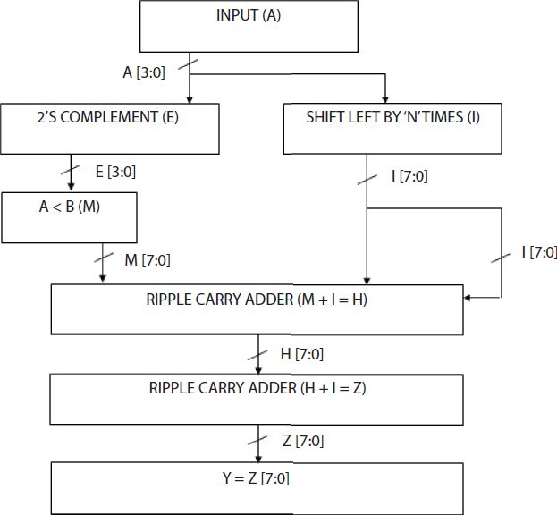
Figure 2.4 Block diagram for n-bit squaring circuit based on (n-1)-bit squaring circuit for a > b.
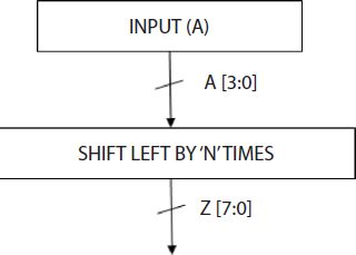
Figure 2.5 Block diagram for n-bit squaring circuit based on (n-1)-bit squaring circuit for a = b.
In Figure 2.5, if A = B, then the squarer operation is implemented using left shift operation.
2.3 Results and Discussion
In a 4-bit squaring circuit based on Vedic multiplier, a 2-bit multiplier is required which consists of a half adder whose simulated output is illustrated as shown in Figure 2.6. The binary inputs are 1 and 0 and the outputs are 1 and 0, respectively.
The full adder functionality is shown in Figure 2.7. The inputs are 1, 1, 0 and the outputs are 0 and 1 respectively.
The functional verification of a 4-bit ripple carry adder is shown in Figure 2.8. The inputs are 0001, 0000 and 1 and the 4-bit sum is 0010 and carry is 0.
The functional verification of a 2-bit multiplier is shown in Figure 2.9 where ‘a’ and ‘b’ are inputs and produces output as ‘p’. The values of input ‘a’ and ‘b’ are 2 and 3 and produces output ‘p’ as 6, respectively.

Figure 2.6 Half adder output.

Figure 2.7 Full adder output.
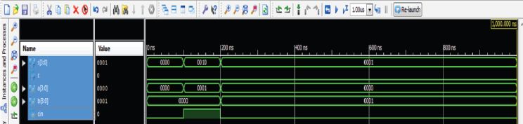
Figure 2.8 4-bit ripple carry adder output.
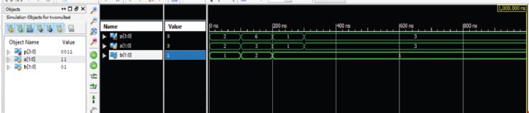
Figure 2.9 2-bit multiplier output.
A 4-bit multiplier is needed in a 4-bit squaring circuit based on Vedic multiplier, whose output is shown below in Figure 2.10. The inputs to 4-bit multiplier are ‘a’ and ‘b’ and produces ‘p’ as output. The inputs ‘a’ and ‘b’ are 5 and 5 and produce the value of ‘p’ as 25, respectively.
The output of an n-bit squaring circuit where ‘n’ = 4 based on Vedic multiplier is shown in Figure 2.11. The input is 15 and the squared output is 225.
The simulation result of an (n-1)-bit squaring circuit where ‘n’ = 4 is shown in Figure 2.12. The input is 3 and the squared output is 9.

Figure 2.10 4-bit Vedic multiplier output.

Figure 2.11 n-bit squaring circuit based on Vedic multiplier output where ‘n’ = 4.
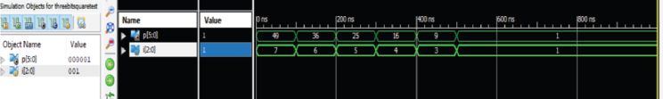
Figure 2.12 (n-1)-bit squaring circuit output where ‘n’ = 3.
The simulation output of an n-bit squaring circuit based on a (n-1)-bit squaring circuit is shown in Figure 2.13, where ‘a’ is the input to be squared and ‘p’ is the squared output of ‘a’. Figure 2.13 shows that the input value of ‘a’ is 15 and produces 225 as the squared output of ‘a’ respectively.
Table 2.2 presents a comparison between an n-bit squaring circuit based on Vedic multiplier and an n-bit squaring circuit based on (n-1)-bit squaring circuit, where delay, area and logic utilization are compared. The logic utilization of an n-bit squaring circuit based on an (n-1)-bit squaring circuit is reduced by 18% where as the delay is retained.
Table 2.3 compares the number of gates used in an n-bit squaring circuit based on Vedic multiplier and an n-bit squaring circuit based on a (n-1)-bit squaring circuit. From the results, it is inferred that logic complexity of the latter is approximately half of that in the former.
As the number of transistors used determines the size of an integrated circuit, the number of transistors required in an n-bit squaring circuit based on Vedic mathematics will be definitely more when compared to an n-bit squaring circuit based on an (n-1)-bit squaring circuit as the logic gates required is more in the former when compared to the latter.
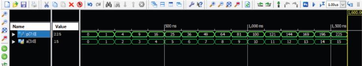
Figure 2.13 n-bit squaring circuit based on (n-1)-bit squaring circuit output where ‘n’ = 4.
Table 2.2 Comparison between squaring circuit based on Vedic multiplier and squaring circuit based on 3-bit squaring circuit.
| Performance parameters | Squaring circuit based on Vedic multiplier | Squaring circuit based on 3-bit squaring circuit |
|---|---|---|
| Power | 0.019W | 0.018W |
| Delay | 5.537ns | 5.537ns |
| Logic Utilization | 9 (56%) | 6 (38%) |
Table 2.3 Logic utilization for squaring circuit based on Vedic multiplier and squaring circuit based on 3-bit squaring circuit.
| Logic utilization | Squaring circuit based on Vedic multiplier | Squaring circuit based on 3-bit squaring circuit |
|---|---|---|
| 4 – Bit RCA | 3 | - |
| 8 – Bit RCA | 1 | 3 |
| Full Adder | 30 | 16 |
| Half Adder | 4 | - |
| Full Subractor | 1 | - |
| And Gate | 80 | 36 |
| Or Gate | 29 | 17 |
| XOR Gate | 64 | 33 |
| Not Gate | 16 | 2 |
| 2 Bit Multiplier | 4 | - |
| 3 Bit Squaring Circuit | - | 1 |
2.4 Conclusion
The performance of any VLSI implementation heavily depends on power, area and speed. For more accuracy and to simplify the hardware implementation one can apply Vedic mathematics. The n-bit squaring circuit based on Vedic multiplier has the disadvantage of requiring more logic gates and thus occupying more space with a greater number of logic elements. The n-bit squaring circuit design, which is based on a (n-1)-bit squaring circuit has fewer logic gates, takes up less space, and employs fewer transistors, resulting in the reduction in the size of the integrated circuit. When compared to a multiplier-based squaring circuit, this results in a 66% reduction in logic utilization, thus reducing the hardware complexity.
References
- 1. Fatemah K, Al-Assfor.; Israa S, Al-Furati.; Abdulmuttalib T, Rashid.; Vedic-Based Squarers with High Performance. Indonesian Journal of Electrical Engineering and Informatics (IJEEI) 2021, 9, 1, 163-172.
- 2. Kasliwal P. S.; Patil, P; Gautam D, K.; Performance evaluation of squaring operation by vedic mathematics. IETE Journal of Research 2011, 57, 1, 39–41.
- 3. Sethi, K.; Panda, R.; An improved squaring circuit for binary numbers. International Journal of Advanced Computer Science and Applications 2012, 3, 2, 111–116.
- 4. Kumar, A.; Kumar, D.; Hardware implementation of 16 * 16 bit multiplier and square using Vedic mathematics. International Conference on Signal, Image and Video Processing (ICSIVP) 2012, 309-314.
- 5. Kumar G. G.; Sudhakar C. V.; Babu M.N.; Design of high speed Vedic square by using Vedic multiplication techniques. International Journal of Scientific & Engineering Research 2013, 4, 1, 1–4.
- 6. Ramanammma, P.; Low power square and cube architectures using Vedic Sutras. International Journal of Engineering Research and General Science 2017, 5, 3, 241–248.
- 7. Deepa, A.; Marimuthu C, N.; High speed VLSI architecture for squaring binary numbers using Yavadunam Sutra and bit reduction technique. International Journal of Applied Engineering Research 2018, 13, 6, 4471–4474.
- 8. Nithyashree, S.; Chandu, Y.; Design of an efficient vedic binary squaring circuit. 3rd IEEE International Conference on Recent Trends in Electronics, Information and Communication Technology, RTEICT 2018 - Proceedings, 2018, 362–366.
- 9. Barve, S.; Raveendran, S.; Korde, C.; Panigrahi, T.; Nithin Kumar Y, B.; Vasantha M, H.; FPGA implementation of square and cube architecture using vedic mathematics. Proceedings - 2018 IEEE 4th International Symposium on Smart Electronic Systems, ISES, 2018, 6–10.
- 10. Deepa, A.; Marimuthu C, N.; VLSI Design of a Squaring Architecture Based on Yavadunam Sutra of Vedic Mathematics. Proceedings of the International Conference on Electronics and Sustainable Communication Systems (ICESC) 2020, 1162–1167.
- 11. Akhter, S.; Chaturvedi, S.; Khan, S.; A distinctive approach for vedic-based squaring circuit. International Conference on Signal Process. Integrated Networks, Spain 2020, 2, 27–30.
- 12. Koyada, B.; Meghana, N.; Jaleel M. O.; Jeripotula P. R.; A comparative study on adders. Proceedings of the 2017 International Conference on Wireless Communications, Signal Processing and Networking, WiSPNET, 2018, 2206–2230.
- 13. Kandula B. S.; Kalluru P. V.; Inty S, P.; Design of area efficient VLSI architecture for carry select adder using logic optimization technique. Computational Intelligence 2020, 1–11.
- 14. Kumar N. U.; Sindhuri K. B.; Teja K. D.; Satish D. S.; Implementation and comparison of VLSI architectures of 16-bit carry select adder using Brent Kung adder. Innovations in Power and Advanced Computing Technologies, I-PACT, 2017, 1–7.
- 15. Yaswanth, D.; Nagaraj, S.; Vijeth R. V.; Design and analysis of high speed and low area vedic multiplier using carry select adder. International Conference on Emerging Trends in Information Technology and Engineering, ICETITE, 2020, 8–12.
- 16. Deepa, A.; Marimuthu C. N.; VLSI Design of a Squaring Architecture Based on Yavadunam Sutra of Vedic Mathematics. International Conference on Electronics and Sustainable Communications Systems, 2020.
- 17. Deepa, A; Marimuthu C. N.; Murugesan; An Efficient High Speed Squaring and Multiplier Architecture using Yavadunam Sutra and Bit Reduction Technique. Journal of Physics Conference Series, 2020, 1432, 012080.
- 18. Deepa, A.; Marimuthu C. N.; Design of high speed Vedic Square and Multiplier Architecture Using Yavadunam Sutra. Sadhana Indian Academy of Sciences, 2019, 44, 9, 97, 1-10.
- 19. Deepa, A.; Marimuthu C. N.; High Speed VLSI Architecture for Squaring Binary Numbers Using Yavadunam Sutra and Bit Reduction Technique. International Journal of Applied Engineering Research, 2018, 13, 6, 4471-4474.
- 20. Shi, Lilong; Wang, Chunji; Wang, Yibing; Oh Kim, Kwang; Accelerated HOG + SVM for Object Recognition. Electronic Imaging Intelligent Robotics and Industrial Applications using Computer Vision, 2021, 317-1-317-3, DOI: https://doi.org/10.2352/ISSN.2470-1173.2021.6.IRIACV-317.
- 21. Li, Du; Yuan, Du; Hardware Accelerator for Machine Learning. Machine Learning 2017, DOI: 10.5772/intechopen.72845.
- 22. JiUn, Hong; Saad, Arslan; TaeGeon, Lee; HyungWon, Kim; Design of power - efficient training accelerator for convolution neural networks, Electronics, 2017, 10, 7, 787, https://doi.org/10.3390/electronics10070787.
- 23. Nevena, Radovic; Milena, Zogovic; Hardware Implementation of the Upper Confidence-bound Algorithm for Reinforcement Learning, Computers and Electrical Engineering, 2021, 96.
Note
- * Corresponding author: [email protected]