5
A Detailed Roadmap from Conventional-MOSFET to Nanowire-MOSFET
P. Kiran Kumar1,2*, B. Balaji1, M. Suman1, P. Syam Sundar1, E. Padmaja2 and K. Girija Sravani1
1 Department of ECE, Koneru Lakshmaiah Educational Foundation (Deemed to be University), Guntur, Andhra Pradesh, India
2 Department of ECE, Balaji Institute of Technology, Narasampet, Warangal, India
Abstract
Recently, the need for low-power, high-speed portable devices grew rapidly in the semiconductor industry. The developments in process technology made development of transistors with reduced dimensions, which led to the growth of the number of transistors on ICs. Also, the scaling of transistors along with CMOS technology made continuous upgrading of speed and power consumption of ICs. The scaled down transistor in the sub-100nm regime causes Short Channel Effects (SCE) such as lowering barrier height by drain supply, gate leakage, higher sub-threshold conduction and poly depletion, etc., and the effects of these are reduced by usage of various engineering techniques like metal work function, channel-doping profile and gate oxide. In the sub-45nm regime, the controllability on the channel is enhanced by introducing a new structure Thin-body SOI MOSFET with single and double gate. At 22nm nanometer technology, another new structure Fin-FET is proposed for further enhancement of controllability of gate on the channel. The Fin-FET utilizes double-gate, tri-gate, pi-gate, and omega-gate structures for further improvement of controllability. Further scaling down of MOSFETs to sub-10nm, the GAA nanowire-MOSFET exhibits better SCE immunity as compared to Fin-FETs. In this survey, we discuss the challenges in conventional MOSFET, advantages and limitations of Thin-body SOI-MOSFET, Fin-FET and various approaches to design nanowire-MOSFET in the sub-5nm regime. It is observed that the nanowire-MOSFETs have lower leakage and higher drive current as compared to other MOSFET structures at sub-5nm regime.
Keywords: Short-channel-effects, scaling challenges, thin-body SOI-MOSFET, Fin-FET, nanowire-MOSFET
5.1 Introduction
Silicon-based micro-electronic devices have changed human life in the last several decades and continue to have an extraordinary impact on all aspects of life today [1–3]. Such electronic devices and systems are used in a variety of applications including telecommunications, warfare, defense, medical, energy conservation, industrial automation, transportation, autonomous vehicles, amusement, infotainment, and the digital society [2–4]. The revolutionary changes in micro-electronics were experienced after fabrication of bipolar-junction-transistors [5, 6] and they further increased after the development of the first working ICs [7, 8]. Further, the development of MOSFET device and fabrication of amplifier with MOSFET allowed for integration of huge number of transistors along with connections on a single semiconductor wafer at lower cost [9, 10] and this led to the formulation of complementary-MOS (CMOS) device structure with pMOS and nMOS transistor for two-input and one-output inverter configuration [11]. In 1965, Gordon Moore predicted that the number of devices placed on a wafer would double every two years, and this prediction later became known as “Moore’s law” [12]. Moore’s rule was based on the premise that smaller devices enhance practically every element of IC functioning, especially lower cost and switching power consumption per transistor, as well as increased speed and memory capacity.
The growing need for battery-powered portable devices necessitated the development of electronic equipment that were operated with higher operating speed, lower power consumption, and were tiny in size. Each successive generation of IC technology has resulted in cheaper cost, higher device density, reduction in power consumption, and enhancement in processing speed IC-chips by scaling down device footprints according to scaling principles [13]. As per the scaling rule of MOSFET [13], as length of the channel (Lg) is reduced, then the oxide thickness is correspondingly reduced to maintain the same capacitive coupling between the gate terminal and inversion channel in relation to the other transistor terminals. As the scaling process is continued, the Short-Channel-Effects (SCEs) such as subthreshold swing (SS) deterioration, Hot Carrier Effects, Velocity saturation, threshold voltage (Vth) roll-off, and Drain-Induced Barrier Lowering (DIBL) are enabled, and the influence of these SCEs is severe when channel length is scaled down to beyond 100nm [14, 15]. In addition, along with the reduction in Lg there is a corresponding increment in the body doping (Nb) and a decrement in the source-drain junction depth Xj to reduce the subsurface leak path under the channel inversion layer. At each new technological node, the worldwide effort to miniaturize MOSFETs and circuit optimization in CMOS technology continues to produce ICs with higher computational speed, lower-power consumption, and lower cost [16, 17].
The US Semiconductor Industry Association (SIA) created the National Technology Roadmap for Semiconductors (NTRS) in 1994 and transitioned to the International Technology Roadmap for Semiconductors (ITRS) in 2000 by including global semiconductor companies in order to continue Moore’s law device miniaturization. Following Moore’s law and Dennard’s scaling rule, the ITRS set extensive criteria for future generations of technology. For multiple generations of VLSI technology, this scaling process has proven to be quite effective. However, due to insurmountable obstacles, standard MOSFET scaling methods could no longer provide positive advances in device performance established by Moore’s law for 100 nm planar-CMOS technology and beyond [14, 15]. In this paper we have discussed a couple of engineering techniques that have been developed to minimize SCEs in shorter length channels. The engineering techniques fall into classifications like Channel Engineering, Gate Oxide Engineering and Device Engineering, etc.
The remainder of the paper is organized in the following manner. The hardships experienced by Bulk-MOSFETs due to scaling of channel length are discussed in Section 5.2. Section 5.3 discusses the alternative concepts for conventional-MOSFETs. Section 5.4 examines the Thin-Body SOI-MOSFETS’s advantages and disadvantages with single and double gate over Bulk-MOSFETs. Section 5.5 demonstrates the non-planar structure of Fin-FET, advantages as well as its limitations. Section 5.6 focuses on another non-planar architecture of nanowire-MOSFET and various engineering techniques used to enhance its performance. The conclusion of this paper is discussed in Section 5.7.
5.2 Scaling Challenges Beyond 100nm Node
The worsening of leakage current is the most significant limitation to MOSFET device scaling in the sub-100 nanometer regime. The performance of MOSFET devices becomes increasingly reliant on gate length when they are scaled down to the nanoscale regime [18, 19]. As per the scaling rule, the bulk doping concentration is enhanced to prevent source-drain punch-through and subsurface leakage current when Lg is decreased. Because of the increased vertical electric field caused by enhancement in bulk doping concentration resulted in decrement in the mobility of the carrier and deterioration of the drive current in scaled devices. In addition to that, the increment in the band-to-band tunneling caused by high vertical electric field resulted in increment in the leakage current. Consequently, reduction in the gate length of MOSFET in the nanometer regime deteriorates the MOSFET characteristics, subthreshold slope and also lowers the threshold voltage (Vth) results Vth roll-off [20].
As demonstrated in Figure 5.1, regulating the leakage current in scaled devices is a critical challenge for continuous scaling of traditional bulk-MOSFETs. The noticed leakage current in downsized devices at nanoscale nodes is predominantly caused by leakage channels many nano-meters underneath the silicon/gate-dielectric contact [19]. To continue scaling of MOSFETs at the nanoscale node, tremendous efforts on channel engineering, shallow source-drain extensions (SSDE), and halo implants surrounding SSDEs [21–26] were made. However, for regular MOSFET structures beyond the 45 nm regime, the subsurface leakage current is unable to control by reducing gate-oxide thickness to as small as possible [19] and it led to development of new structures.
According to Roy et al. [14], there is considerable leakage current in deep-sub micrometer regimes as gate oxide thickness and gate length are lowered. When the gate length is lowered, SCEs such as weak inversion, Drain-Induced-Barrier-Lowering (DIBL), Gate-Induced-Drain-Leakage (GIDL), hot carrier injection, and gate oxide tunneling become sources of leakage currents. At the nanoscale node planar-MOSFET technology, there is a possibility of two ways for overcoming the scaling limits described above in traditional MOSFETs. The first approach is to incorporate new techniques, materials and doping methods into traditional planar MOSFETs in order to enable further reduction of device dimensions and performance improvement in scaled devices [27, 28]. Alternative device topologies, such as ultrathin-body MOSFETs and multiple-gate MOSFETs, provide greater electrostatic control over the inverted channel intrinsically [1, 19], as detailed in the next sections.

Figure 5.1 Drain current (Ids) versus gate voltage (Vgs) characteristics of the conventional n-MOSFET [19].
5.3 Alternate Concepts in MOFSETs
During the past two decades efforts have been made in research and development to explore alternate device topologies [1, 19, 29–34] for VLSI fabrication technology at nanoscale nodes in order to solve the rising hurdles in continuous reduction of device dimensions in traditional planar MOSFET devices. As illustrated in Figure 5.2 [35], Fujita et al. presented improved channel engineering to construct nanoscale MOSFET devices with un-doped/lightly-doped channels to reduce the influence of Random-Discrete-Doping. Conventional CMOS processing techniques are used to construct the channel on an intrinsic epitaxial-layer which is formed on a silicon substrate [35]. This type of MOSFET construction is called as Deeply-depleted-channel (DDC) MOSFETs [35]. The advantage of DDC device is decrement in Channel-Drain coupling capacitance due to highly doped channel layers 2 & 3 resulting in reduction of subsurface leakage current, and the process variability is controlled with the un-doped/lightly-doped channel [35]. The structure of the device is shown in Figure 5.2.
Figure 5.2 Deeply-depleted-channel MOSFET: In the schematic, region 1 is the undoped channel.
Figure 5.3 Buried-halo MOSFET device [37].
Further, Saha et al. designed halo doping around Source-Drain of the MOSFET to decrease subsurface OFF-state current. The halo doping refers to combining a lightly doped channel with highly doped implant. This double halo MOSFETs consisting of two halo doping profiles decreases the OFF-state current with the proper adjustment of threshold voltage in nano-meter devices [1, 24–26]. This device architecture is also called as “buriedhalo MOSFET (BH-MOSFET)”. In the fabrication of BH-MOSFET, halo doping profiles are implanted in the silicon substrate for the adjustment of threshold voltage. These processing steps are performed before the formation of the channel layer by epitaxy method. After epitaxy layer formation source drain regions as well as gate patterning is done [36, 37], which is illustrated in Figure 5.3. In comparison to traditional MOSFET devices, from the data available on threshold voltage variability, it is under-stood that there is a considerable decrement in threshold voltage variation because of Random-Discrete-Doping in nanometer BH-MOSFETs [1, 37].
5.4 Thin-Body Field-Effect Transistors
An alternative device structure used to reduce major OFF-state leakage current in the Silicon-On-Insulator MOSFET [38–40] and these are also called as Thin-Body MOSFETs. This device uses thin-body silicon as the channel, and it is the unique feature in the architecture of the device that ensures higher gate control of the channel for MOSFET devices. Placing of Ultrathin-silicon as the body on SOI-substrate and controlling of Ultrathin-silicon body using multiple gates [19] in different directions are the two techniques used to improve the controllability of the gate and decrease the drain controllability on the channel and Drain-Channel coupling capacitance.
5.4.1 Single-Gate Ultrathin-Body Field-Effect Transistor
As seen in Figures 5.4 and 5.5, the SOI devices are classified into two types, taking the silicon film thickness (tSi) into consideration. If the tSi is greater than the depletion width around Source/Drain then area of the channel is partially depleted, and this type of SOI device structure is referred to as a Partially Depleted (PD) SOI device. The region of the channel which is below the inversion layer is totally depleted when tSi is lesser than the depletion width, resulting in a Fully Depleted (FD) SOI device. The use of an ultrathin SOI substrate is to put silicon closer to the gate [41] and this can considerably reduce SCEs in MOSFETs. However, the device parameters such as thickness of silicon film, gate-oxide thickness, and doping concentration of body controls the SCEs in SOI substrate MOSFETs. From the literature, it is observed that the OFF-state current reduces when thickness of silicon film decreases [42, 43]. SCEs can be greatly reduced by lowering thickness of silicon film to roughly 7 to 14 nm, and it leads to end of leakage paths at buried oxide layer in SOI MOSFETs as shown in Figure 5.6 [42, 43]. The greater mobility in SOI MOSFET transistors leads to a large increase in ON-state current over a typical traditional MOSFETs [44]. SOI MOSFETs have lower parasitic junction capacitances, which accelerates the ON-state current and allows them to be faster than their bulk silicon MOSFETs [44]. There are two parasitic components, bulk capacitance and drain-channel coupling capacitance in traditional bulk-MOSFETs whereas SOI MOSFET contains only drain-channel coupling capacitance because of end of leakage lines at buried oxide layer which lead to decrement of parasitic capacitance in SOI MOSFET as compared to bulk-MOSFET.
Figure 5.4 Fully depleted (FD) SOI-MOSFET.
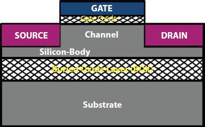
Figure 5.5 Partially depleted (PD) SOI-MOSFET.
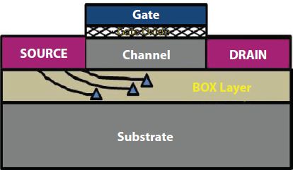
Figure 5.6 Ultrathin-body SOI-MOSFETs with termination of leakage paths in buried-oxide.
Furthermore, SOI MOSFETs are low-power devices due to their reduced inverse subthreshold, which allows for the usage of devices with lower threshold voltages without an increase in leakage current as compared to bulk-MOSFET devices with lengthy gate lengths [45]. This significantly minimizes static power usage. Additionally, using Ultrathin-Body MOSFETs on an intrinsic or weakly doped substrate lowers variability. UTB-SOI-MOSFETs have emerged as one of the most promising devices for advanced VLSI circuits at the nanoscale node [42, 43, 47–49].
Although SOI devices have numerous advantages, they also have certain reliability difficulties, such as self-heating due to insufficient heat dissipation [44]; thin film also causes hot-electron degradation [44], and floating-body effect in PD-SOI devices [44]. Thin SOI multi-gate MOSFET devices are particularly appealing beyond 32nm technology because of their outstanding electrostatic control and increased transport capabilities [46].
5.4.2 Multiple-Gate Ultrathin-Body Field-Effect Transistor
Usage of multiple gates around the channel or on the sides of the channel improves the controllability of the channel which leads to effective deterioration of SCEs; this is often called as multi-gate MOSFET devices. Figure 5.7 shows one type of multi-gate MOSFET with two gates placed at top and bottom of thin silicon body. For the Double-gate MOSFET structure illustrated in Figure 5.7, the sub-surface leaky lines far away from the top gate are nearer to the bottom gate and these are removed by the bottom gate which are caused by the top gate. Similarly, the subsurface leaky lines far away from the top gate are nearer to the bottom gate and these are removed by the bottom gate which are caused by the top gate. As a result, the gates top and bottom of the silicon body provide excellent controllability of the electrostatic inverted channel in a Doublegate-MOSFET, and it leads to reduction of SCEs. Therefore, the multi-gate MOSFETs scalability range is more as compared to planar bulk-MOSFET devices [50, 51].
In contrast to the conventional scaling principle, thin-body MOSFET structure which is shown in Figure 5.7 eliminates the need for high doping of the channel for deteriorating SCEs. The tuning of threshold voltage can done by adjusting channel doping concentration instead of adjustment of metal-gate workfunction [1, 18]. Further, the usage of less doping or intrinsic as channel in thin-body MOSFET decreases the random discrete doping in multi-gate MOSFETs and thus eliminates device performance fluctuation. Furthermore, less doping or intrinsic body reduces the channel average electric field, resulting in increased carrier mobility, lower OFF-state currents, and improved reliability of the device. This could help with the enhancement in the stability of bias temperature and deterioration of leakage tunneling current at gate-oxide [18].
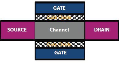
Figure 5.7 Ultrathin-body double-gate MOSFET.
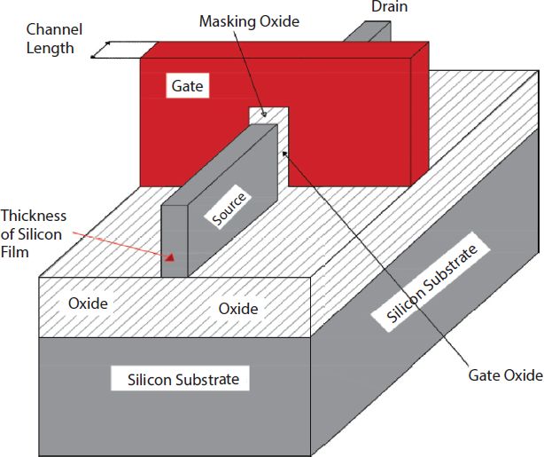
Figure 5.8 3-D ultrathin-body double-gate Fin-FET on silicon-on-insulator substrate.
Based on the foregoing, a thin-body double-gate MOSFET architecture, as illustrated in Figure 5.7, has a lot of potential for controlling SCEs and reducing OFF-state current as well as process variability by placing the gate near to the silicon body. Further, the rotation of double-gate MOSFET structure with 90 degrees forms a vertical double-gate MOSFET and it looks like placing MOSFET on silicon-substrate or SOI-substrate. The above said vertical double-gate MOSFET with thin fin-like body construction is called as FinFET as illustrated in Figure 5.8 and discussed in detail in the next section.
5.5 Fin-FET Devices
In terms of fabrication, among many MOSFET structures, Fin-FET architecture is the most viable multi-gate structure MOSFET. When compared to a conventional MOSFET device, this multi-gate thin-body device architecture has a higher resistance to SCE [1, 18]. In Fin-FET, the silicon sidewalls of the channel are controlled by the gate and it can be observed from three-dimensional Double-Gate FinFET architectures which are shown in Figures 5.8 and 5.9. The number of gates can be constructed along the sidewalls of the fin to increase the controllability of the channel in Fin-FET, and the number can be two, three or four. As the number of gates increases, fabrication complexity increases but higher electrostatic controllability of the channel can be achieved. Fin-FETs can be constructed on SOI-substrate as depicted in Figure 5.8 or on silicon-substrate as depicted in Figure 5.9. To construct Double-gate Fin-FET, the gate-dielectric is developed on either sides of the fin and dense masking-oxide is developed on fin-channel top, as can be observed from Figures 5.8 and 5.9. In the context of Triple-gate Fin-FET, the gate-dielectric is developed on either side of fin-channel as well as on the top of the fin-channel as shown in Figure 5.10. Therefore, the same thickness is used for either side of fin-channel and on the top of the fin-channel in triple-gate Fin-FETs.
In the subthreshold region, source-drain coupling is deteriorated in multi-gate Fin-FET, as the numerous gates constructed over the channel provide enhanced electrostatic control in the channel [52, 53]. The foremost thing is, an intrinsic channel is used in multi-gate FET which reduces the significant threat in process variability. Secondly, compared to conventional MOSFET devices fabricated using 32 nm planar-CMOS technology, multi-gate MOSFETs offer lower OFF-state current by an order of four. Thus in the manufacturing of advanced nanoscale devices multi-gate FETs are used in VLSI technology [52–54].

Figure 5.9 3-D ultrathin-body double-gate Fin-FET on bulk-silicon substrate.
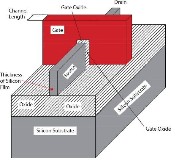
Figure 5.10 3-D ultrathin-body triple-gate Fin-FET on silicon-on-insulator substrate.
For sub-22 nm node VLSI circuits, FINFET is the industry-standard CMOS technology [52, 54–56]. To produce tolerable SCEs in FinFETs, the length of the gate should be around three times the thickness of the fin-channel [57]. The threshold voltage in FinFET is reduced by keeping leakage current constant due to improvement in the performance of short-channel and it results in enhancement of drive current by higher overdrive gate-voltage. At 22nm and 14nm nodes, the subthreshold swing was 70mV/decade and 65mV/decade, respectively [52, 55]. The ON-State current per device can be enhanced by increasing height of the fins and decreasing the pitch of the fins due to quasi-planar nature of Fin-FET. As the device is scaled from 22-nm node to 14-nm node, the height of the fins was increased from 34 nm to 42 nm [52, 55]. Similarly, when the device is scaled from 22-nm node to 14-nm node, the pitch of the fins was reduced from 60 nm to 42 nm. The ratio of width of the fin to length of the gate was maintained constant up to 11/10nm node as 1/3. Further, the fabrication constraints added limitation on scaling of width of the fin to 6 nm.The short channel exhibits degradation in the performance at 8 or 7nm node due to increment in ratio of width of the fin to length of the gate to 0.43. Furthermore, corner effects, contacted-Gate-pitch, complex fabrication process are the challenges faced due to further scaling of the FinFET devices, which lead to tradeoff in optimum performance of the device [58, 59].
5.6 GAA Nanowire-MOSFETS
The silicon nanowire-MOSFET has emerged as among the most promising choices for future large-scale integration due to rapid advancements in device downscaling [60, 61]. The next option for further scaling in the post Fin-FET era, i.e., beyond 7nm/5nm Fin-FET, is the Gate-All-Around (GAA) nanowire MOSFET shown in Figure 5.11. Even though the structure of the nanowire-MOSFET device is scaled down, strong electrostatic control by the gate terminal in the conduction channel is preserved [62, 63]. This phenomenon of excellent gate controllability of GAA nanowire-MOSFET made it a promising device for replacing Fin-FET in fast VLSI circuits. According to the reported data, compared to planar-MOSFET or Double-gate MOSFET structures, GAA nanowire-MOSFET scaling requirements are less stringent because wrapping the gate around channel enables efficient electrostatic control even at decreased natural length l [64–68]. Theoretical studies shows that there is no further improvement in Fin-FET as the device is scaled down from 7nm to 5nm because of weak controllability by the gate. At the same time, GAA nanowire-MOSFET is a strong contender for the technology nodes of sub-5nm [69]. The top-down fabrication approach in GAA nanowire-MOSFET is more attractive and more attentive because of Gate controllability on the channel, enhanced transport property, viable structure design support to scalability to the end of roadmap [70–76].
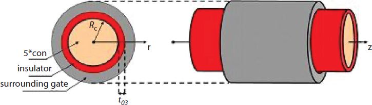
Figure 5.11 Gate-all-around nanowire-MOSFET.
A GAA nanowire-MOSFET is a semiconductor device in which the gate electrodes surround the device conducting channel in all directions [77, 78]. As a result, we have improved gate controllability over the device’s channel. The GAA semiconductor device’s channel form might be triangular, rectangular, square, or polygonal. The conducting channels of this nanowire-MOSFET can be n-channel nanowire MOSFET or p-channel nanowire-MOSFET. Various MOSFET device structures have been designed, which include silicon-on-insulator MOSFET, symmetric and asymmetric double-gate MOSFET, tri-gate MOSFET and Fin-FET. Among these, GAA device structures have demonstrated the advantage of strong gate control over channel [67, 79, 80]. It has the best electrical and conductivity qualities. In practice, “nanowires” are built on a planar substrate made of semi-conductor materials such as silicon or germanium or compound materials [81–83].
The GAA nanowire-MOSFET structured devices are constructed in two configurations, namely Lateral nanowire-MOSFET (LFET) and Vertical nanowire-MOSFET (VFET). Kim et al. [84] designed LFET and VFET using 3D technology TCAD tools and the parasitic components corresponding to these MOSFETs are calculated by varying the diameter of the nano-wire. Their overall parasitic resistance is categorized into contact-resistance, extension-resistance, sheet-resistance, and spreading-resistance, and over-all parasitic capacitance is categorized into outer fringing-capacitance, overlap-capacitance, extension-capacitance, and inner fringing-capacitance [84]. The variation of these parasites with respect to variation of the diameter of the nanowire is depicted in Figures 5.12 and 5.13. The parasitic resistance in nanowire-MOSFET increases with the decrement of the diameter of the nanowire because of increment in extension-resistance, whereas the parasitic capacitance in nanowire-MOSFET decreases with the decrement of the diameter of the nanowire [84]. When the parasites of VFET and LFET are compared, LFET has more parasitic resistance and VFET has more parasitic capacitance, which can be observed from Figures 5.14 and 5.15. The parasitic resistance difference between VFET and LFET is small, but the parasitic capacitance difference is higher, resulting in VFET having a longer delay than LFET [84].

Figure 5.12 Parasitic resistance of lateral nanowire-MOSFET and vertical nanowire-MOSFET.

Figure 5.13 Parasitic capacitance of lateral nanowire-MOSFET and vertical nanowire-MOSFET.
Chenyun et al. [85] studied the performance of LFET and VFET at technology node of 5nm utilizing an ARM core CPU. The various device configurations such as nanowires, stacking of nanowires and different numbers of fins are investigated to find tradeoffs between area, frequency, energy and leakage by using multi-threshold optimization. The stress in the channel that may be induced in LFETs results in a higher ON-state current; the results show that GAA LFET core has higher maximum frequency than its VFET equivalent [85]. The LFET GAA cores are hence advantageous for rapid timing targets [85]. When compared to LFET GAA cores with 2-stack/2-fin at the same leakage-current, the three nanowires VFET GAA cores offer a 20% energy saving and 7% area reduction for slow timing targets [85].
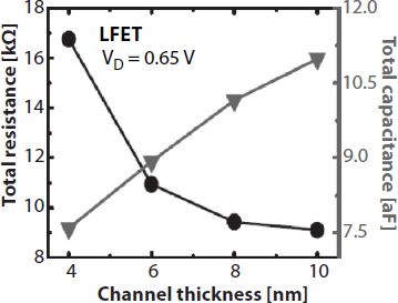
Figure 5.14 Resistance and capacitance of lateral nanowire-MOSFET during ON-state.
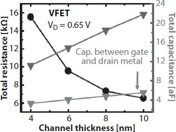
Figure 5.15 Resistance and capacitance of vertical nanowire-MOSFET during ON-state.
The nanowire MOSFET extension length tuning is presented by Kaushal et al. [86] as shown in Figure 5.16. The sub-14nm nanowire-MOSFET with tuning of extension length significantly reduces the power dissipation with a small active area; using of this in the 6-T nanowire SRAM cell improves the SRAM cell read stability. The device design parameters such as the diameter of the nanowire, the device extension length, source-drain dop-ing and channel doping are utilized to improve the stability of the SRAM cells. The impact of these design parameters on ON-state and OFF-state current for various extension lengths are studied [86] and depicted in Figures 5.17, 5.18 and 5.19. It is observed that the extension length tuning technique exhibits ~60% and 15% savings in static power consumption and active area [86], respectively, in comparison with a conventional nanowire-stack tuning technique. Furthermore, the hold and read noise margins are improved by 8% and 6% with the proposed technique, respectively.
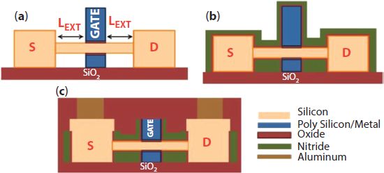
Figure 5.16 (a) silicon nanowire-MOSFET with extension, (b) silicon nanowire-MOSFET with extension and spacer, (c) silicon nanowire-MOSFET with extension, spacer and raised source-drain.
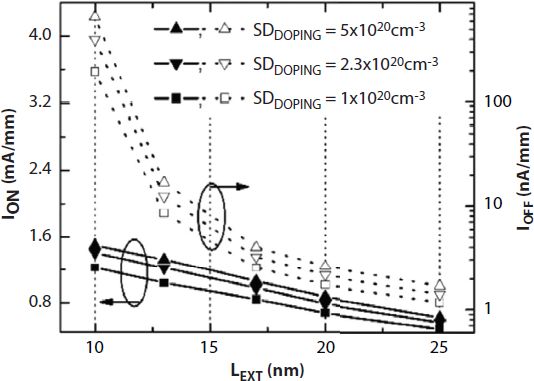
Figure 5.17 Source-drain doping concentration impact on ON-state current and OFF-state current.
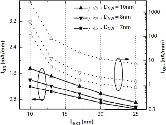
Figure 5.18 Diameter of the nanowire impact on ON-state current and OFF-state current.

Figure 5.19 Channel doping concentration impact on ON-state current and OFF-state current.
The vertical nanowire-MOSFET with channel engineering is reported by Chen et al. [87] to achieve multi-threshold voltage. The usage of asym-metrical source halo doping or asymmetrical drain halo doping results in this multi-threshold voltage. The 3D and 2D cross-sectional view of asymmetrical source halo VFET is illustrated in Figure 5.20. By keeping the appropriate halo doping concentration, we can achieve at least three different threshold voltages and it also leads to controlling of leakage currents which can be observed from Figures 5.21 and 5.22. The results show that halo configuration close to source side exhibits larger threshold voltage tuning range and better SCE controlling [87]. Moreover, adjustment of halo doping concentration along with nanowire diameter can be a better choice for proper adjustment of threshold voltage for 7nm technology node [87].

Figure 5.20 (a) 3-dimensional and (b) 2-dimensional view of source-halo vertical nanowire-MOSFET.

Figure 5.21 Impact of halo doping concentation on threshold voltage.
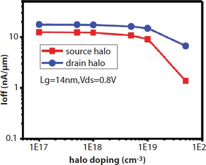
Figure 5.22 Impact of halo doping concentation on OFF-state current.
Further, Chen et al. [88] proposed asymmetric doping profile nanowire-MOSFET for enhancement of ON-state current. This VFET device utilizes extension region and spacer material with asymmetric doping profile as illustrated in Figure 5.23. The performance of this is analyzed for various spacer materials, spacer lengths as well as different doping profiles. As compared to lightly doped Source-drain and heavily doped Source-drain, Asymmetric-Graded-Lightly-Doped-Drain (AGLDD) exhibits higher ON-state current without affecting leakage as shown in Figures 5.24 and 5.25 [88]. Moreover, higher ON-state current and SCE immunity can be accomplished while parasitic capacitance can be kept within acceptable limits by using high-k spacer material and optimal drain spacer width [88]. This approach can be used to design low-power vertical channel nanowire FETs.
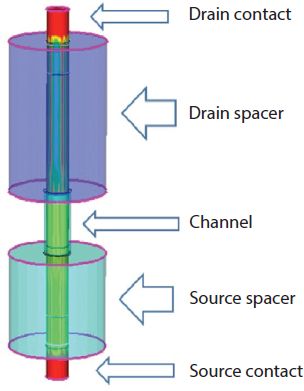
Figure 5.23 3-dimensional asymmetrical structure of vertical nanowire MOSFET.

Figure 5.24 Impact of three varieties of doping profiles on ON-state current for various diameters of the nanowire.
In addition, Goel et al. [89] proposed a Dual-Metal nanowire MOSFET (DM-NWFET) as shown in Figure 5.26. Two different work functions, i.e., a lower work function metal gate on the drain side and a higher work function metal gate on the source side is used in DM-NWFET. Dual metal was built using Molybdenum (Mo) as the gate material and its work function can be altered by manipulating the doping implant in Molybdenum [89].GIDL is a leakage condition caused by minority carriers tunneling into the drain region. The applying of two different work functions causes deviation in the electric potential along the channel leading to the change in the electric field over the channel. The field aberration causes bending between the drain and gate regions, resulting in a release of minority carriers in the OFF-state as the GIDL current. Keeping the lower work function to the Gate2 in DM-NWFET decreases the velocity of electron and leads to reduction in tunneling of minority carriers during OFF-state. It therefore results in reduction of gate leakage [89–91].

Figure 5.25 Impact of three varieties of doping profiles on OFF-state current for various diameters of the nanowire.

Figure 5.26 2-dimensional cross-sectional view dual metal nanowire-MOSFET.
5.7 Conclusion
In this review paper, we have observed the innovations in the structure of MOSFET as the device is scaled down to the sub-5nm node. Initially, as the MOSFET scaling reached to sub-100 nm regime, the channel in MOSFET is behaving like a short-channel which led to SCEs resulting in higher leakage current. It is overcome by an increase in the channel doping or usage of high-k oxides or usage of metal gate in conventional MOSFET. As the device is further scaled and reached to sub-45nm node, the severity in SCE is controlled by either single-gate thin-body SOI-MOSFET or doublegate thin-body SOI-MOSFET. At 22nm technology node, a new structure Fin-FET is proposed to overcome the limitations of SOI-MOSFETs, such as floating body, kink effect. The Fin-FET devices are constructed using multi-gate structures, i.e., double-gate, tri-gate, pi-gate, omega-gate and GAA, and the controllability on the channel is increased as we moved from double-gate to GAA. Furthermore, the GAA nanowire-MOSFETs are proposed due to their better electrical characteristics than Fin-FETs in the sub-10nm regime. The performance of conventional nanowire-MOSFETs is further improved by adding spacer material, extension layers, halo-doping and dual-metal. The nanowire-MOSFET exhibits lower leakage, higher drive current, near-ideal subthreshold swing and lower DIBL at sub-5nm regime as compared to other MOSFET structures.
References
- 1. Saha, S. K. (2015). Compact models for integrated circuit design: conventional transistors and beyond. Taylor & Francis.
- 2. Saha, S. K. (2018). Transitioning semiconductor companies enabling smart environments and integrated ecosystems. Open Journal of Business and Management, 6(2), 428-437.
- 3. Vermesan, O., Friess, P., Guillemin, P., Sundmaeker, H., Eisenhauer, M., Moessner, K., ... & Cousin, P. (2013). Internet of things strategic research and innovation agenda. In Internet of things: converging technologies for smart environments and integrated ecosystems, 7-152.
- 4. Saha, S. K. (2015). Emerging business trends in the microelectronics industry. Open Journal of Business and Management, 4(1), 105-113.
- 5. Shockley, W. (1998). Semiconductor Amplifier Patent. Proceedings of the IEEE, 86(1), 34-36.
- 6. Brattain, W. H., & Gibney, R. B. (1950). U.S. Patent No. 2,524,034. Washington, DC: U.S. Patent and Trademark Office.
- 7. Kilby, J. S. (2007). Miniaturized electronic circuits [US Patent no. 3,138, 743]. IEEE Solid-State Circuits Society Newsletter, 12(2), 44-54.
- 8. Kilby, J. S. (1976). Invention of the integrated circuit. IEEE Transactions on Electron Devices, 23(7), 648-654.
- 9. Kahng, D. (1960). Silicon-silicon dioxide field induced surface devices. In the Solid State Device Research Conf., Pittsburgh, PA. June 1960.
- 10. Dawon, K. (1963). U.S. Patent No. 3,102,230. Washington, DC: U.S. Patent and Trademark Office.
- 11. Wanlass, F. M. (1967). U.S. Patent No. 3,356,858. Washington, DC: U.S. Patent and Trademark Office.
- 12. Moore, G. E. (1965). Cramming more components onto integrated circuits.
- 13. Dennard, R. H., Gaensslen, F. H., Yu, H. N., Rideout, V. L., Bassous, E., & LeBlanc, A. R. (1974). Design of ion-implanted MOSFET’s with very small physical dimensions. IEEE Journal of solid-state circuits, 9(5), 256-268.
- 14. Roy, K., Mukhopadhyay, S., & Mahmoodi-Meimand, H. (2003). Leakage current mechanisms and leakage reduction techniques in deep-submicrometer CMOS circuits. Proceedings of the IEEE, 91(2), 305-327.
- 15. Wong, H. S. (2002). Beyond the conventional transistor. IBM Journal of Research and Development, 46(2.3), 133-168.
- 16. Critchlow, D. L. (1999). MOSFET scaling-the driver of VLSI technology. Proceedings of the IEEE, 87(4), 659-667.
- 17. Kuhn, K. J. (2012). Considerations for ultimate CMOS scaling. IEEE transactions on Electron Devices, 59(7), 1813-1828.
- 18. Arora, N. D. (2012). MOSFET models for VLSI circuit simulation: theory and practice. Springer Science & Business Media.
- 19. Chauhan, Y. S., Lu, D., Venugopalan, S., Khandelwal, S., Duarte, J. P., Paydavosi, N., ... & Hu, C. (2015). FinFET modeling for IC simulation and design: using the BSIM-CMG standard. Academic Press.
- 20. Bertrand, G., Deleonibus, S., Previtali, B., Guegan, G., Jehl, X., Sanquer, M., & Balestra, F. (2004). Towards the limits of conventional MOSFETs: case of sub 30 nm NMOS devices. Solid-State Electronics, 48(4), 505-509.
- 21. Saha, S. (1998). Effects of inversion layer quantization on channel profile engineering for nMOSFETs with 0.1 μm channel lengths. Solid-State Electronics, 42(11), 1985-1991.
- 22. Saha, S. K. (2001). U.S. Patent No. 6,323,520. Washington, DC: U.S. Patent and Trademark Office.
- 23. Saha, S. K. (1999, September). Drain profile engineering for MOSFET devices with channel lengths below 100 nm. In Microelectronic Device Technology III (Vol. 3881, pp. 195-204). SPIE.
- 24. Saha, S. K. (2002). U.S. Patent No. 6,344,405. Washington, DC: U.S. Patent and Trademark Office.
- 25. Saha, S. (2001). Scaling considerations for high performance 25 nm metal– oxide–semiconductor field effect transistors. Journal of Vacuum Science & Technology B: Microelectronics and Nanometer Structures Processing, Measurement, and Phenomena, 19(6), 2240-2246.
- 26. Saha, S. (2001). Design considerations for 25 nm MOSFET devices. Solid-State Electronics, 45(10), 1851-1857.
- 27. Radosavljevic, M., Chu-Kung, B., Corcoran, S., Dewey, G., Hudait, M. K., Fastenau, J. M., ... & Chau, R. (2009, December). Advanced high-K gate dielectric for high-performance short-channel In 0.7 Ga 0.3 As quantum well field effect transistors on silicon substrate for low power logic applications. In 2009 IEEE International Electron Devices Meeting (IEDM) (pp. 1-4). IEEE.
- 28. Caymax, M., Eneman, G., Bellenger, F., Merckling, C., Delabie, A., Wang, G.,... & Heyns, M. (2009, December). Germanium for advanced CMOS anno 2009: A SWOT analysis. In 2009 IEEE International Electron Devices Meeting (IEDM) (pp. 1-4). IEEE.
- 29. Schwierz, F. (2010). Graphene transistors. Nature Nanotechnology, 5(7), 487-496.
- 30 Radisavljevic, B., Radenovic, A., Brivio, J., Giacometti, V., & Kis, A. (2011). Single-layer MoS2 transistors. Nature Nanotechnology, 6(3), 147-150.
- 31. Jeon, K., Loh, W. Y., Patel, P., Kang, C. Y., Oh, J., Bowonder, A., ... & Hu, C. (2010, June). Si tunnel transistors with a novel silicided source and 46mV/ dec swing. In 2010 Symposium on VLSI Technology (pp. 121-122). IEEE.
- 32. Islam Khan, A., Bhowmik, D., Yu, P., Joo Kim, S., Pan, X., Ramesh, R., & Salahuddin, S. (2011). Experimental evidence of ferroelectric negative capacitance in nanoscale heterostructures. Applied Physics Letters, 99(11), 113501.
- 33. Radosavljevic, M., Dewey, G., Basu, D., Boardman, J., Chu-Kung, B., Fastenau, J. M., ... & Chau, R. (2011, December). Electrostatics improvement in 3-D tri-gate over ultra-thin body planar InGaAs quantum well field effect transistors with high-K gate dielectric and scaled gate-to-drain/gate-to-source separation. In 2011 International Electron Devices Meeting (pp. 33-1). IEEE.
- 34. Tomioka, K., Yoshimura, M., & Fukui, T. (2012, June). Steep-slope tunnel field-effect transistors using III–V nanowire/Si heterojunction. In 2012 symposium on VLSI technology (VLSIT) (pp. 47-48). IEEE.
- 35. Fujita, K., Torii, Y., Hori, M., Oh, J., Shifren, L., Ranade, P., ... & Ema, T. (2011, December). Advanced channel engineering achieving aggressive reduction of V T variation for ultra-low-power applications. In 2011 International Electron Devices Meeting (pp. 32-3). IEEE.
- 36. Saha, S. (2016). U.S. Patent No. 9,299,702. Washington, DC: U.S. Patent and Trademark Office.
- 37. Saha, S. K. (2017). U.S. Patent No. 9,768,074. Washington, DC: U.S. Patent and Trademark Office.
- 38. Bohr, M. T., Chau, R. S., Ghani, T., & Mistry, K. (2007). The high-k solution. IEEE spectrum, 44(10), 29-35.
- 39. Subramanian, V., Kedzierski, J., Lindert, N., Tam, H., Su, Y., McHale, J., ... & Hu, C. (1999, June). A bulk-Si-compatible ultrathin-body SOI technology for sub-100 nm MOSFETs. In 1999 57th Annual Device Research Conference Digest (Cat. No. 99TH8393) (pp. 28-29). IEEE.
- 40. Balestra, F. (2013, June). Challenges and limits for very low energy computation. In 2012 IEEE 11th International Conference on Solid-State and Integrated Circuit Technology (pp. 1-4). IEEE.
- 41. Cristoloveanu, S., & Balestra, F. (2009). Introduction to SOI technology and transistors. In Physics and operation of Silicon devices and Integrated circuits.
- 42. Choi, Y. K., Asano, K., Lindert, N., Subramanian, V., King, T. J., Bokor, J., & Hu, C. (1999, December). Ultra-thin body SOI MOSFET for deep-sub-tenth micron era. In International Electron Devices Meeting 1999. Technical Digest (Cat. No. 99CH36318) (pp. 919-921). IEEE.
- 43. Liu, Q., Yagishita, A., Loubet, N., Khakifirooz, A., Kulkarni, P., Yamamoto, T., ... & Sampson, R. (2010, June). Ultra-thin-body and BOX (UTBB) fully depleted (FD) device integration for 22nm node and beyond. In 2010 Symposium on VLSI Technology (pp. 61-62). IEEE.
- 44. Yoo, D. W., & Joshi, Y. K. (2004). Energy efficient thermal management of electronic components using solid-liquid phase change materials. IEEE Transactions on Device and Materials Reliability, 4(4), 641-649.
- 45. Suzuki, E., Ishii, K., Kanemaru, S., Maeda, T., & Tsutsumi, T. Member IEEE, T. Sekigawa, K. Nagai, and H. Hiroshima 2000. IEEE Trans. Electron Devices, 47, 354.
- 46. Liu, Q., Vinet, M., Gimbert, J., Loubet, N., Wacquez, R., Grenouillet, L., ... & Sampson, R. (2013, December). High performance UTBB FDSOI devices featuring 20nm gate length for 14nm node and beyond. In 2013 IEEE International Electron Devices Meeting (pp. 9-2). IEEE.
- 47. Barral, V., Poiroux, T., Andrieu, F., Buj-Dufournet, C., Faynot, O., Ernst, T., ... & Deleonibus, S. (2007, December). Strained FDSOI CMOS technology scalability down to 2.5 nm film thickness and 18nm gate length with a TiN/ HfO 2 gate stack. In 2007 IEEE International Electron Devices Meeting (pp. 61-64). IEEE.
- 48. Cheng, K., Khakifirooz, A., Kulkarni, P., Kanakasabapathy, S., Schmitz, S., Reznicek, A., ... & O’Neill, J. (2009, June). Fully depleted extremely thin SOI technology fabricated by a novel integration scheme featuring implant-free, zero-silicon-loss, and faceted raised source/drain. In 2009 Symposium on VLSI Technology (pp. 212-213). IEEE.
- 49. Faynot, O., Andrieu, F., Weber, O., Fenouillet-Béranger, C., Perreau, P., Mazurier, J., ... & Deleonibus, S. (2010, December). Planar Fully depleted SOI technology: A Powerful architecture for the 20nm node and beyond. In 2010 International Electron Devices Meeting (pp. 3-2). IEEE.
- 50. Wong, H. S., Frank, D. J., & Solomon, P. M. (1998, December). Device design considerations for double-gate, ground-plane, and single-gated ultra-thin SOI MOSFET’s at the 25 nm channel length generation. In International Electron Devices Meeting 1998. Technical Digest (Cat. No. 98CH36217) (pp. 407-410). IEEE.
- 51. Suzuki, K., Tanaka, T., Tosaka, Y., Horie, H., & Arimoto, Y. (1993). Scaling theory for double-gate SOI MOSFET’s. IEEE Transactions on Electron Devices, 40(12), 2326-2329.
- 52. Auth, C., Allen, C., Blattner, A., Bergstrom, D., Brazier, M., Bost, M., ... & Mistry, K. (2012, June). A 22nm high performance and low-power CMOS technology featuring fully-depleted tri-gate transistors, self-aligned contacts and high density MIM capacitors. In 2012 symposium on VLSI technology (VLSIT) (pp. 131-132). IEEE.
- 53. Merritt, R. (2012). TSMC taps ARM’s V8 on road to 16-nm FinFET. EE Times..
- 54. Hisamoto, D., Lee, W. C., Kedzierski, J., Takeuchi, H., Asano, K., Kuo, C., ... & Hu, C. (2000). FinFET-a self-aligned double-gate MOSFET scalable to 20 nm. IEEE Transactions on Electron Devices, 47(12), 2320-2325.
- 55. Natarajan, S., Agostinelli, M., Akbar, S., Bost, M., Bowonder, A., Chikarmane, V., ... & Zhang, K. (2014, December). A 14nm logic technology featuring 2 nd-generation finfet, air-gapped interconnects, self-aligned double patterning and a 0.0588 µm 2 sram cell size. In 2014 IEEE International Electron Devices Meeting (pp. 3-7). IEEE.
- 56. James, D. (2012, September). Intel Ivy Bridge unveiled—The first commercial tri-gate, high-k, metal-gate CPU. In Proceedings of the IEEE 2012 Custom Integrated Circuits Conference (pp. 1-4). IEEE..
- 57. Kedzierski, J., Ieong, M., Nowak, E., Kanarsky, T. S., Zhang, Y., Roy, R., ... & Wong, H. S. (2003). Extension and source/drain design for high-performance FinFET devices. IEEE Transactions on Electron Devices, 50(4), 952-958.
- 58. Razavieh, A., Zeitzoff, P., & Nowak, E. J. (2019). Challenges and limitations of CMOS scaling for FinFET and beyond architectures. IEEE Transactions on Nanotechnology, 18, 999-1004.
- 59. Zheng, P., Connelly, D., Ding, F., & Liu, T. J. K. (2015). FinFET evolution toward stacked-nanowire FET for CMOS technology scaling. IEEE Transactions on Electron Devices, 62(12), 3945-3950.
- 60. Iwai, H., Natori, K., Kakushima, K., Ahmet, P., Oshiyama, A., Shiraishi, K., ... & Ohmori, K. (2010, September). Si nanowire device and its modeling. In 2010 International Conference on Simulation of Semiconductor Processes and Devices (pp. 63-66). IEEE.
- 61. Ziegler, A., & Luisier, M. (2018). Complex Band Structure Effects in k.p-Based Quantum Transport Simulations of p-Type Silicon Nanowire Transistors. IEEE Transactions on Electron Devices, 65(4), 1298-1302.
- 62. Colinge, J. P., Lee, C. W., Afzalian, A., Akhavan, N. D., Yan, R., Ferain, I., ... & Murphy, R. (2010). Nanowire transistors without junctions. Nature Nanotechnology, 5(3), 225-229.
- 63. Bangsaruntip, S., Cohen, G. M., Majumdar, A., & Sleight, J. W. (2010). Universality of short-channel effects in undoped-body silicon nanowire MOSFETs. IEEE Electron Device Letters, 31(9), 903-905.
- 64. Takato, H., Sunouchi, K., Okabe, N., Nitayama, A., Hieda, K., Horiguchi, F., & Masuoka, F. (1991). Impact of surrounding gate transistor (SGT) for ultra-high-density LSI’s. IEEE Transactions on Electron Devices, 38(3), 573-578.
- 65. Nitayama, A., Takato, H., Okabe, N., Sunouchi, K., Hieda, K., Horiguchi, F., & Masuoka, F. (1991). Multi-pillar surrounding gate transistor (M-SGT) for compact and high-speed circuits. IEEE Transactions on Electron Devices, 38(3), 579-583.
- 66. Watanabe, S., Tsuchida, K., Takashima, D., Oowaki, Y., Nitayama, A., Hieda, K., ... & Hara, H. (1995). A novel circuit technology with surrounding gate transistors (SGT’s) for ultra high density DRAM’s. IEEE Journal of Solid-State Circuits, 30(9), 960-971.
- 67. Colinge, J. P. (2004). Multiple-gate soi mosfets. Solid-state Electronics, 48(6), 897-905.
- 68. Yan, R. H., Ourmazd, A., & Lee, K. F. (1992). Scaling the Si MOSFET: From bulk to SOI to bulk. IEEE Transactions on Electron Devices, 39(7), 1704-1710.
- 69. Yakimets, D., Eneman, G., Schuddinck, P., Bao, T. H., Bardon, M. G., Raghavan, P., ... & De Meyer, K. (2015). Vertical GAAFETs for the ultimate CMOS scaling. IEEE Transactions on Electron Devices, 62(5), 1433-1439.
- 70. Yang, F. L., Lee, D. H., Chen, H. Y., Chang, C. Y., Liu, S. D., Huang, C. C., ...& Hu, C. (2004, June). 5nm-gate nanowire FinFET. In Digest of Technical Papers. 2004 Symposium on VLSI Technology, 2004. (pp. 196-197). IEEE.
- 71. Singh, N., Lim, F. Y., Fang, W. W., Rustagi, S. C., Bera, L. K., Agarwal, A., ... & Kwong, D. L. (2006, December). Ultra-narrow silicon nanowire gate-all-around CMOS devices: Impact of diameter, channel-orientation and low temperature on device performance. In 2006 International Electron Devices Meeting (pp. 1-4). IEEE.
- 72. Suk, S. D., Lee, S. Y., Kim, S. M., Yoon, E. J., Kim, M. S., Li, M., ... & Ryu, B. I. (2005, December). High performance 5nm radius Twin Silicon Nanowire MOSFET (TSNWFET): fabrication on bulk si wafer, characteristics, and reliability. In IEEE International Electron Devices Meeting, 2005. IEDM Technical Digest. (pp. 717-720). IEEE.
- 73. Yeo, K. H., Suk, S. D., Li, M., Yeoh, Y. Y., Cho, K. H., Hong, K. H., ... & Ryu, B. I. (2006, December). Gate-all-around (GAA) twin silicon nanowire MOSFET (TSNWFET) with 15 nm length gate and 4 nm radius nanowires. In 2006 International Electron Devices Meeting (pp. 1-4). IEEE.
- 74. Singh, N., Lim, F. Y., Fang, W. W., Rustagi, S. C., Bera, L. K., Agarwal, A., ... & Kwong, D. L. (2006, December). Ultra-narrow silicon nanowire gate-all-around CMOS devices: Impact of diameter, channel-orientation and low temperature on device performance. In 2006 International Electron Devices Meeting (pp. 1-4). IEEE.
- 75. Jiang, Y., Liow, T. Y., Singh, N., Tan, L. H., Lo, G. Q., Chan, D. S. H., & Kwong, D. L. (2008, June). Performance breakthrough in 8 nm gate length gate-all-around nanowire transistors using metallic nanowire contacts. In 2008 Symposium on VLSI Technology (pp. 34-35). IEEE.
- 76. Tian, Y., Huang, R., Wang, Y., Zhuge, J., Wang, R., Liu, J., ... & Wang, Y. (2007, December). New self-aligned silicon nanowire transistors on bulk substrate fabricated by epi-free compatible CMOS technology: Process integration, experimental characterization of carrier transport and low frequency noise. In 2007 IEEE International Electron Devices Meeting (pp. 895-898). IEEE.
- 77. Ishikawa, F., & Buyanova, I. (Eds.). (2017). Novel compound semiconductor nanowires: materials, devices, and applications. CRC Press.
- 78. Park, J. T., & Colinge, J. P. (2002). Multiple-gate SOI MOSFETs: device design guidelines. IEEE Transactions on Electron Devices, 49(12), 2222-2229.
- 79. Sun, X., Moroz, V., Damrongplasit, N., Shin, C., & Liu, T. J. K. (2011). Variation study of the planar ground-plane bulk MOSFET, SOI FinFET, and trigate bulk MOSFET designs. IEEE Transactions on Electron Devices, 58(10), 3294-3299.
- 80. Li, C., Zhuang, Y., & Han, R. (2011). Cylindrical surrounding-gate MOSFETs with electrically induced source/drain extension. Microelectronics Journal, 42(2), 341-346.
- 81. Lieber, C. M. (2011). Semiconductor nanowires: A platform for nanoscience and nanotechnology. MRS Bulletin, 36(12), 1052-1063.
- 82. Jena, B., Dash, S., & Mishra, G. P. (2016). Electrostatic performance improvement of dual material cylindrical gate MOSFET using work-function modulation technique. Superlattices and Microstructures, 97, 212-220.
- 83. Ramkrishna, B. S., Jena, B., Dash, S., & Mishra, G. P. (2017). Investigation of electrostatic performance for a conical surrounding gate MOSFET with linearly modulated work-function. Superlattices and Microstructures, 101, 152-159.
- 84. Kim, M., Ko, H., Kang, M., & Shin, H. (2017, June). Comparison of parasitic components between LFET and VFET using 3D TCAD. In 2017 Silicon Nanoelectronics Workshop (SNW) (pp. 91-92). IEEE..
- 85. Pan, C., Raghavan, P., Yakimets, D., Debacker, P., Catthoor, F., Collaert, N., ... & Naeemi, A. (2015). Technology/system codesign and benchmarking for lateral and vertical GAA nanowire FETs at 5-nm technology node. IEEE Transactions on Electron Devices, 62(10), 3125-3132.
- 86. Kaushal, G., Jeong, H., Maheshwaram, S., Manhas, S. K., Dasgupta, S., & Jung, S. O. (2015). Low power SRAM design for 14 nm GAA Si-nanowire technology. Microelectronics Journal, 46(12), 1239-1247.
- 87. Chen, G., Li, M., Fan, J., Yang, Y., Zhang, H., & Huang, R. (2016, May). Multi-V T design of vertical channel nanowire FET for sub-10nm technology node. In 2016 IEEE International Nanoelectronics Conference (INEC) (pp. 1-2). IEEE.
- 88. Chen, G., Li, M., Zhang, J., Yang, Y., & Huang, R. (2016, October). Source/ drain architecture design of vertical channel nanowire FET for sub-10nm node. In 2016 13th IEEE International Conference on Solid-State and Integrated Circuit Technology (ICSICT) (pp. 1008-1010). IEEE.
- 89. Goel, A., Rewari, S., Verma, S., & Gupta, R. S. (2019). Temperature-dependent gate-induced drain leakages assessment of dual-metal nanowire field-effect transistor—analytical model. IEEE Transactions on Electron Devices, 66(5), 2437-2445.
- 90. Mendiratta, N., Tripathi, S.L. & Chander, S. Analytical Model of Dopingless Asymmetrical Junctionless Double Gate MOSFET. Silicon (2022). https://doi.org/10.1007/s12633-022-01819-z.
- 91. Verma, S., Tripathi, S.L. Impact & Analysis of Inverted-T shaped Fin on the Performance parameters of 14-nm heterojunction FinFET. Silicon (2022). https://doi.org/10.1007/s12633-022-01708-5.
Note
- * Corresponding author: [email protected]