
3
Machine Learning–Based VLSI Test and Verification
Jyoti Kandpal*
Dept. of Electronics and Communication Engineering, National Institute of Technology Arunachal Pradesh, Pradesh, India
Abstract
To test Integrated Chips, test pattern generation and fault simulation are vital. Testing verifies a circuit’s accuracy regarding gates and connections between them. The fundamental purpose of testing is to model the circuit’s various activities. Several Electronic Design Automation tools for fault identification and test pattern development are available to simulate circuits for structural testing. This chapter gives a brief idea of machine learning techniques: defect identification and test pattern generation at various abstraction levels.
Keywords: VLSI testing, Electronic Design Automation (EDA), machine learning
3.1 Introduction
With the emergence of complementary metal-oxide-semiconductor (CMOS) technology, a new circuit design paradigm with low power consumption emerged. CMOS design techniques are frequently used for digital circuits with particularly large-scale integration (VLSI). Today’s IC chips have billions of transistors on a single die. In addition to design, testing for manufacturing flaws is an essential component in the production cycle of digital IC chips since it affects dependability, cost, and delivery time. Effective testing is also essential to determine the chip’s yield and information on process variations. Various areas of fault modelling, detection, diagnosis, fault simulation, built-in self-test, and design-for-testability (DFT) have been extensively researched over the last three decades, resulting in fast test generation and fault-diagnostic algorithms testable designs. Several industrial tools for testing have been developed over the years. However, with the increasing sophistication of IC chips, the obstacles in testing, especially in diagnosis, have grown [1].
VLSI testing is an integral part of any design because it allows you to determine if there are any defects in the circuit. The accuracy of the circuit can be established through testing. Verification is another approach to testing a circuit’s behavior. The significant distinction between testing and verification is that testing considers a circuit, whilst verification considers the design. The distinction between testing and verification is seen in Table 3.1.
The verification process is divided into two parts:
- Simulation-based verification
- Formal approaches
VLSI testing covers the full range of testing methods and structures integrated into a system-on-chip (SOC) to ensure manufactured devices’ quality during manufacturing tests. Test methods often comprise malfunction simulation and test generation to provide quality test patterns to each device. In addition, the test structures frequently use particular design for testability (DFT) techniques to test the digital logic sections of the device, such as scan design and built-in self-test (BIST). As the issue gets identified, the company’s testing costs for the final product will be reduced. The “Rule of Ten” is commonly used in the VLSI testing sector. It claims that as the testing phase progresses from one step to the next (Chip level > Board level > System-level > System-level at the field), the expense of identifying a flaw increases by a factor of ten. VLSI testing at various abstraction levels is depicted in Figure 3.1.
Table 3.1 Difference between testing and verification.
| Testing | Verification |
|---|---|
| Verifies the correctness of a manufactured hardware. | In this process verifies the correctness of a circuit. |
Testing is a two-step process:
| They were performed by simulation or hardware emulation or formal methods. |
| Test application performed on every manufactured device. | They executed one prior manufacturing. |
| Responsible for the quality of the device. | Responsible for quality of design. |

Figure 3.1 Stages of VLSI testing [1].
3.2 The VLSI Testing Process
There are two methods of the testing process.
3.2.1 Off-Chip Testing
The chip test equipment provides an external toolkit for this type of testing. Automated Test Equipment (ATE) is an example of Off-chip testing.
3.2.2 On-Chip Testing
In this method, test equipment is added on-chip and embedded resources to detect any flaw or defect in the circuit.
Equation 3.1 represents the testing formula that is followed in the industry [2]
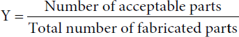
Y is the yield or the ratio of acceptance of the parts. In the initial phase, when the technology is new, the output is as low as 10%, but when the technology attains a certain level of maturity, it grows to a staggering 95%. Figure 3.2 represents VLSI testability and reliability.
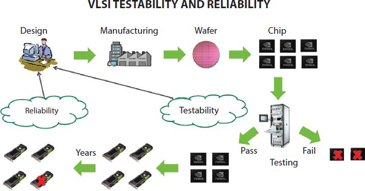
Figure 3.2 Example of VLSI testability and reliability [3].
In circuit-level testing is divided into two categories furthermore:
3.2.3 Combinational Circuit Testing
3.2.3.1 Fault Model
Fault Model (Stuck at model):
- This method assumes selected wires (gate input or output) is stuck at logic 0 or 1.
- It is a simplistic model and requires 2 n test input for n input circuit but for practical purposes in real life; it requires many test inputs.
3.2.3.2 Path Sensitizing
In this method, multi-wire testing is used in a circuit at the same time.
3.2.4 Sequential Circuit Testing
3.2.4.1 Scan Path Test
In this method, multiplexers are used to pass the FF inputs.
3.2.4.2 Built-In-Self Test (BIST)
In this method, a pseudorandom test vector is used in the feedback shift register.
3.2.4.3 Boundary Scan Test (BST)
In this tests interconnect (wire lines) on printed circuit boards or sub-blocks inside an integrated circuit. Boundary scan is also widely used as a debugging method to watch integrated circuit pin states, measure voltage, or analyze sub-blocks inside an integrated circuit.
3.2.5 The Advantages of VLSI Testing
- The complex testing process can be eliminated for PCB testing to minimize human intervention.
- It eases the job of the test engineer and increases the efficiency multifold.
- Drastically reduces the time spent on complex testing.
- The coverage for all types of faults is expanded heavily.
Compared to IC design capability, integrated circuit technology is rapidly advancing. The VLSI computation process is a time-consuming and complex operation. VLSI developers must monitor and implement technology growth as it occurs daily and on a periodic basis to improve their design tools. Machine learning (ML) enters the VLSI field with improved design methodology, features, and capabilities [3].
ML has several features and methods, but it still has significant limits in solving problems. Consequently, ML opens up plenty of possibilities for collaboration in VLSI and computer-based design. Furthermore, the knowledge gathered by ML is used to design and implement computer chips. As a result, it is regarded as the first ML application. In recent years, knowledge gained from ML introduction classes has been used to handle and routinely employ computer-based design tools.
Previously, most chips were developed manually, resulting in excessively huge size and slow performance. Furthermore, verifying such hand-crafted chips is a complex and time-consuming operation. Because of these complications, an automated tool was created. Furthermore, this automation tool has been upgraded to include new functionalities.
Chip designers introduce new design methods frequently, such as memory combing, novel techniques in computing tasks, etc., which must be controlled in the design process. Many manufacturers, like Synopsys, Mentor Graphics, and Cadence, offer computer-aided design (CAD) tools that can be considered machine learning applications for chip design. AI (Artificial Intelligence) and ML revolutionize every enterprise with extremely sub-stantial inputs due to technology advancement. Machine learning has made many essential modifications in the VLSI sector.
So far, ML has assisted the VLSI sector by maximizing EDA tools, which helps reduce design time and manufacturing costs. Furthermore, machine learning in VLSI design aids EDA tools in finding an optimal solution in case of scenarios by forecasting chip flaws, which saves money during manufacturing [4].
3.3 Machine Learning’s Advantages in VLSI Design
The benefits of ML in the VLSI field are as follows below.
3.3.1 Ease in the Verification Process
Machine learning in VLSI design and verification is critical as the amount of data created by complex devices continues to grow, ensuring smooth operation without compromising performance or cost. For RTL implementation, ML assists in formulating test cases and suggests better Design flows.
3.3.2 Time-Saving
Different regression methods are used in machine learning to reduce the complexity; therefore, verification time is reduced.
3.3.3 3Ps (Power, Performance, Price)
Cadence and Synopsys are two EDA systems that continually incorporate machine learning techniques to improve design stimulation and redesign the three Ps.
Figure 3.3 presents the machine learning model in the VLSI testing field.

Figure 3.3 Machine learning model for testing [2].
3.4 Electronic Design Automation (EDA)
Electronic design automation (EDA) tools routinely are required to handle billions of entities at lower levels of abstraction. Furthermore, the number of components in a design increases with refinement and abstraction levels. Therefore, these tools need to operate on voluminous data and complex models to accomplish various tasks that can be categorized as follows.
- Estimate: Typically, we need to make estimates based on incomplete information or designer-provided hints.
- Infer dependencies: The given design data can be voluminous, and finding dependencies among various input parameters can be challenging.
- Transform: We need to refine design information based on optimality criteria and constraints. It can also involve transforming a design’s behavioural, structural, and physical views. The quality of results (QoR) in accomplishing the above tasks can often be improved by statistical data analysis, learning from examples, and encapsulating the designer’s intelligence into an EDA tool.

Figure 3.4 Applications of ML in VLSI design [1].
There have been tremendous advancements in ML tools and technology in recent times. These advancements were facilitated by novel mathematical formulations and powerful computing resources that allow massive data processing. Consequently, a plethora of freely available tools to implement ML techniques and algorithms are available to us. Therefore, ML techniques are now widely employed in VLSI design. These techniques have improved the designer’s productivity, tackled complex problems more efficiently, and provided alternative solutions. Figure 3.4 reports the ML application in the VLSI field.
VLSI design is a complex process. We decompose the design process into multiple steps, starting with system-level design and culminating in chip fabrication. We can apply ML and related techniques in design implementation, verification, testing, diagnosis, and validation stages. In this chapter, we discuss the applications of ML in the following steps:
- System-Level Design
- Logic Synthesis
- Physical Design
3.4.1 System-Level Design
There are many challenges in designing state-of-the-art systems consisting of heterogeneous components such as GPUs, CPUs, and hardware accelerators. The difficulty arises due to the following reasons.
- There is no complete implementation detail of many components at the system level. Therefore, we need to estimate the performance, power, and other attributes based on some abstract models. It is complex and error-prone.
- We need to determine near-optimal system parameters for multiple objectives and constraints. Moreover, these constraints and objectives often depend on the application and change dynamically.
- Due to an increase in the number and multitude of heterogeneous components, the design space or the solution space becomes big.
- Traditional methods such as simulations are often too slow and expensive in exploring the design space for modern heterogeneous systems.
The abovementioned challenges are tackled by ML, which is discussed in the section below. Some of these challenges can be efficiently tackled by ML, as explained in the following section.
In designing a new system, we often need to choose a particular system configuration by estimating the system performance. For example, we need to select the CPU type, memory type, CPU frequency, memory size, bus type, and motherboard for a laptop. However, to make a choice, we need to predict the actual system performance. We can evaluate the system’s performance by creating a predictive model based on neural networks and linear regression. These models can accurately determine system performance utilizing only a tiny portion of the design space and data from previously built systems.
We can also estimate heterogeneous systems’ performance and power with more detail by applying ML techniques. In particular, we can measure these attributes with many test applications running on real hardware with various configurations. Furthermore, these measurements can train an ML model to produce the expected performance and power attributes for a system design parameter. After that, we can predict them for a new application running on various system configurations. Finally, we measure these values for a single structure and feed them to the ML model. Using these inputs, ML can quickly produce the estimate for various configurations with accuracy comparable to cycle-level simulators [5].
We also need to quickly estimate performance at the component level during design space exploration. For example, implementing hybrid memory architectures in scaled heterogeneous systems has advantages. We can combine nonvolatile memories (NVM) with the traditional DRAM to improve performance. To implement the hybrid memory architecture, we need to analyze the performance of various configurations. Traditionally, architectural-level memory simulators are used in these analyses. However, this approach suffers from long simulation time and inadequate design space exploration.
A better technique is to build an ML model that predicts various figures of merit for a memory. Then, we can train the ML model by a small set of simulated memory configurations. These predictive models can quickly report latency, bandwidth, power consumption, and other attributes for a given memory configuration.
In Sen and Imam [6], neural network, SVM, random forest (RF), and gradient boosting (GB) are tried for the ML model. It is reported that the SVM and RF methods yielded better accuracies compared with other models [6].
3.4.2 Logic Synthesis and Physical Design
Logic synthesis and physical design are the main tasks in the VLSI design flow. Due to computational complexity, we divide them into multiple steps. Some key steps are multi-level logic synthesis, budgeting, technology mapping, timing optimization, chip planning, placement, clock network synthesis, and routing. Nevertheless, each of these steps is still computationally difficult. Typically, EDA tools employ several heuristics to obtain a solution. Tool options and user-specified settings guide the heuristics. The QoR (Quality of Results) strongly depends on them. These steps are sequential. Therefore, the solution produced by a step impacts all subsequent tasks. A designer often adjusts the tool settings and inputs based on experience and intuition to achieve the desired QoR [7–10].
As explained in the following paragraphs, we can reduce design effort in these tasks and improve the QoR by employing ML tools and techniques.
One of the earliest attempts to reduce design effort using ML was Learning Apprentice for VLSI design (LEAP). LEAP acquires knowledge and learns rules by observing a designer and analyzing the problem-solving steps during their activities. Subsequently, it provides advice to the designer on design refinement and optimization. A designer can accept LEAP’s advice or ignore it and manually carry out transformations. When a designer ignores the advice, LEAP considers it a training sample and updates its rule.
An ML-based tool for logic synthesis and physical design, such as a design advisor, needs to consider implementing the following tasks [11–14].
- Developing a training set consists of data points with a design problem and its corresponding solution. For example, a data point can be an initial netlist, constraints, cost function, optimization settings, and the final netlist. We need to generate these data points for training or can acquire them from designers.
- Reduced representations of the training set: The training data points typically contain many features. However, for efficient learning, we can reduce the dimensionality of the training set. For example, we can perform PCA and retain the most relevant input features.
- Learning to produce the optimum output: The training data points that we collect from the existing EDA tools are, typically, not the mathematical optimum. On the other hand, these tools give the best possible solution that could be acceptable to the designers. Therefore, training data does not represent the ground truth of the problem. Moreover, data can be sparse and biased because some specific tools generate those results. We can employ statistical models such as Bayesian neural networks (BNNs) to tackle this problem. BNNs have weights and biases specified as distributions instead of scalar values. Therefore, it can tackle disturbances due to noisy or incomplete training sets.
- Dynamic updates: We expect the ML-based design adviser to continue learning from the new design problems. We can use reinforcement learning to adjust the model dynamically.
3.4.3 Test, Diagnosis, and Validation
ML techniques also imply post-fabrication testing, diagnosis of failures, and validation of functionality. The ability of ML models to work efficiently on large data sets can be helpful in these applications [15, 16].
We can reduce the test cost by removing redundant tests. We can use ML to mine the test set and eliminate the redundant tests. We can consider a test redundant if we can predict its output using other tests that we are not removing. For example, we can use a statistical learning methodology based on decision trees to eliminate redundant tests. We should ensure maintaining product quality and limiting yield loss while removing difficulties.
We can also apply ML-based techniques to test analog/RF devices to reduce cost. However, it is challenging to maintain test errors in ML-based analog/RF device testing to an acceptable level. Therefore, we can adopt a two-tier test approach. For example, Stratigopoulos and Makris [17] developed a neural system-based framework that produces both the pass/fail labels and the confidence level in its prediction. If the confidence is low, traditional and more expensive specification testing is employed to reach a final decision. Thus, the cost advantage of ML-based analog/RF testing is leveraged. Note that the test quality is not sacrificed in the two-tier test approach [17]. We can employ a similar strategy for other verification problems where ML-induced errors are critical.
ML-based strategies are used to diagnose manufacturing defects. These methods provide alternatives to the traditional exploring of the causal relationship [18]. It can reduce the runtime complexity of the conventional diagnosis methods, especially for volume diagnosis. Wang and Wei [19] reported that defect locations are found for most defective chips even with highly compressed output responses.
Note that the scan chain patterns are insufficient to determine the failing flip-flop in a scan chain. Therefore, diagnosis methodologies need to identify defective scan cell(s) on a faulty scan chain. Unsupervised ML techniques based on the Bayes theorem are used to tolerate noises [20].
Another problem that can utilize the capabilities of ML is post-silicon validation. Before production, we carry out post-silicon validation to ensure that the silicon functions as expected under on-field operating conditions. For this purpose, we need to identify a small set of traceable signals for debugging and state restoration. Unfortunately, traditional techniques such as simulation take high runtime in identifying traceable signs. Alternatively, we can employ ML-based techniques for efficient signal selection. For example, we can train an ML with a few simulations runs. Subsequently, we can use this model to identify beneficial trace signals instead of employing time-consuming simulations [21].
3.5 Verification
We can employ techniques to improve and augment traditional verification methodologies in the following ways:
- Traditional verification often makes certain assumptions to simplify its implementation. Consequently, it can leave some verification holes, or we sacrifice the QoR of a design. ML-based verifications can consider a larger verification domain. Thus, they can fill these holes and make validation more robust.
- Traditional verification can take more runtime in finding patterns in a design. However, ML-based verification can search efficiently and produce results faster.
- Traditional verification employs some abstract models for a circuit. ML can augment such models or replace them.
In the following section, we will discuss the application of ML in the Verification of VLSI chips. In simulation-based logic verification, we can use ML to quickly fill the coverage holes or reduce the runtime. Traditionally, we apply randomly generated test stimuli and observe their response. In addition, we often incorporate coverage-directed test generation (CDG) to improve coverage within a time limit. However, it is challenging to predict the constraints that can produce test stimuli with a high range.
ML techniques can generate the bias that directs CDG towards improved coverage. ML techniques are added to the feedback loop of CDG to produce new directives or preferences for obtaining stimuli that fill coverage holes. The ML model can also learn dynamically and screen stimuli before sending them for verification. For example, ANN can extract features of stimuli and select only critical ones for validation. Thus, we can filter out many stimuli and accelerate the overall verification process.
Some verification steps, such as signal integrity (SI) checks, take significant runtime. At advanced process nodes, SI effects are critical. It changes the delay and slew of signals due to the coupling capacitance and switching activity in the neighboring wires. We can employ ML techniques to estimate the SI effects quickly [22].
First, we identify Applications of ML in VLSI Design parameters on which SI effects depend. Some of the parameters that impact SI effects are: nominal (without considering SI) delay and slew, clock period, resistance, coupling capacitance, toggle rate, the logical effort of the driver, and temporal alignment of victim and aggressor signals. We can train an ML model such as ANN or SVM to predict SI-induced changes in delay and slew. Since ML models can capture dependency in a high-dimensional space, we can utilize them for easy verification. However, we should ensure that the errors produced by ML models are tolerable for our verification purpose.
Another approach to estimating SI effects is using anomaly detection (AD) techniques. AD techniques are popularly employed to detect anomalies in financial transactions. However, we can train an ML model, such as a contractive autoencoder (CA), with the features of SI-free time-domain waveforms. Subsequently, we use the trained model to identify anomalies due to SI effects. We can use both unsupervised and semi-supervised AD techniques [23].
We can employ ML techniques to efficiently fix IR drop problems in an integrated circuit [24]. Traditionally, we carry out dynamic IR drop analysis at the end of design flows. Then, any IR drop problem is corrected by Engineering Change Order (ECO) based on the designer’s experience. Typically, we cannot identify and fix all the IR drop problems together. Consequently, we need to carry out dynamic IR drop analysis and ECO iteratively until we have corrected all the IR drop issues.
However, IR drop analysis takes significant runtime and the designer’s effort. We can reduce the iterations in IR drop signoff by employing ML to predict all the potential IR drop issues and fix them together. Firstly, by ML-based clustering techniques, we identify high IR drop regions. Subsequently, small regional ML-based models are built on local features. Using these regional models, IR drop problems are identified and fixed. After correcting all the violations, a dynamic IR drop check is finally done for signoff. If some violations still exist, we repeat the process till all the IR drop issues are corrected.
We can use ML techniques in physical verification for problems such as lithographic hotspot detection [25]. For example, we can efficiently detect lithographic hotspots by defining signatures of hotspots and a hierarchically refined detection flow consisting of ML kernels, ANN, and SVM. We can also employ a dictionary learning approach with an online learning model to extract features from the layout [26].
Another area where we can apply ML techniques is the technology library models. Technology libraries form the bedrock of digital VLSI design. Traditionally, timing and other attributes of normal cells are modelled in technology libraries as look-up tables. However, these attributes can be conveniently derived and compactly represented using ML techniques. Furthermore, the ML-models can efficiently exploit the intrinsic degrees of variation in the data.
Using ML techniques, Shashank Ram and Saurabh [27] discussed the effects of multi-input switching (MIS). Traditionally, we ignore MIS effects in timing analysis. Instead, we employ a delay model that assumes only a single input switching (SIS) for a gate during a transition. For SIS, the side inputs are held constant to non-controlling values. However, ignoring MIS effects can lead to overestimating or underestimating a gate delay. We have examined the impact of MIS on the delay of different types of gates under varying conditions. We can model the MIS-effect by deriving a corrective quantity called MIS-SIS difference (MSD). We obtain MIS delay by adding MSD to the conventional SIS delay under varying conditions.
There are several benefits of adopting ML-based techniques for modelling MIS effects. First, we can represent multi-dimensional data using a learning-based model compactly. It can capture the dependency of MIS effects on multiple input parameters and efficiently exploit them in compact representation. In contrast, traditional interpolation-based models have a large disk size and loading time, especially at advanced process nodes. Moreover, incorporating MIS effects in advanced delay models will require a drastic change in the delay calculator and is challenging. Therefore, we have modelled the MIS effect as an incremental corrective quantity over SIS delay. It fits easily with the existing design flows and delay calculators.
We have employed the ML-based MIS model to perform MIS-aware timing analysis. It involves reading MIS-aware timing libraries and reconstructing the original ANN. Since the ANNs are compact, the time consumed in the reconstruction of ANNs is insignificant. Subsequently, we compute the MSD for each relevant timing arc using the circuit conditions. Using MSD, we adjust the SIS delay and generate the MIS-annotated timing reports. It is demonstrated that ML-based MIS modelling can improve the accuracy of timing analysis. For example, for some benchmark circuits, traditional SIS-based delay differs from the corresponding SPICE-computed delay by 120%. However, the ML-based model produces delays with less than 3% errors. The runtime overhead of MIS-aware timing analysis is also negligible. Shashank Ram and Saurabh [27] can be extended to create a single composite MIS model for different process voltage temperature (PVT) conditions. In the future, we expect that we can efficiently represent other complicated circuit and transistor-level empirical models using ML models.
3.6 Challenges
In the previous sections, we discussed various applications of ML techniques in VLSI design. Nevertheless, some challenges are involved in adopting ML techniques in conventional design flows. ML techniques’ effectiveness in VLSI design depends on complex design data [33, 34]. Therefore, producing competitive results repeatedly on varying design data is challenging for many applications.
Moreover, training an ML model requires extracting voluminous data from a traditional or a detailed model. Sometimes it is challenging to generate such a training data set. Sometimes, these training data are far from the ground truth or contain many noises. Handling such a training set is challenging. ML-based design flows can disrupt the traditional design flows and be expensive to deploy.
Moreover, applying ML-based EDA tools may not produce expected results immediately. There is some non-determinism associated with ML-based applications. In the initial stages, there are not enough training data. Consequently, an ML-based EDA tool cannot guarantee accurate results. Therefore, adopting ML-based solutions in design flows is challenging for VLSI designers. Nevertheless, in the long run, ML-based techniques could deliver rich dividends.
3.7 Conclusion
ML offers efficient solutions for many VLSI design problems [28–32]. It is particularly suitable for complex problems for which we have readily available data to learn from and predict. With technological advancement, we expect that such design problems will increase. The advances in EDA tools will also help develop more efficient ML-specific hardware. The ML-specific hardware can accelerate the growth in ML technology. The advancement in ML technologies can further boost their applications in developing complex EDA tools. Thus, there is a synergic relationship between these two technologies. These technologies can benefit many other domains and applications in the long run.
References
- 1. Saini, S., Lata, K., & Sinha, G. R. (Eds.). (2021). VLSI and Hardware Implementations Using Modern Machine Learning Methods. CRC Press.
- 2. Rabaey, J. M., Chandrakasan, A. P., & Nikolic, B. (2002). Digital integrated circuits (Vol. 2). Englewood Cliffs: Prentice hall.
- 3. Ren M., & Mehta M. (2019). Using machine learning for VLSI testability and reliability. Nvidia.
- 4. Ozisikyilmaz, B., Memik, G., & Choudhary, A. (2008, June). Efficient system design space exploration using machine learning techniques. In 2008 45th ACM/IEEE Design Automation Conference (pp. 966-969). IEEE.
- 5. Greathouse, J. L., & Loh, G. H. (2018, November). Machine learning for performance and power modelling of heterogeneous systems. In 2018 IEEE/ACM International Conference on Computer-Aided Design (ICCAD) (pp. 1-6). IEEE.
- 6. Sen, S., & Imam, N. (2019, September). Machine learning based design space exploration for hybrid main-memory design. In Proceedings of the International Symposium on Memory Systems (pp. 480-489).
- 7. Zuluaga, M., Krause, A., Milder, P., & Püschel, M. (2012, June). “Smart” design space sampling to predict Pareto-optimal solutions. In Proceedings of the 13th ACM SIGPLAN/SIGBED International Conference on Languages, Compilers, Tools and Theory for Embedded Systems (pp. 119-128).
- 8. Liu, H. Y., & Carloni, L. P. (2013, May). On learning-based methods for design-space exploration with high-level synthesis. In Proceedings of the 50th Annual Design Automation Conference (pp. 1-7).
- 9. Mahapatra, A., & Schafer, B. C. (2014, May). Machine-learning based simulated annealer method for high level synthesis design space exploration. In Proceedings of the 2014 Electronic System Level Synthesis Conference (ESLsyn) (pp. 1-6). IEEE.
- 10. Kim, R. G., Doppa, J. R., & Pande, P. P. (2018, November). Machine learning for design space exploration and optimization of manycore systems. In 2018 IEEE/ACM International Conference on Computer-Aided Design (ICCAD) (pp. 1-6). IEEE.
- 11. Pagani, S., Manoj, P. S., Jantsch, A., & Henkel, J. (2018). Machine learning for power, energy, and thermal management on multicore processors: A survey. IEEE Transactions on Computer-Aided Design of Integrated Circuits and Systems, 39(1), 101-116.
- 12. Xiao, Y., Nazarian, S., & Bogdan, P. (2019). Self-optimizing and self-programming computing systems: A combined compiler, complex networks, and machine learning approach. IEEE Transactions on Very Large Scale Integration (VLSI) Systems, 27(6), 1416-1427.
- 13. Mitchell, T. M., Mabadevan, S., & Steinberg, L. I. (1990). LEAP: A learning apprentice for VLSI design. In Machine learning (pp. 271-289).
- 14. Beerel, P. A., & Pedram, M. (2018, May). Opportunities for machine learning in electronic design automation. In 2018 IEEE International Symposium on Circuits and Systems (ISCAS) (pp. 1-5). IEEE.
- 15. Ioannides, C., & Eder, K. I. (2012). Coverage-directed test generation automated by machine learning--a review. ACM Transactions on Design Automation of Electronic Systems (TODAES), 17(1), 1-21.
- 16. Wang, F., Zhu, H., Popli, P., Xiao, Y., Bodgan, P., & Nazarian, S. (2018, May). Accelerating coverage directed test generation for functional verification: A neural network-based framework. In Proceedings of the 2018 on Great Lakes Symposium on VLSI (pp. 207-212).
- 17. Stratigopoulos, H. G., & Makris, Y. (2008). Error moderation in low-cost machine-learning-based analog/RF testing. IEEE Transactions on Computer-Aided Design of Integrated Circuits and Systems, 27(2), 339-351.
- 18. Biswas, S., & Blanton, R. D. (2006). Statistical test compaction using binary decision trees. IEEE Design & Test of Computers, 23(6), 452-462.
- 19. Wang, S., & Wei, W. (2009, April). Machine learning-based volume diagnosis. In 2009 Design, Automation & Test in Europe Conference & Exhibition (pp. 902-905). IEEE.
- 20. Huang, Y., Benware, B., Klingenberg, R., Tang, H., Dsouza, J., & Cheng, W. T. (2017, November). Scan chain diagnosis based on unsupervised machine learning. In 2017 IEEE 26th Asian Test Symposium (ATS) (pp. 225-230). IEEE.
- 21. Rahmani, K., Ray, S., & Mishra, P. (2016). Postsilicon trace signal selection using machine learning techniques. IEEE Transactions on Very Large Scale Integration (VLSI) Systems, 25(2), 570-580.
- 22. Kahng, A. B., Luo, M., & Nath, S. (2015, June). SI for free: machine learning of interconnect coupling delay and transition effects. In 2015 ACM/IEEE International Workshop on System Level Interconnect Prediction (SLIP) (pp. 1-8). IEEE.
- 23. Medico, R., Spina, D., Ginste, D. V., Deschrijver, D., & Dhaene, T. (2019). Machine-learning-based error detection and design optimization in signal integrity applications. IEEE Transactions on Components, Packaging and Manufacturing Technology, 9(9), 1712-1720.
- 24. Fang, Y. C., Lin, H. Y., Su, M. Y., Li, C. M., & Fang, E. J. W. (2018, November). Machine-learning-based dynamic IR drop prediction for ECO. In Proceedings of the International Conference on Computer-Aided Design (pp. 1-7).
- 25. Ding, D., Torres, A. J., Pikus, F. G., & Pan, D. Z. (2011, January). High performance lithographic hotspot detection using hierarchically refined machine learning. In 16th Asia and South Pacific Design Automation Conference (ASP-DAC 2011) (pp. 775-780). IEEE.
- 26. Geng, H., Yang, H., Yu, B., Li, X., & Zeng, X. (2018, July). Sparse VLSI layout feature extraction: A dictionary learning approach. In 2018 IEEE Computer Society Annual Symposium on VLSI (ISVLSI) (pp. 488-493). IEEE.
- 27. Ram, O. S., & Saurabh, S. (2020). Modeling multiple-input switching in timing analysis using machine learning. IEEE Transactions on Computer-Aided Design of Integrated Circuits and Systems, 40(4), 723-734.
- 28. Wang, L. C., & Abadir, M. S. (2014, June). Data mining in EDA-basic principles, promises, and constraints. In 2014 51st ACM/EDAC/IEEE Design Automation Conference (DAC) (pp. 1-6). IEEE.
- 29. Capodieci, Luigi. “Data analytics and machine learning for continued semi-conductor scaling.” SPIE News (2016).
- 30. Wang, L. C. (2016). Experience of data analytics in EDA and test—Principles, promises, and challenges. IEEE Transactions on Computer-Aided Design of Integrated Circuits and Systems, 36(6), 885-898.
- 31. Pandey, M. (2018, January). Machine learning and systems for building the next generation of EDA tools. In 2018 23rd Asia and South Pacific Design Automation Conference (ASP-DAC) (pp. 411-415). IEEE.
- 32. Kahng, A. B. (2018, March). Machine learning applications in physical design: Recent results and directions. In Proceedings of the 2018 International Symposium on Physical Design (pp. 68-73).
- 33. Tripathi, S.L., Saxena, S., & Mohapatra, S.K. (Eds.). (2020). Advanced VLSI Design and Testability Issues (1st ed.). CRC Press Boca Raton. https://doi.org/10.1201/9781003083436
- 34. Suman Lata Tripathi, Sobhit Saxena, Sanjeet Kumar Sinha and Govind Singh Patel (2021) Digital VLSI Design Problems and Solution with Verilog, John Wiley & Sons, Ltd. DOI:10.1002/9781119778097 ISBN: 978-1-119-77804-2.
Note
- * Email: [email protected]