
Femtosecond-laser-induced refractive index modifications for photonic device processing
Abstract:
The femtosecond laser direct-write technique has emerged as a powerful tool for fabricating high-quality integrated photonic components. The direct-write platform combines flexible, rapid prototype with genuine 3D capability, compatibility with fibre-optics and the ability to process almost any transparent material. In this chapter, the physics that underpin the femtosecond laser-induced modification and the mechanisms that result in the emergence of a local refractive index change are reviewed. Experimental methods for leveraging this process to make photonic components and the current capabilities of the femtosecond laser direct-write platform are also discussed.
10.1 Introduction
The fabrication of photonic devices via laser systems is widely recognized as an enabling technology for the innovation of advanced components for application in fields such as communications, quantum information science, biophysics and medicine, to name but a few. Since the development of affordable and commercially available ultrashort pulsed lasers there has been an explosion in this research with groups all around the world reporting breakthrough science in these fields. This is because ultrashort pulsed lasers are capable of producing high irradiances which can drive a controllable nonlinear optical breakdown in transparent materials, extending the range of materials that can be processed in order to realize photonic devices.
Initially, research groups concentrated on fabricating photonic devices on the surface of their chosen material. Ultrafast laser surface processing of metals, polymers, glasses and crystalline materials became commonplace. As technologies and fabrication techniques advanced, a diverse range of opportunities and activity in subsurface laser processing of materials emerged. An example of this can be seen in the fibre sensing and fibre laser fields of research where ultrafast laser-written gratings inscribed into the core of optical fibres exhibit similar spectral properties with superior thermal stability compared to those produced using conventional methods (Martinez et al., 2005). In this chapter we will focus on subsurface ultrafast processing of bulk transparent materials for the fabrication of photonic devices and associated opportunities.
In 1996, two distinct research groups demonstrated optical breakdown in transparent bulk glass using focused femtosecond laser pulses. Both groups used amplified Ti:Sapphire laser pulses centred near 800 nm to modify micrometre-sized volumes inside a variety of dielectrics. Glezer et al. (1996) created damage points inside a variety of transparent materials whereas Davis et al. (1996) induced a localized point of positive refractive index change in numerous glass samples. This latter result led to a new field in photonics in which guided wave devices, functioning in the same way as optical fibres, could be directly written into either passive or active bulk materials simply by moving the sample through the focus of the femtosecond laser beam and creating a pathway of modified material. The material surrounding the focal volume remains largely unaffected by the propagating writing beam due to the highly nonlinear nature of the laser absorption by the material, allowing structures to be written at arbitrary depths and in a three-dimensional fashion. Further advantages of the technique include integration of a suite of photonic devices, rapid prototyping, compatibility with existing fibre systems, and freedom from lithographic masks and clean room fabrication environments. Ultrafast laser-written photonic devices are also tolerant of changing environmental conditions by virtue of being embedded inside a bulk material.
Ultrafast direct writing has been used to fabricate photonic devices using a variety of transparent substrates, including glasses, crystals and polymers. Owing to their high purity and large transparency window, glasses and crystals are commonly used as base materials. The dominant material change in most of these materials is a positive refractive index change, however when applied to common materials such as ZBLAN (Lancaster et al., 2011), YAG (Okhrimchuk et al., 2005; Siebenmorgen et al., 2009) and Ti:Sapphire (Apostolopoulos et al., 2004) for example, a decrease in the refractive index can result. The use of directly written suppressed cladding arrangements or induced stress fields can still allow waveguiding regions to be realized in these cases.
A wide variety of stand-alone femtosecond laser-written devices have already been demonstrated including waveguides, couplers, filters and resonators. Additionally, ultrafast laser-written devices are being integrated into commercially available devices in the form of optical interconnects and sensors. In fact, integrated devices are fast becoming the new direction/trend for the ultrafast laser direct-write technique. Astronomers, biologists and quantum physicists are now harnessing the three-dimensional capability of the direct-write technique to integrate, and in some cases replace, conventional apparatus from their fields of research with laser-written devices. Furthermore, researchers are beginning to engineer optical materials and tailor their properties to better match the direct-write technique. Several recent review articles on the femtosecond laser direct-write technique highlight the considerable attention this field of research is already generating (Ams et al., 2009b; Della Valle et al., 2009; Gattass and Mazur, 2008; Szameit and Nolte, 2010; Thomas et al., 2011).
This chapter presents the femtosecond laser direct-write technique as it stands today. In Section 10.2 the underlying processes of subsurface material modification of dielectrics by ultrafast laser beams are outlined. In particular, the nonlinear ionization mechanisms underpinning light-matter interactions are discussed. Section 10.3 introduces the mechanisms responsible for creating refractive index modifications in transparent dielectrics. The roles of densification, rarefaction, phase changes and colour centres are reviewed. Section 10.4 presents a discussion of the typical fabrication and characterization methods used in the field of ultrafast laser direct-write photonics. Example experimental components and layouts are also detailed. The characteristics of various photonic devices fabricated in both passive and active glasses are discussed in Section 10.5 with particular attention being directed to all-optical waveguide amplifiers and monolithic laser oscillators. The chapter is completed with a summary of its contents in Section 10.6.
10.2 Ultrafast laser interactions with dielectric materials
10.2.1 Transparency in glasses and crystals
A dielectric is said to be transparent when light can be transmitted through the medium with minimal loss. Optical glasses and crystals are transparent over a large range of wavelengths, often spanning from the ultraviolet (UV) to the near-infrared. These properties arise partially as a result of the large energy bandgap that separates the valence and conduction bands of these materials. Photons propagating through a transparent medium possess insufficient energy to excite an electronic transition, and thus continue to propagate without being absorbed. Glasses and crystals tend to exhibit a distinct threshold wavelength, sometimes called the UV cut-off wavelength, corresponding to the point at which the photon energy is equal to the energy bandgap. For wavelengths smaller than the UV cut-off the photon energy is no longer smaller than the energy bandgap of the material, making the medium opaque. The finite size of the energy bandgap in a glass or crystal is generally what limits transmission in the UV.
10.2.2 Multiphoton absorption
At sufficiently high irradiances, the nonlinear response of a medium gives rise to multiphoton absorption (MPA) (Göppert-Mayer, 1931). MPA is the simultaneous absorption of two or more photons, where the combined energy of the absorbed photons exceeds the energy bandgap of the medium. The number of photons that are simultaneously absorbed depends on the photon energy and the energy bandgap of the medium and is sometimes referred to as the multiphoton order. MPA is often seen as an undesirable loss mechanism; however, for applications where energy transfer between optical field and medium is sought after such as laser machining, MPA offers some unique benefits. Since MPA is a nonlinear interaction, it only occurs in a highly localized volume, at the focus of a laser beam for example, and can occur deep within the bulk of a transparent material. Furthermore, since MPA is a non-resonant process there are virtually no restrictions on the range of materials that can be laser-processed, as opposed to schemes that require chemical photosensitivity.
10.2.3 Photo-ionization
Photo-ionization is the generation of free (charge) carriers through direct interaction with an optical field. One of the ways free carriers can be generated is through MPA, where the combined energy of the absorbed photons is sufficient to promote an electron from the valence band, across the energy bandgap and into the conduction band, resulting in the formation of a mobile electron–hole pair. A contributing mechanism for generating free carriers is the spatial distortion of energy bands that arises in the presence of a strong electric field. If the energy bands are sufficiently distorted, electrons can tunnel through the potential barrier that separates the valence and conduction bands. Three distinct regimes are normally associated with photo-ionization events: the multiphoton ionization (MPI) regime, where a free carrier is predominantly generated through MPA, the tunnelling ionization (TI) regime, where a free carrier is predominantly generated through electron tunnelling, and the intermediate regime where a free carrier is generated through significant contributions from both MPA and electron tunnelling (Fig. 10.1).
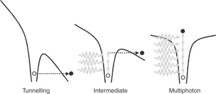
The degree to which MPA and electron tunnelling contributes to a photoionization event can be quantified using the Keldysh parameter (Keldysh, 1965):

where n is the refractive index, m* is the effective mass of the electron–hole pair, Eg is the energy band gap of the material and I and ω are the irradiance and angular frequency of the optical field respectively. The regime is said to be MPI if γ > 2, TI if γ < 0.5 and intermediate otherwise, although these delineation points are somewhat arbitrary and vary between authors. Inspection of Eq. [10.1] reveals that MPI is more predominant at lower irradiances, while TI is more predominant at higher irradiances. For a wide bandgap material (~5 eV) at a wavelength of 800 nm, the MPI regime corresponds to irradiances around 10 TW/cm2 or less, while the TI regime corresponds to irradiances around 100 TW/cm2 or greater.
10.2.4 Avalanche ionization
Free carriers generated through photo-ionization will continue to interact with optical fields, acquiring energy through inverse Bremsstrahlung absorption. Once a free carrier becomes energized it can transfer this energy to other electrons through collisions, liberating them and resulting in the formation of more free carriers (Wright, 1964). This form of ionization is termed impact ionization, also referred to as avalanche ionization as the growth of free carriers becomes exponential with time when this ionization mechanism dominates. Avalanche ionization is termed a secondary ionization process as it requires a population of free carriers (generated via photo-ionization for example) to seed the exponential growth. The large amount of absorbed energy associated with the rapid buildup of free carriers usually results in destruction of the substrate, thus avalanche ionization is typically associated with material damage. Avalanche ionization dominates when laser pulses are of the order of 1 ps or more. Ultrafast lasers with pulse durations of 250 fs or less are employed to achieve energy deposition within a bulk substrate without the destructive buildup of energy that occurs for longer pulse durations. Modifying a substrate without causing wholesale damage is the key to fabricating photonic components using the laser direct-write platform.
10.2.5 Self-focusing, plasma defocusing and fomentation
As a result of high incident irradiance, a host of other nonlinear mechanisms accompany ionization processes in a transparent medium. The most significant of these, from a laser machining point of view, are self-focusing and plasma defocusing, as these mechanisms result in significant distortion of the laser beam.
Self-focusing
The refractive index in an intense optical field is given as
where the function I(r, t) describes the spatiotemporal irradiance profile of the optical field (Chiao et al., 1964). The coefficient n2 is the nonlinear Kerr index and is related to the third-order nonlinear susceptibility,
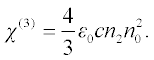
Irradiance profiles that are higher at the centre of the beam and fall away off axis induce a curvature in the wavefront similar to that induced by a lens. If n2 is positive (which is usually the case) this effect mimics that of a focusing lens. If the self-focusing effect is sufficiently strong, then the beam profile becomes increasingly more focused until the beam collapses in on itself. This power, beyond which occurs beam collapse, is called the critical power,

where α is a constant related to the beam profile (α = 3.77 for a Gaussian beam for example). In practice, beam collapse is arrested by other nonlinear mechanisms, including plasma defocusing.
Plasma defocusing
The presence of free carriers results in a local reduction in the refractive index,

where ρ is the plasma density (Feit and Fleck, 1974). By the same argument used above, this results in a curvature of the wavefront that has a defocusing effect on the beam. The interplay between self-focusing and plasma defocusing leads to laser pulses exhibiting complex behaviour as they propagate. This complex behaviour tends to be more prevalent when low (< 0.4) numerical aperture (NA) lenses are used to focus the laser beam.
Filamentation
One example of such complex behaviour is filamentation (Couairon and Mysyrowicz, 2007). Under certain conditions, the beam can repeatedly cycle between collapse due to self-focusing and plasma defocusing arresting the collapse. This continuing cycle of focusing and defocusing causes the beam to remain confined over long distances, a ‘filament’, rather than a beam that spreads out as it propagates. Filamentation cannot be sustained indefinitely as the energy of the beam is continually being depleted through plasma generation. Eventually the irradiance of the beam is not sufficient for self-focusing to overcome diffraction, at which point the beam ceases to propagate as a filament. It is possible for a beam to break up into multiple filaments, this can occur deterministically due to some form of anisotropy being present in either the beam or substrate, or stochastically due to fluctuations (noise) in the irradiance profile.
10.2.6 Ultrafast laser-induced modification
The formation of a plasma inside a dielectric leads to a cascade of physical processes that can result in a permanent local modification of the solid-state structure (Gattass and Mazur, 2008). Free carriers have a lifetime of the order of 1–10 ps, after which they begin to decay. When the plasma decays the energy of the free carriers is transferred to the phonon modes of the substrate, causing it to heat. If there is sufficient energy, the substrate undergoes localized softening and melting. Shock waves form during heating, dissipating energy away from the heated volume. The remaining energy is eventually lost through thermal diffusion. Since the heated volume is typically of the order of several μm3, the subsequent cooling is rapid, of the order of 1 μs or so. Rapid cooling means that structural changes that occur during heating become ‘frozen in’ which can result in a host of structural modifications including densification, rarefaction, devitrification, amorphization and colour centre formation. The change in refractive index that occurs in conjunction with these structural changes is particularly useful in photonics.
10.2.7 Cumulative heating
For ultrafast lasers with a sufficiently high pulse repetition rate (> 500 kHz), the deposited energy cannot fully dissipate away from the heated volume before the arrival of the next pulse. This results in thermal energy accumulating over many pulses, until thermal equilibrium is reached (Eaton et al., 2005). In this ‘cumulative heating’ regime, the nature of the ultrafast laser-induced modification depends on inter-pulse characteristics as well as properties of individual pulses. The advantage of the cumulative heating regime is the natural symmetry that modifications possess, as well as the rapid speed with which they can be written. There are some drawbacks to using this regime; most notably not all materials are suited for it (e.g. fused silica).
10.3 Refractive index modification mechanisms
On an atomic level, the refractive index of a medium is directly related to its polarizability, the dipole moment obtained per unit of applied electric field strength, per unit volume. Polarizability can be related to the refractive index via the Lorentz–Lorenz equation,

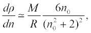
where α is the mean polarizability, ρ is the density, M is the molar mass and R is the molar refractivity. Changes to the refractive index of a material can therefore be related to a change in either ρ, R or M.
10.3.1 Densification and rarefaction
Densification and rarefaction can occur as a result of thermally induced volumetric changes that are ‘frozen in’ as a result of rapid cooling or mechanically induced volumetric changes due to the formation of shock waves or voids. From the Lorentz–Lorenz equation (Eq. [10.6]) an increase in density will result in an increase in the refractive index and vice versa. For small refractive index changes (< 1 × 10⁻²) the density is approximately proportional to the refractive index
where n0 is the unmodified refractive index. Conservation of mass dictates that densification must be accompanied by rarefaction, thus regions of positive refractive index change must accompany regions of negative refractive change where density change is the only refractive index change mechanism present.
10.3.2 Phase changes
Phase changes in this context refer to a material switching between crystalline states, or from a crystalline to amorphous state (or vice versa). The bonding arrangement of a given composition of atoms varies substantially between amorphous and various crystalline forms, for example, fused silica, α-quartz and β-quartz. This usually brings about a change in density, which will contribute to a modification in the refractive index; however, there is an additional contribution brought about by the change in the bond structure of the material (Little et al., 2010a). The effect of bond structure in the Lorentz–Lorenz equation is encapsulated by a change in the molar refractivity, R. Birefringence can also be induced or removed via phase changes through transitions between anisotropic and isotropic states.
10.3.3 Colour centres
Colour centres are defects within the bond structure of a material. They can manifest as atoms with incomplete octets (holes), electrons ‘stuck’ in excited states (excitons), missing atoms (vacancies), impurities (substitutions) or a combination of these. Colour centres are localized points in the material where the bond structure has been altered. The formation of colour centres therefore changes the molar refractivity of a material, independent of density change.
Colour centres have been shown to accompany ultrafast laser-induced modifications in the non-cumulative heating regime, and are thought to arise as a result of free electrons decaying into trapped excited (defect) states rather than the valence band. More recently, it has been suggested that colour centres also arise due to the breaking of bonds within the material (Fig. 10.2), or alternatively, the inability for bonds to reform after cooling (Little et al., 2010a). Colour centres are typically not photo-stable, meaning exposure to UV/visible wavelengths can result in the colour centres being removed (or photo-bleached) and the accompanying refractive index change washed out.
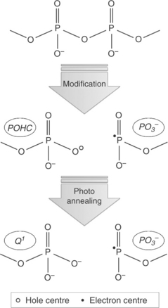
10.2 Colour centre formation/removal in phosphate glass under kHz repetition rates. Phosphorous–oxygen hole centres (POHCs) and PO3- ions form as a result of P–O bonds being broken during the modification process, and the subsequent removal of POHCs give rise to the increased proportion of P-tetrahedra bonded to a single bridging oxygen (Q1 P-tetrahedra).
When colour centres are removed in glass, it has been observed that only part of the accompanying refractive index change is erased (Dekker et al., 2010). This indicates that the glass does not revert back to its unmodified form after colour centres have been removed. By extension, changes in the bond structure of the glass that do not consist of colour centres must contribute to the refractive index change. The conversion of bridging oxygen atoms to non-bridging oxygen atoms was recently identified as a contributor of this type (Little et al., 2010b).
10.3.4 Stress
The application of compressive stress in a material can also result in a change in the refractive index. There is an isotropic contribution due to density changes that accompany mechanical compression, and an anisotropic component due to the stress itself. In crystalline media, it is generally difficult to induce a positive change in the refractive index directly, instead lines of negative refractive index change or even voids are written parallel to one another (Thomas et al., 2007). The space in between the voids is subject to compressive stress, which can act as the core of a waveguide. As the stress is anisotropic, it tends to induce birefringence, so waveguides of this type are often polarization-selective.
10.3.5 Voids
If the density of a plasma generated within a medium becomes sufficiently high then the Coulombic repulsion between particles results in a micro-explosion, forming a void (Glezer and Mazur, 1997). Voids are localized points of material damage consisting of vacuum pockets surrounded by a densified shell. The refractive index contrast that occurs as a result of void formation is (n – 1) ≈ 0.5, which is very large in comparison to other refractive index change mechanisms. Voids can be written with a great degree of repeatability and precision, making them useful for applications that make use of strong scattering centres in a precise formation, such as optical data storage and recovery (Glezer et al., 1996), and photonic crystals (Juodkazis et al., 2002).
Void formation is also the basis for writing point-by-point Bragg gratings in optical fibres with femtosecond laser pulses. This method has proven advantageous when writing Bragg gratings in active fibres as they can be inscribed in non-photosensitive media and do not degrade under high-power operation. In addition, voids can be anisotropic which allows the polarization of a fibre laser output to be manipulated (Jovanovic et al., 2009).
10.3.6 Nanostructure in fused silica
Focusing femtosecond pulses into fused silica can result in a quasi-periodic modification where the orientation of periods depends on the polarization of the femtosecond laser pulses. These types of modifications are termed nanostructures, or nanogratings, as the period of the modulation can be as small as 20 nm. It is not yet understood why this modification appears to be unique to fused silica and the mechanism by which these structures appear is still under debate. Pattathil et al. (2005) proposed that the quasi-periodic modulation arises as a result of the field enhancement around an initial ‘seed’ defect which in turn causes nanogratings to grow in a self-organized fashion. Shimotsuma et al. (2005) proposed an alternative explanation where the quasi-periodic modulation arises as a result of interference between waves excited within the electron plasma and the laser pulse.
Nanostructure formation is thought to be the underlying reason why modified glass regions experience an enhanced etch rate when exposed to hydrofluoric (HF) acid, and why the etch rate can be increased by a factor of 100 by varying the polarization of the femtosecond pulses (Hnatovsky et al., 2005). Modifying fused silica in this fashion is advantageous for fabricating microfluidic channels.
10.4 Photonic device processing
10.4.1 Device fabrication: experimental components and procedures
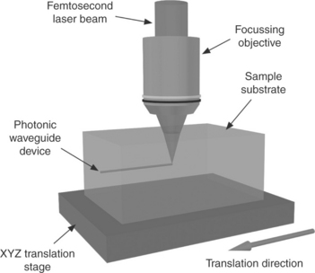
Figure 10.3 illustrates a typical femtosecond laser direct-write setup used for fabricating photonic devices inside bulk materials. The most common femtosecond laser systems used in this field are:
(i) regeneratively amplified Ti: Sapphire laser systems that provide high pulse energies (μJ–mJ) at kHz repetition rates
(ii) oscillator-only Ti:Sapphire systems with low energy (nJ) and high repetition rates (MHz)
(iii) high pulse energy (500 nJ–μJ) ytterbium or erbium-doped fibre lasers at high repetition rates (100 kHz–MHz)
(iv) low energy (nJ) cavity dumped ytterbium or Ti:Sapphire laser oscillators operating at high repetition rates (500 kHz–MHz).
As mentioned in the previous section, whilst all of these systems are effective at modifying transparent dielectrics, significant differences exist between the mechanism underlying the modification, and therefore, also the strength of the modification, level of damage (if any), and most importantly in terms of waveguides, whether the index change is positive or negative.
Femtosecond laser writing is achieved by focusing the laser beam from one of these systems (which can range from 780 nm up to 1560 nm, or include one of its harmonics) into a bulk sample using either a fixed microscope objective or lens. The sample to be processed is typically mounted on high precision motion controlled stages which are translated (by computer-linked drive control units) with respect to the laser beam to create (directly write) continuous structures in the bulk of the sample.
Optical head considerations
Most fabricators of photonic devices use microscope objectives rather than lenses given that they are well corrected with higher numerical aperture (NA). A variety of objectives with different NA and working distances have been used by researchers in the field allowing the size and shape of the fabricated structures to be tailored to a certain degree. Usually high numerical aperture (NA) objectives (typically > 0.6) are used in conjunction with high repetition rate systems as a tight focus is required in order to achieve sufficient intensities to modify the sample substrate. Such a tight focus is not required when using low repetition rate systems and lower NA objectives are typically used in those cases.
In practice, the higher the magnification the higher the fluence at focus and the smaller the working distance. Hence there is a trade-off that must be considered when selecting an objective to fabricate a specific device. The shorter the objective’s working distance the closer the focal point is to the surface of the glass sample. If the focal point gets too close to the surface, damage to the sample can arise and the capability to fabricate true 3D devices is reduced. The use of lower NA objectives requires higher writing powers to induce modification, which causes issues with self-focusing distorting the beam. Furthermore, employing low NA objectives produces challenges in achieving circularly symmetric local area index changes in bulk materials because the depth of field of the focal spot in these cases is larger than the lateral dimensions. In these cases simple beam-shaping techniques including asymmetric focusing using a slit aperture (Ams et al., 2005) or two-dimensional deformable mirror (Thomson et al., 2008), astigmatic cylindrical telescope arrangements (Cerullo et al., 2002), the multiscan method (Liu et al., 2004) or adaptive wavefront control using spatial light modulators (Mauclair et al., 2008) can recover this symmetry. Such techniques thus enable photonic devices with circular symmetry to be written using low magnification and long working distance objectives.
In the case of directly written photonic devices created below the surface of a substrate it is important to also consider the effect of spherical aberration that subsurface focusing causes. Spherical aberration and its effect on waveguide cross-sections can be controlled using objectives that are corrected for focusing through a fixed depth of material (for example, a cover slip corrected objective); however, this limits the 3D capabilities of the writing platform. A more suitable solution is to use oil-immersion focusing objectives that are not sensitive to the depth of focus in the material, since all optical path lengths to the focus remain constant, or to use adaptive optics techniques that compensate for the change in phase a wavefront experiences inside the material before the focal point (Jesacher and Booth, 2010).
Material and laser fabrication parameters
The material’s interaction processes at play within the laser focus are strongly dependent on both the material and the laser parameters, and it is common to observe both positive and negative changes in the material’s refractive index under different laser processing conditions or even within the same interaction region.
In most optical materials, the maximum refractive index change that can be induced using the direct-write technique is limited by material damage. At the other extreme, the minimum intensity that results in refractive index change depends on the material’s modification threshold, which in turn depends on nonlinear absorption coefficients and ionization cross-sections. The pulse energy required will depend on both the material and the chosen application. Different pulse energies will result in different peak index changes and associated variations in the guided mode field diameter (MFD) of resulting photonic devices. For example, certain phosphate glasses can display an interesting property in that not just the magnitude but also the sign of the net refractive index change induced by the writing laser is a function of pulse energy (Ams et al., 2008).
When using high repetition rate femtosecond laser systems, hundreds of pulses accumulate to heat the focal volume constituting an approximate point source of heat within the bulk of the material. Longer exposure of the material to this heat source gives rise to higher temperatures resulting in a larger affected region. Due to symmetric thermal diffusion outside of the focal volume, a spherically shaped modified region is produced. In contrast, when using a low repetition rate femtosecond laser system, the focal volume returns to room temperature before the arrival of the next pulse resulting in the same region of the material being heated and cooled many times by successive pulses. This repetitive type of machining means that the structural modification of the material is confined to the focal volume alone. It has also been shown that the refractive index contrast of a modified region can be increased by overwriting a waveguide with more than one pass of a low repetition rate femtosecond laser beam in a multiple fabrication scan fashion (Hirao and Miura, 1998).
It has been demonstrated that, for non-cumulative heating regimes, the material change (and accompanying refractive index changes) induced by circularly polarized pulses is different to that induced by linearly polarized pulses (Little et al., 2008). It has been suggested that this effect is due to the photo-ionization cross-sections being different for circularly polarized and linearly polarized pulses and the scaling of the multiphoton order as the power of the writing beam is increased (Little et al., 2011).
Other parameters which affect the writing properties, and thus the resulting device, include the sample translation speed and direction, focused beam shape, M2 value, wavelength and pulse duration. Resulting devices are not only dependent on these fabrication parameters but are also heavily influenced by the properties of the actual material in which the device is to be created: for example, bandgap energy, whether the sample is crystalline or amorphous, thermal characteristics, variations of impurities and dopants, and fracture strength. Typically, the parameter windows are relatively small for high-quality results in any given application (Ams et al., 2008).
10.4.2 Characterization of fabricated devices
After fabrication, the input and output facets of the material are ground and polished to expose the photonic device because the direct-write process cannot easily access the final few microns of glass near the edge of the target substrate. Photonic waveguide devices are generally characterized in terms of their transmission and reflection data, near- and far-field mode distributions, insertion, coupling, propagation and polarization dependent losses, induced refractive index contrasts, and if applicable, device gain. General experimental setups used to take such measurements from a device under test (DUT) are shown in Fig. 10.4. Various light sources (free space, fibre coupled, swept or tunable) at a variety of wavelengths (application dependent) are used to probe fabricated devices. Optical spectrum analysers (OSAs), power meters and charge-coupled device (CCD) cameras are used to analyse device properties. If characterization fibres are used to either pump light into or collect light from a DUT, index matching gel/oil is generally inserted at the fibre-DUT interface to reduce losses.

10.4 Photonic device characterization. Typical experimental layouts used to take (a) transmission and reflection measurements and (b) near-field distributions. DUT – device under test.
Mode field diameter
Near-field distributions exiting a fabricated device (Fig. 10.4) give an indication of the type of guided modes that are present in the device plus provide a means to measure the MFD of a guided mode. The MFD is defined as the distance between the 1/e points of the amplitude profile or 1/e2 points of the power density profile. The MFD is not necessarily the same dimension as the core. This can clearly be seen in Fig. 10.5, for example, where the MFD is plotted with respect to a step-index waveguide’s core diameter for a number of refractive index contrasts. The NA and the MFD of a single mode waveguide are inversely proportional to each other. The smaller the MFD, the greater the maximum exit radiation angle. Therefore, the MFD has a strong influence on a waveguide’s bending sensitivity and coupling efficiency with other optical devices.

Refractive index measurements
Variants of Fig. 10.5 (modified for the wavelength and type of glass of interest) can be used to estimate the peak refractive index change between the bulk material and the waveguide structures written using the ultrafast laser direct-write technique. Another computational method which uses the nearfield distribution directly can also be used (Mansour and Caccavale, 1996). Refractive index profilometers and QPM software packages are the most common methods of generating refractive index profiles of directly written photonic devices.
Photonic devices fabricated using the femtosecond laser direct-write technique are very small, of the order of microns. In addition to these dimensions being impossible to visualize via the naked eye, the human eye also cannot resolve the small refractive index contrasts that constitute an optical waveguide device. Transverse and end-on images of fabricated devices are therefore taken with a phase contrast or differential interference contrast (DIC) microscope. From these images approximate waveguide dimensions are measured. DIC microscopy is a beam-shearing interference technique in which a reference beam is sheared by a minuscule amount resulting in the interference of two distinct wavefronts that reach the final image plane slightly out of phase with each other. Essentially, the technique produces an image that displays the gradient of optical paths for both high and low spatial frequencies present in the material, that is, refractive index contrasts.
Photonic device losses
The insertion loss (IL) of a fabricated device is taken to be the ratio of the measured transmitted powers with and without the DUT in the setup shown in Fig. 10.4a and includes coupling, propagation, Fresnel and absorption losses. Coupling losses are usually estimated using the mode matching coupling efficiency formula outlined by Marcuse (1972) while absorption losses are material-specific and can be measured using a spectrometer. Propagation loss can then be determined by either subtracting the coupling, Fresnel and absorption losses from the IL, using the standard cutback method, or by taking the difference between the IL in reflection when the collecting fibre in Fig. 10.4a is replaced with a highly reflecting mirror aligned square to the device’s output and the IL in transmission without the mirror.
Device gain
The setup shown in Fig. 10.4a is slightly modified for active waveguide characterization in that wavelength division multiplexers (WDMs) are inserted at the device’s outputs so that both a signal source and a pump source can co-propagate along the device in a bidirectional configuration as outlined by Ams et al. (2009b).
10.5 Photonic devices
The femtosecond laser direct-write technique could potentially provide reliable and cheap devices with the best mode match to optical fibres, and thus find increasing applications in astronomy, medicine, biophotonics and quantum information. In fact, using this technique, researchers have shown that it is possible to fabricate a range of photonic devices of arbitrary dimension and design inside many different kinds of transparent glasses, polymers and crystals. The most common device created is of course the fundamental optical waveguide. Other devices, most of which are also based on the principle of guided light waves, have been fabricated by many international research groups.
10.5.1 Passive devices
The femtosecond laser direct-write technique has already been used to fabricate waveguides, waveguide arrays, power splitters, couplers, Mach Zehnder interferometers, gratings, Bragg gratings, computer-generated holograms, optical storage devices, interconnects, sensors (temperature, vibration and refractive index) and quantum simulation circuits inside a large host of bulk materials (details pertaining to these devices can be found in the reference list of this chapter). Although this field is still in its infancy, compared to other well-established techniques (silicon, ion-based and photosensitivity technologies), researchers are now benchmarking ultrafast laser direct-written devices against those made by the standard methodologies and are demonstrating comparable performance.
As mentioned previously, either a positive or negative refractive index change can be induced in a sample by the ultrafast direct-write technique. Investigations into increasing this contrast have been explored with a maximum positive index change of 2.2 × 10⁻² being reported (Eaton et al., 2010). The fabrication of single mode devices is possible with propagation losses typically smaller than 0.4 dB/cm. These characteristics make ultrafast laser-written waveguides ideal for use in applications where standard single mode fibres are used. The optical vibration sensor fabricated by Kamata et al. (2005) is an example of this. The sensor consists of a single straight waveguide written across a series of three pieces of glass with the central glass piece mounted on a suspended beam. Displacement of the central piece is detected by optical fibres that are used to measure the change in optical transmission through the device making it sensitive to mechanical vibration and acceleration. The sensor has a linear response over the frequency range 20 Hz–2 kHz and can detect accelerations as small as 0.01 m/s2.
The technique is not limited to 1D linear structures. For example, 2D arrays of evanescently coupled waveguides have been used to tune the dispersion and diffraction of propagating light (Szameit and Nolte, 2010) and 2D directional couplers have been used in quantum simulation circuits (Marshall et al., 2009) and as wavelength dependent splitters (Chen et al., 2008). Other wavelength dependent structures have also been reported. High quality waveguide Bragg-gratings (WBGs) (Marshall et al., 2006; Zhang et al., 2007), cascaded WBGs (Zhang et al., 2006), chirped WBGs (Zhang and Herman, 2009) and coupled WBGs (Ha et al., 2011) have all been demonstrated (for an example see Fig. 10.6). Typical WBGs have a coupling coefficient of κ = 2.5 cm−1 with 3 dB bandwidths less than 300 pm. One of the real potentials of the ultrafast laser direct-write technique was first demonstrated when Nolte et al. (2003) reported a 3D splitter with almost equal splitting ratios at 1.05 μm. This paved the way for further 3D devices to be realized. For example, a 3D electro-optic subsurface modulator coupled to surface electrodes resulting in an integrated device with an effective electro-optic coefficient of 0.17 pm/V (Li et al., 2006) and the demonstration of 3D interconnections of silica-based planar lightwave circuit (PLC) waveguides using ultrafast laser-written waveguides (Nasu et al., 2009).

10.6 Example waveguide Bragg-grating (WBG) demonstrating the control of the ultrafast laser direct-write technique. (a) Schematic of a WBG fabricated using the modulated writing beam method. (b) Differential interference contrast (DIC) top-view micrograph of a WBG structure fabricated in a borosilicate glass sample clearly showing the 500 nm grating period. (c) C-band transmission and reflection spectra from the WBG.
10.5.2 Active devices
Active waveguide devices fabricated using the femtosecond laser direct-write technique have been reported in various materials: Nd-doped silicate glass, Er/Yb co-doped phosphate glass, LiF crystal, Nd-doped and Yb-doped YAG crystal, Er-doped bismuthate glass, Er-doped and Er/Yb co-doped oxyfluoride silicate glass, and Er-doped and Er/Yb co-doped phospho-tellurite glass. These samples were specifically chosen due to their target application, region of wavelength emission and ease of doping with rare-earth ions. Of these materials, the phosphate glass hosts are best suited to active device fabrication for use in telecommunications as tens of percent by weight of rare-earth ions can be held in solution offering the highest gain-per-unit length value (4 dB/cm) in the C-band without detrimental effects such as ion-clustering.
Waveguide amplifiers
Small signal gain characteristics of a waveguide written in a doped material are measured at the wavelength corresponding to the peak of the material’s gain curve. To date, internal gains of 3.18 dB/cm in the C-band have been reported for Er/Yb doped phosphate systems (Osellame et al., 2008) and a gain of 1.5 dB/cm at 1054 nm for a femtosecond laser-written waveguide amplifier fabricated in Nd-doped silicate glass (Sikorski et al., 2000). There is still potential for further improvement of the gain of these devices by optimizing the doping concentrations of the active ions, optimizing the waveguide amplifier length and optimizing pump power configurations. Furthermore, there is scope to develop glasses that are engineered for the direct-write process, as the doped glasses typically used are those developed for use in fibre preforms and ion exchange processes. An example of why this may be necessary is demonstrated by Dekker et al. (2010), who show that annealing of colour centres during characterization causes device degradation over time. It is worth noting, however, that the waveguide amplifiers reported to date created using the ultrafast laser direct-write technique (Ams et al., 2009b; Della Valle et al., 2009) have reached a performance level (net gain of 2.7 dB/cm) comparable to those demonstrated with conventional fabrication techniques (net gain of 3 dB/cm) in similar glasses with the same dopant concentrations (Jaouen et al., 1999, for example).
To turn these amplifiers into laser oscillators, appropriate feedback of the particular amplified frequency is required. Positive feedback may be obtained by placing the gain material between a pair of suitable mirrors which form an optical cavity or resonator. With guided wave devices, the cavity usually takes the form of a Distributed Bragg Reflector (DBR) geometry or a Distributed Feedback (DFB) design, although external dielectric mirrors or dichroic coatings on the amplifier’s end facets can also be used.
DBR waveguide oscillators
The laser cavity employed by some research groups in the field is formed by butt-coupling fibre Bragg gratings (FBGs) (which act as cavity mirrors) to the waveguide amplifier (Osellame et al., 2008; Psaila et al., 2008). The FBGs are centred at the same wavelength but have different reflectivities and bandwidth. This enables a laser cavity to be created with a high reflector at one end and an output coupler at the other. Such a cavity led to the demonstration of ultrafast laser-written waveguide lasers (WGLs) able to provide wavelength coverage over the entire C-band, single longitudinal mode and stable mode-locking operation. In particular, recent reports have indicated that using a cavity length of 5.5 cm and a 57% output coupler, a WGL with threshold pump power of 124 mW and slope efficiency of 21% is achievable. Furthermore, a mode-locked WGL source based on carbon nanotubes technology (used to create a saturable absorber) has been reported (Osellame et al., 2008). This WGL had a repetition rate of 16.7 MHz and pulse duration of 1.6 ps.
Integrated DFB waveguide oscillators
A serious handicap of the feedback provided by mirror resonators is that many longitudinal modes may fit under the system’s gain bandwidth thus impeding single longitudinal mode operation. In addition, the device is not completely monolithic. Several experimental techniques have been reported that enable the realization of Bragg grating structures inside femtosecond laser-written waveguides to create a cavity. Kawamura et al. (2004) developed a hologram technique to encode grating structures inside an LiF crystal by a single interfered femtosecond laser pulse. When side-pumping the grating with 450 nm light, a DFB laser oscillator at 707 nm was created. The grating structure, however, was weak and not permanent as the colour centres creating it were eliminated by annealing.
More recently, by square-wave modulating a low repetition rate femtosecond laser’s output, in a fashion reported by Zhang et al. (2007), first order permanent waveguide Bragg gratings (WBGs) were directly written inside Er/Yb co-doped and Yb-doped phosphate glasses in a single fabrication step (Ams et al., 2009a; Marshall et al., 2008). A waveguide variant of a distributed feedback (DFB) laser was hence demonstrated (Fig. 10.7). The total output power of these lasers measured 0.37 mW at 1535 nm and 102 mW at 1032 nm respectively with linewidths less than 4 pm and efficiencies up to 17%. Although it is known that the WBG structure contributes to an increase in the propagation loss of the amplifier device (Zhang et al., 2007), clearly the WBG is of a high enough quality that the internal gain in the system still exceeds this increase.

10.7 Example distributed feedback (DFB) waveguide laser (WGL) at 1032 nm fabricated in a 9% ytterbium (Yb) doped phosphate glass sample. The top image shows the cooperative luminescence along the device while pumping at 976 nm. The bottom spectrum plots the laser output power of the 9.5 mm long WGL as a function of pump power. The inset shows the output spectrum of the WGL at 102 mW output power with the ordinate axis scale referenced to the peak.
Other waveguide oscillators
A near Gaussian mode WGL at 1064 nm was realized in an Nd-doped YAG crystal by writing parallel damage tracks in the crystalline lattice (Siebenmorgen et al., 2009). Waveguiding was observed in the unmodified region between the pair of tracks due to stress-induced birefringence of the material. Laser operation was achieved without the use of external mirrors but by using only the Fresnel reflection of about 9% at the device end facets. Pumping the device with a continuous wave 808 nm Ti:Sapphire laser resulted in an output power of 25.5 mW and a power conversion efficiency of 23%. By using the same techniques, Siebenmorgen et al. (2010) also demonstrated waveguide laser action at 1030 nm in a Yb-doped YAG crystal. An output power of 0.8 W with 1.2 W of launched pump power was achieved, resulting in a record WGL slope efficiency of 75%.
Very recently a Tm3+ doped ZBLAN glass WGL was reported which produced 47 mW at 1880 nm (Lancaster et al., 2011). This is the first report of a mid-IR WGL fabricated using the femtosecond laser direct-write technique. The waveguide cladding was defined by two overlapped rings made up of directly written modified glass tubes, resulting in a depressed-index cladding structure. The laser resonator was created using external dielectric mirrors resulting in a 50% internal slope efficiency and a measured M2 value of 1.7.
10.5.3 Hybrid devices
Microfluidics is the science and technology of systems that process or manipulate small amounts of liquids using channels with dimensions of tens to hundreds of micrometres. Introduction of photonic technologies into these systems created the field of optofluidics and developed an analytical tool capable of gleaning information such as the size, shape, concentration, chemical composition and structural organization of liquid-borne particles. Many comprehensive articles are available on the applications and current state-of-the-art of the optofluidics discipline (Hunt and Wilkinson, 2008; Monat et al., 2007).
A key advantage of the femtosecond laser direct-write technique is that the laser exposed regions of the material may be preferentially removed using an acid etchant (typically hydrofluoric [HF] acid) to create hollow channels and thus microfluidic pathways (Marcinkevicius et al., 2001). Hence, the femtosecond laser direct-write technique is a powerful tool offering a single laser system which can be used to create both microphotonic and microfluidic devices inside the same glass sample with the opportunity to also integrate these devices in 3D. A handful of groups in the world have this capability and are beginning to make simple integrated optofluidic modules (Osellame et al., 2007). In addition, there is commercial interest in this technology with Translume Inc. now offering microfluidic devices fabricated in fused silica glass for purchase.
10.6 Conclusions
The femtosecond laser direct-write technique is a technology capable of producing high-quality integrated photonic devices inside bulk transparent materials without the need for lithography, etching, a controlled environment or much sample preparation. The nonlinear ionization processes that underpin light–matter interactions and the means by which local refractive index changes are resultant were reviewed. Densification and rarefaction (of which void formation is an extreme example) were identified as primary contributors. Phase changes and colour centres could also contribute, due to the change in local bond structure (molar refractivity) and the consequent change in the polarizability they impart; even in the absence of density changes. The typical experimental methods for utilizing these processes to fabricate and characterize subsurface photonic waveguide devices were presented. Photonic devices fabricated in both passive and active glasses were briefly discussed with particular attention being directed to the fabrication of all-optical waveguide amplifiers and monolithic laser oscillators. The comparable performance of ultrafast laser-written devices with devices fabricated using traditional methods has generated a lot of interest in a variety of research fields. Biologists, astronomers, quantum physicists and engineers alike are already harnessing the capabilities of the femtosecond laser direct-write technique, and with breakthrough scientific fields continuing to emerge it appears that this trend will continue.
10.7 References
Ams, M., Dekker, P., Marshall, G.D., Withford, M.J. Monolithic 100 mW Yb waveguide laser fabricated using the femtosecond-laser direct-write technique. Optics Letters. 2009; 34:247–249.
Ams, M., Marshall, G.D., Dekker, P., Dubov, M., Mezentsev, V.K., Bennion, I., Withford, M.J. Investigation of ultrafast laser–photonic material interactions: Challenges for directly written glass photonics. IEEE Journal of Selected Topics in Quantum Electronics. 2008; 14:1370–1381.
Ams, M., Marshall, G.D., Dekker, P., Piper, J.A., Withford, M.J. Ultrafast laser written active devices. Laser & Photonics Review. 2009; 3:535–544.
Ams, M., Marshall, G.D., Spence, D.J., Withford, M.J. Slit beam shaping method for femtosecond laser direct-write fabrication of symmetric waveguides in bulk glasses. Optics Express. 2005; 13:5676–5681.
Apostolopoulos, V., Laversenne, L., Colomb, T., Depeursinge, C., Salathe, R.P., Pollnau, M., Osellame, R., Cerullo, G., Laporta, P. Femtosecond-irradiation-induced refractive-index changes and channel waveguiding in bulk Ti$^{3+}$: Sapphire. Applied Physics Letters. 2004; 85:1122–1124.
Cerullo, G., Osellame, R., Taccheo, S., Marangoni, M., Polli, D., Ramponi, R., Laporta, P., De Silvestri, S. Femtosecond micromachining of symmetric waveguides at 1.5 $mu$m by astigmatic beam focusing. Optics Letters. 2002; 27:1938–1940.
Chen, W.-J., Eaton, S.M., Zhang, H., Herman, P.R. Broadband directional couplers fabricated in bulk glass with high repetition rate femtosecond laser pulses. Optics Express. 2008; 16:11470–11480.
Chiao, R.Y., Garmire, E., Townes, C.H. Self-trapping of optical beams. Physical Review Letters. 1964; 13:479–482.
Couairon, A., Mysyrowicz, A. Femtosecond filamentation in transparent media. Physics Reports: Review Section of Physics Letters. 2007; 441:47–189.
Davis, K.M., Miura, K., Sugimoto, N., Hirao, K. Writing waveguides in glass with a femtosecond laser. Optics Letters. 1996; 21:1729–1731.
Dekker, P., Ams, M., Marshall, G.D., Little, D.J., Withford, M.J. Annealing dynamics of waveguide Bragg gratings: evidence of femtosecond laser induced colour centres. Optics Express. 2010; 18:3274–3283.
Della Valle, G., Osellame, R., Laporta, P. Micromachining of photonic devices by femtosecond laser pulses. Journal of Optics A: Pure and Applied Optics. 2009; 11:013001.
Eaton, S.M., Ng, M.L., Osellame, R., Herman, P.R. High refractive index contrast in fused silica waveguides by tightly focused, high-repetition rate femtosecond laser. Journal of Non-Crystalline Solids. 2010; 357:2387–2391.
Eaton, S.M., Zhang, H.B., Herman, P.R. Heat accumulation effects in femtosecond laser-written waveguides with variable repetition rate. Optics Express. 2005; 13:4708–4716.
Feit, M.D., Fleck, J.A. Effect of refraction on spot-size dependence of laser-induced breakdown. Applied Physics Letters. 1974; 24:169–172.
Gattass, R.R., Mazur, E. Femtosecond laser micromachining in transparent materials. Nature Photonics. 2008; 2:219–225.
Glezer, E.N., Mazur, E. Ultrafast-laser driven micro-explosions in transparent materials. Applied Physics Letters. 1997; 71:882–884.
Glezer, E.N., Milosavljevic, M., Huang, L., Finlay, R.J., Her, T.H., Callan, J.P., Mazur, E. Three-dimensional optical storage inside transparent materials. Optics Letters. 1996; 21:2023–2025.
Göppert-Mayer, M. Über Elementarakte mit zwei Quantensprüngen. Annalen der Physik Berlin. 1931; 401:273–294.
Ha, S., Ams, M., Marshall, G.D., Neshev, D.N., Sukhorukov, A.A., Kivshar, Y.S., Withford, M.J. Control of light transmission in laser-written phase-shifted Bragg grating couplers. Optics Letters. 2011; 36:1380–1382.
Hirao, K., Miura, K. Writing waveguides and gratings in silica and related materials by a femtosecond laser. Journal of Non-Crystalline Solids. 1998; 239:91–95.
Hnatovsky, C., Taylor, R.S., Simova, E., Bhardwaj, V.R., Rayner, D.M., Corkum, P.B. Polarization-selective etching in femtosecond laser-assisted microfluidic channel fabrication in fused silica. Optics Letters. 2005; 30:1867–1869.
Hunt, H.C., Wilkinson, J.S. Optofluidic integration for microanalysis. Microfluidics and Nanofluidics. 2008; 4:53–79.
Jaouen, Y., Du Mouza, L., Barbier, D., Delavaux, J.M., Bruno, P. Eight-wavelength Er-Yb doped amplifier: Combiner/splitter planar integrated module. Photonics Technology Letters, IEEE. 1999; 11:1105–1107.
Jesacher, A., Booth, M.J. Parallel direct laser writing in three dimensions with spatially dependent aberration correction. Optics Express. 2010; 18:21090–21099.
Jovanovic, N., Thomas, J., Williams, R.J., Steel, M.J., Marshall, G.D., Fuerbach, A., Nolte, S., Tunnermann, A., Withford, M.J. Polarization-dependent effects in point-by-point fiber Bragg gratings enable simple, linearly polarized fiber lasers. Optics Express. 2009; 17:6082–6095.
Juodkazis, S., Matsuo, S., Misawa, H., Mizeikis, V., Marcinkevicius, A., Sun, H.B., Tokuda, Y., Takahashi, M., Yoko, T., Nishii, J. Application of femtosecond laser pulses for microfabrication of transparent media. Applied Surface Science. 2002; 197:705–709.
Kamata, M., Obara, M., Gattass, R.R., Cerami, L.R., Mazur, E. Optical vibration sensor fabricated by femtosecond laser micromachining. Applied Physics Letters. 2005; 87:051106.
Kawamura, K., Hirano, M., Kurobori, T., Takamizu, D., Kamiya, T., Hosono, H. Femtosecond-laser-encoded distributed-feedback color center laser in lithium fluoride single crystals. Applied Physics Letters. 2004; 84:311–313.
Keldysh, L.V. Ionization in the field of a strong electromagnetic wave. Soviet Physics JETP. 1965; 20:1307–1314.
Lancaster, D.G., Gross, S., Ebendorff-Heidepriem, H., Kuan, K., Monro, T.M., Ams, M., Fuerbach, A., Withford, M.J. Fifty percent internal slope efficiency femtosecond direct-written Tm3+:ZBLAN waveguide laser. Optics Letters. 2011; 36:1587–1589.
Li, G.Y., Winick, K.A., Said, A.A., Dugan, M., Bado, P. Waveguide electrooptic modulator in fused silica fabricated by femtosecond laser direct writing and thermal poling. Optics Letters. 2006; 31:739–741.
Little, D.J., Ams, M., Dekker, P., Marshall, G.D., Dawes, J.M., Withford, M.J. Femtosecond laser modification of fused silica: The effect of writing polarization on Si-O ring structure. Optics Express. 2008; 16:20029–20037.
Little, D.J., Ams, M., Dekker, P., Marshall, G.D., Withford, M.J. Mechanism of femtosecond-laser induced refractive index change in phosphate glass under a low repetition-rate regime. Journal of Applied Physics. 2010; 108:033110–033115.
Little, D.J., Ams, M., Gross, S., Dekker, P., Miese, C.T., Fuerbach, A., Withford, M.J. Structural changes in BK7 glass upon exposure to femtosecond laser pulses. Journal of Raman Spectroscopy. 2010; 42:715–718.
Little, D.J., Ams, M., Withford, M.J. Influence of bandgap and polarization on photo-ionization: Guidelines for ultrafast laser inscription [Invited]. Optical Materials Express. 2011; 1:670–677.
Liu, J.R., Zhang, Z.Y., Flueraru, C., Liu, X.P., Chang, S.D., Grover, C.P. Waveguide shaping and writing in fused silica using a femtosecond laser. IEEE Journal of Selected Topics in Quantum Electronics. 2004; 10:169–173.
Mansour, I., Caccavale, F. An improved procedure to calculate the refractive index profile from the measured near-field intensity. Journal of Lightwave Technology. 1996; 14:423–428.
Marcinkevicius, A., Juodkazis, S., Watanabe, M., Miwa, M., Matsuo, S., Misawa, H., Nishii, J. Femtosecond laser-assisted three-dimensional microfabrication in silica. Optics Letters. 2001; 26:277–279.
Marcuse, D.Light transmission optics. New York: Van Nostrand Reinhold Company, 1972.
Marshall, G.D., Ams, M., Withford, M.J. Direct laser written waveguide-Bragg gratings in bulk fused silica. Optics Letters. 2006; 31:2690–2691.
Marshall, G.D., Dekker, P., Ams, M., Piper, J.A., Withford, M.J. Directly written monolithic waveguide laser incorporating a distributed feedback waveguide-Bragg grating. Optics Letters. 2008; 33:956–958.
Marshall, G.D., Politi, A., Matthews, J.C.F., Dekker, P., Ams, M., Withford, M.J., O’Brien, J.L. Laser written waveguide photonic quantum circuits. Optics Express. 2009; 17:12546–12554.
Martinez, A., Khrushchev, I.Y., Bennion, I. Thermal properties of fibre Bragg gratings inscribed point-by-point by infrared femtosecond laser. Electronics Letters. 2005; 41:176–178.
Mauclair, C., Mermillod-Blondin, A., Huot, N., Audouard, E., Stoian, R. Ultrafast laser writing of homogeneous longitudinal waveguides in glasses using dynamic wavefront correction. Optics Express. 2008; 16:5481–5492.
Monat, C., Domachuk, P., Eggleton, B.J. Integrated optofluidics: A new river of light. Nature Photonics. 2007; 1:106–114.
Nasu, Y., Kohtoku, M., Hibino, Y., Inoue, Y. Waveguide interconnection in silica-based planar lightwave circuit using femtosecond laser. Journal of Lightwave Technology. 2009; 27:4033–4039.
Nolte, S., Will, M., Burghoff, J., Tunnermann, A. Femtosecond waveguide writing: a new avenue to three-dimensional integrated optics. Applied Physics A: Materials Science and Processing. 2003; 77:109–111.
Okhrimchuk, A.G., Shestakov, A.V., Khrushchev, I., Mitchell, J. Depressed cladding, buried waveguide laser formed in a YAG:Nd3+ crystal by femtosecond laser writing. Optics Letters. 2005; 30:2248–2250.
Osellame, R., Della Valle, G., Chiodo, N., Taccheo, S., Laporta, P., Svelto, O., Cerullo, G. Lasing in femtosecond laser written optical waveguides. Applied Physics A: Materials Science and Processing. 2008; 93:17–26.
Osellame, R., Maselli, V., Vazquez, R.M., Ramponi, R., Cerullo, G. Integration of optical waveguides and microfluidic channels both fabricated by femtosecond laser irradiation. Applied Physics Letters. 2007; 90:231118.
Pattathil, R.P., Hnatovsky, C., Bjardwaj, V.R., Simova, E., Taylor, R.S., Rayner, D.M., Corkum, P.B. Femtosecond laser-induced nanostructures in fused silica. Proceedings of SPIE. 2005; 5971:59711D.
Psaila, N.D., Thomson, R.R., Bookey, H.T., Chiodo, N., Shen, S., Osellame, R., Cerullo, G., Jha, A., Kar, A. Er:Yb-doped oxyfluoride silicate glass waveguide laser fabricated using ultrafast laser inscription. IEEE Photonics Technology Letters. 2008; 20:126–128.
Shimotsuma, Y., Hirao, K., Qiu, J.R., Kazansky, P.G. Nano-modification inside transparent materials by femtosecond laser single beam. Modern Physics Letters B. 2005; 19:225–238.
Siebenmorgen, J., Calmano, T., Petermann, K., Huber, G. Highly efficient Yb:YAG channel waveguide laser written with a femtosecond-laser. Optics Express. 2010; 18:16035–16041.
Siebenmorgen, J., Petermann, K., Huber, G., Rademaker, K., Nolte, S., Tünnermann, A. Femtosecond laser written stress-induced Nd:Y3Al5O12 (Nd:YAG) channel waveguide laser. Applied Physics B: Lasers and Optics. 2009; 97:251–255.
Sikorski, Y., Said, A.A., Bado, P., Maynard, R., Florea, C., Winick, K.A. Optical waveguide amplifier in Nd-doped glass written with near-IR femtosecond laser pulses. Electronics Letters. 2000; 36:226–227.
Szameit, A., Nolte, S. Discrete optics in femtosecond-laser-written photonic structures. Journal of Physics B: Atomic, Molecular and Optical Physics. 2010; 43:163001.
Thomas, J., Heinrich, M., Burghoff, J., Nolte, S., Ancona, A., Tunnermann, A. Femtosecond laser-written quasi-phase-matched waveguides in lithium niobate. Applied Physics Letters. 2007; 91:151108.
Thomas, J., Heinrich, M., Zeil, P., Hilbert, V., Rademaker, K., Riedel, R., Ringleb, S., Dubs, C., Ruske, J.-P., Nolte, S., Tünnermann, A. Laser direct writing: Enabling monolithic and hybrid integrated solutions on the lithium niobate platform. Physica Status Solidi (A). 2011; 208:276–283.
Thomson, R.R., Bockelt, A.S., Ramsay, E., Beecher, S., Greenaway, A.H., Kar, A.K., Reid, D.T. Shaping ultrafast laser inscribed optical waveguides using a deformable mirror. Optics Express. 2008; 16:12786–12793.
Wright, J.K. Theory of electrical breakdown of gases by intense pulses of light. Proceedings of the Physical Society. 1964; 84:41–46.
Zhang, H., Herman, P.R. Chirped Bragg grating waveguides directly written inside fused silica glass with an externally modulated ultrashort fiber laser. Photonics Technology Letters, IEEE. 2009; 21:277–279.
Zhang, H.B., Eaton, S.M., Herman, P.R. Single-step writing of Bragg grating waveguides in fused silica with an externally modulated femtosecond fiber laser. Optics Letters. 2007; 32:2559–2561.
Zhang, H.B., Eaton, S.M., Li, J.Z., Herman, P.R. Femtosecond laser direct writing of multiwavelength Bragg grating waveguides in glass. Optics Letters. 2006; 31:3495–3497.