
Laser-assisted polymer joining methods for photonic devices
Abstract:
This chapter presents the development of laser-based methods for assembly of photonic devices. This includes the development of laser-assisted polymer bonding methods for assembly and packaging of photonic and microelectromechanical systems (MEMS) devices and the associated temperature monitoring method using embedded microsensors. The chapter also covers an overview of the development of a laser microwelding method for assembly of polymer spheres to create photonic bandgap materials for terahertz applications.
8.1 Introduction
Microscale joining and bonding methods are essential for assembly and packaging of photonic devices and structures for a variety of applications such as coupling of optical fibres to lasers and integration of photonic devices with other microelectronic devices and microelectromechanical systems (MEMS). One well-established application of lasers in assembly of photonic devices is laser welding of metal clips to a metal ferrule on an optical fibre to produce a fibre-coupled semiconductor laser inside a butterfly package. Following the development of the laser welding technology in the 1990s (Jang, 1996), it has become a mature manufacturing method for high speed and high reliability assembly of fibre-coupled laser packages (Jang, 2000; Song et al., 2009; Tan et al., 2005). Lasers are efficient remote heat sources that can deliver a well-controlled beam to an area between parts or components to produce a reliable joint by welding or other thermally induced joining mechanisms. With the rapid development of high-power, high-efficiency diode laser technology and the diode laser pumped solid state lasers, lasers will find many other applications in assembly of photonic devices. This chapter is focused on development of laser-assisted polymer bonding of substrates for photonic and MEMS applications. One potential application of the technology is in encapsulation of photonic components such as lasers, optical detectors, imaging sensors and MEMS devices including optical MEMS. The method offers a potential solution to low cost, low temperature assembly and packaging requirements. The application of the bonding polymer, benzocyclobutene (BCB), in fabrication of semiconductor lasers as a dielectric material for planarization is also covered. The chapter also describes other emerging applications of lasers in assembly of photonic bandgap structures for terahertz applications.
8.2 Properties of benzocyclobutene (BCB) polymers for photonic applications
8.2.1 BCB polymer
BCB represents a family of thermosetting polymers developed by Dow Chemical for microelectronic and photonic applications. Table 8.1 shows a summary of the properties of the BCB polymers. The details of these and further information on the properties of the BCB polymers are available from the manufacturer (Dow Chemical, 2011). The low dielectric constant of the BCB polymers makes them a good dielectric material for fabrication of microelectronic circuits and photonic devices. Polymer materials with a low dielectric constant are essential for high frequency microelectronic and photonic systems. The BCB polymers have good thermal stability and low moisture uptake characteristics. High quality thin films can be produced easily by spin-coating. The BCB polymer films are prepared using B-staged monomer solutions. This means that the curing reaction is already initiated and ready for completion after a film is produced. This can enhance its viscosity stability (Wong, 2000). The photosensitive BCB materials can be patterned by UV lithography and therefore are compatible with the standard microfabrication methods. The photosensitive polymers contain diazo cross-linker moieties. The BCB polymers that are not photosensitive can be patterned using dry etching methods. Therefore the BCB polymers are versatile materials with processing flexibility.
Table 8.1
Summary of properties of BCB polymers
| Glass transition temperature | > 350°C |
| Coefficient of thermal expansion | 42 ppm/°C at 25°C |
| Thermal conductivity | 0.293 W/m/K at 24°C |
| Tensile modulus | 2.9 GPa |
| Volume resistivity | 1 × 10¹⁹ Ω cm |
| Dielectric constant | 2.5 at 10 GHz |
| Breakdown electric field | ~ 5.3 × 10⁶ V/cm |
| Refractive index | 1.56 at 633 nm |
| Moisture uptake | < 0.2% |
Source: Dow Chemical (2011).
8.2.2 Curing characteristics of BCB polymers
The BCB polymer is a thermal setting resin. It can be cured between 200°C and 350°C. However the curing behaviour is highly dependent on the curing temperature. Figure 8.1 shows the relationship between curing time and temperature for an oven-based curing method (Dow Chemical, 2009). It takes 60 min to achieve over 95% of curing (hard cure) at 250°C, but the curing time can be reduced to a few seconds at curing temperatures above 320°C. This unique property makes it possible to achieve a short processing time provided that a rapid heating method is used such as the laser-based assembly method described in this chapter.

8.1 Curing behaviour of BCB for an oven-based method. From Dow Chemical, 2009.
8.3 BCB as a planarization material for fabrication of semiconductor photonic devices
In fabrication of photonic devices such as semiconductor lasers, it is necessary to passivate the ridge waveguide structures to complete the fabrication process. The passivation layer surrounding the ridge waveguide structure is used to provide better confinement of the injected current for laser operation and to suppress the diffraction effects by improving index matching between the waveguide and the air interface. BCB has been used as a planarization material in fabrication of semiconductor lasers. In the work by Wiedmann et al. (2001) a BCB polymer was used as the planarization material to passivate InP-based III-V quantum well semiconductors. The active waveguide medium is deposited using an epitaxy method and carried out at wafer scale including additional layers for cladding and ohmic contact. A metal layer is deposited on top of the epitaxy layer for ohmic contact for producing electrodes for the resultant lasers. The multilayer stack is patterned using electron beam lithography and a combination of dry and wet etching methods to obtain freestanding structures including the distributed Bragg reflectors (DBR) to complete the laser fabrication process. A BCB layer is then coated on the etched structures by spin-coating to fill in the vertical gaps in the laser cavities and structures for the DBR reflector. After baking at 250°C for 2 h, the BCB material above the mesa structure is removed by reactive ion etching. Single mode operation of the lasers is achieved at 1.5 μm of wavelength using BCB as the dielectric material for planarization. BCB has been used in a similar manner for fabrication of a ridge waveguide laser operating at 1.3 μm (Yagi et al., 2009). An electrical bandwidth of more than 20 GHz is obtained as a result of reduction of the parasitic capacitance using the BCB buried ridge waveguide structure in the laser. Reliable operation of the laser is demonstrated in accelerated testing for 1200 h at 85°C of temperature and 200 mA of operating current.
In another application of BCB as a planarization polymer for fabrication of semiconductor photonic devices (Demir et al., 2005), a photonic switch is fabricated based on the integration of a mesa photodiode and a quantum well modulator on the same substrate. After selective deposition of the semiconductor layers, a silicon dioxide or silicon nitride based hard mask is produced on the wafer and used to define the areas for device fabrication. The exposed material is etched away vertically to the substrate surface. Selective removal of additional material under the hard mark is useful to create a small degree of undercut in order to produce an extended region of flat BCB surface beyond the ridge structures after the BCB based planarization process. The BCB layer is deposited using spin-coating after fabrication of the device structures under the hard mask. The BCB material seals the structures for photonic devices. After BCB curing the material is etched back to the surface of the hard mask. The advantage of the hard mask approach is that it allows easy control of the process since the hard mask acts as an etch stopper to prevent excessive etching of the BCB material for passivation of the detector and modulator. Using BCB as a planarization material, high yield (> 90%) fabrication, high breakdown voltage and low contact resistance can be achieved.
8.4 Laser-assisted polymer bonding for assembly of photonic and microelectromechanical systems (MEMS) devices
This section describes the development of laser-assisted polymer bonding methods for assembly and packaging of microelectronic, photonic and MEMS devices. An energy efficient diode laser is used to cure a patterned square BCB ring to obtain fast, reliable bonding of glass and silicon substrates for capping or substrate attachment in packaging and integration applications. An accurate temperature monitoring method for the laser bonding process using embedded microsensors has been developed.
8.4.1 Principle of laser-assisted polymer bonding
In the laser-based intermediate polymer layer substrate bonding method, a laser is used to cure a polymer adhesive layer to join two substrates together to form a substrate assembly as illustrated in Fig. 8.2 (Bardin et al., 2007). The laser radiation can be absorbed by one of the substrates or the polymer layer itself to produce the necessary temperature rise to cure the polymer layer to form a strong bond between the substrates. The intermediate layer polymer bonding method allows low temperature and low stress joining of substrates for assembly and packaging of photonic, MEMS and microelectronic devices. It is a flexible approach for bonding of a range of substrate materials for which direct interface bonding is not possible due to incompatibility of the surfaces or requiring extreme high temperature such as silicon direct bonding. Figure 8.3a shows a schematic arrangement for bonding a transparent substrate to a non-transparent substrate while Fig. 8.3b illustrates bonding of two non-transparent substrates. The substrate configuration in Fig. 8.3a can be reversed to have the non-transparent substrate facing the laser beam in the same approach as shown in Fig. 8.3b. A glass cap is commonly used for photonic and optical devices as well as optical MEMS such as micromirrors to provide a window for the input and output light beams. For encapsulation of other MEMS devices non-transparent caps are usually used to provide a perfect CTE (coefficient of thermal expansion) match between the substrates thus improving the thermomechanical reliability of the resultant package. For example, a silicon cap is preferred for silicon-based MEMS devices such as accelerometers, gyroscopes and resonators. Silicon is a non-transparent material for laser wavelengths below 1.1 μm.


8.4.2 Beam-forming method
In the laser-assisted polymer bonding method two beam delivery approaches can be used, one based on scanning a focused beam along the polymer bonding track and the second approach based on projection of a laser beam to cover the total area to be processed. When it is not possible to cover the entire bonding area, for example at wafer level processing, each area of the wafer can be processed using the beam project method in sequence to complete wafer level bonding. The beam projection approach is more efficient since an area is processed simultaneously rather than a spot as is the case in the scanning method. In order to make efficient use of laser output and to produce a uniform beam profile, beam shaping of the laser output is essential. Beam shaping is a process of redistributing the irradiance or phase of an optical radiation using a purpose designed optical element with a suitable lens or a number of lenses (Brown et al., 2000). For the laser bonding work described in this section, a diffraction multi-aperture beam integration method is used to convert the laser output from a high-power diode laser into a top-hat beam or a frame shape profile for energy efficient laser bonding (Brown et al., 2000). This method is suitable for beam shaping of the partially coherent radiation from an array of laser bars in the high-power diode laser system.
The principle of the diffraction multi-aperture beam integration method is based on segmentation of the entrance cross-section of a beam using an array of micro-optic elements (e.g. lenslets) produced on a transparent substrate to direct the beamlets separately onto the target plane. Beam averaging is achieved by integration of the sub-beams at the target plane. Each sub-element applies independent phase correction or change to the respective beamlet. Therefore the beam-shaping element is also called phase-plate. Figure 8.4 shows a schematic illustration of the beam-shaping setup used in the laser-assisted polymer bonding work for packaging of photonic and MEMS devices. The optical output from a fibre-coupled diode laser system is collimated using a telescope module with two lenses. The beam-shaping phase-plate is placed behind the lens for beam integration. It should be noted that the arrangement of the phase-plate and the integrating lens is different from the conventional configuration used for diffracting multi-aperture beam shaping in which the phase-plate is positioned before the integrating lens. The beam-shaping system shown in Fig. 8.4 provides a degree of freedom to change the size of the target beam without significant degradation of beam quality by moving the position of the phase-plate relative to the lens.

A high-power fibre-coupled diode laser at the wavelength of 970 nm is used in the development of a laser-assisted polymer bonding method for assembly of photonic, MEMS and microelectronic devices. The diameter of the optical fibre is 200 μm. A beam delivery module and a beam-forming element are used to produce a suitable beam profile for energy efficient polymer bonding. The beam-shaping method shown in Fig. 8.4 is used to produce top-hat and frame-shape beam profiles for laser bonding of substrate assemblies. Two custom designed beam-shaping phase-plates are used to provide separate beam profiles, one for a top-hat beam profile and the other one for a frame-shape beam profile. The focal length of the integrating lens is 200 mm. The phase-plates are designed and fabricated by Powerphotonic Ltd, Scotland. They are produced on quartz substrates using a CO2 laser-based micromachining method. Figures 8.5a and 8.5b show the 3D plots of the measured intensity distribution for the top-hat beam and the frame shape beam respectively. The outer dimensions of the beam for laser bonding are about 6 mm × 6 mm for both beam profiles. The ring width of the frame-shaped beam was designed to be 1 mm. The beam size is designed for bonding of substrate assemblies discussed in the following sections.

8.4.3 Laser bonding for assembly of substrates
In the laser bonding method a laser beam is used to produce the necessary temperature increase to cure an intermediate polymer (BCB) layer between two substrates to bond them together to form a microcavity for capping of photonic, sensor and MEMS devices. The BCB polymer bonding rings are produced on caps using photolithography. A BCB film is deposited on a glass or silicon wafer using a spin-coating method. The film is then baked and patterned using UV photolithography. The thickness of the BCB film is about 10 μm. The outer dimensions of the BCB rings are 5.2 mm × 5.2 mm. The track width is 400 μm. The square BCB rings are fabricated on 4 inch diameter glass or silicon wafers. The wafers are diced to produce individual substrates each with a BCB ring for laser bonding to the second substrate to form a microcavity. For substrate attachment, an unpatterned BCB film can be used to provide complete joining of the surface area between two substrates.
A custom designed bonding setup consisting of an XY platform is used to support the substrates to be bonded (Liu et al., 2010). The fibre-coupled laser system and beam-forming optics described in Section 8.4.2 are used to deliver the top-hat or frame shape beam to the substrates to be assembled. The substrates, one with a BCB ring, are aligned and placed on a stainless steel supporting platform. In order to improve thermal efficiency a 0.9 mm thick ceramic plate was inserted between the platform and the substrate. A computer-controlled force applicator (bonding arm) was used to press the substrates together to apply a suitable bonding force/pressure. A window on the bonding arm provides the optical path for the laser beam to reach the substrate assembly to raise the required temperature through the absorption of laser radiation by the silicon substrate.
Figure 8.6 shows an optical picture of laser bonded glass-silicon substrate assemblies using the top-hat beam. It can be seen that defect-free bonding has been achieved. The bonding process for the bonded glass-silicon microcavity shown in Fig. 8.6 was carried out using the substrate configuration shown in Fig. 8.3a. The light beam was transmitted through the glass substrate and absorbed by the silicon substrate. The laser power is 50 W and the bonding time is 10 s (Wang et al., 2009). A different bonding process for the glass-silicon assembly shown in Fig. 8.6 was also conducted using the reverse arrangement of the substrate configuration shown in Fig. 8.3a. The silicon substrate was arranged to face the laser beam. The thickness of the silicon substrate is ~ 0.5 mm. All of the laser radiation entering the silicon substrate was absorbed and converted into thermal energy. In this configuration it only requires 30 W of laser power to raise the temperature to ~ 300°C for curing the BCB polymer. The bonding time is also 10 s. The significant reduction of the laser power is due to the improvement of the thermal efficiency since the thermal conductivity of the glass is two orders of magnitude lower than that of silicon.

8.6 An optical image of a laser bonded defect-free glass-silicon substrate assembly using the substrate configuration shown in Fig. 8.3a and the top-hat beam profle.
8.4.4 Process monitoring using embedded microsensors
Precise temperature control is important in the laser-assisted polymer bonding process. The laser-induced temperature change depends not only on the laser power and beam profile but also on the dimensions and properties of the substrates as well as the thermal arrangement of the bonding setup. Secondly as shown in Section 8.2, the curing time of the BCB polymer is highly dependent on the curing temperature. It is essential to monitor the laser-induced temperature accurately in order to determine the curing time for achieving proper curing of the BCB polymer for reliable bonding. Excessive curing temperature can cause thermally induced failure of structures and materials in the devices. Although conventional methods based on thermal imaging and thermo-sensitive paints can be used to monitor the temperature of the laser heating effect, these methods cannot provide precise information about the temperature change within the polymer bonding track and the temperature distribution within the packaging cavity since in situ monitoring is not possible with these methods.
In order to monitor the packaging temperature accurately and to determine the temperature distribution at the surface of the device substrate, a new method using embedded microsensors has been developed (Liu et al., 2010). Platinum-based sensor arrays are designed and fabricated by plasma etching. The resistance sensors are based on meander designs in order to achieve a small footprint as required for the temperature monitoring work. Figure 8.7 shows a microsensor array on a glass substrate after fabrication and the detail of a peripheral sensor. The widths of the meander lines are 3 μm for all of the peripheral sensors and 10 μm for all of the sensors in the middle of the sensor array. The footprint of the peripheral sensors is only 240 μm × 250 μm. Therefore the peripheral sensors can be covered completely by the BCB bonding ring of track width of 400 μm.

8.7 (a) Schematic layout of a sensor array for temperature monitoring in laser bonding of substrates; (b) optical picture of a peripheral sensor with a track width of 3 μm.
A pre-bonding step is used to attach a cap with a BCB bonding ring to a sensor array on another substrate in order to embed the peripheral sensors of the sensor array under the BCB bonding ring. The pre-bonding process is carried out on a flip chip bonder at 100°C at which the BCB material is soft and bondable. Figure 8.8 shows an optical image of a sensor array on glass bonded to a silicon substrate. It can be seen that all of the peripheral sensors in the array are well placed under the BCB sealing track. Electrical leads are attached to the contact pads of the sensor array for interfacing with a computer-controlled data acquisition system.

8.8 Optical picture of an embedded sensor array on a glass substrate attached to a silicon substrate after alignment and pre-bonding on a flip chip bonder.
For temperature monitoring the pre-bonded cap and substrate assembly with embedded sensors is placed on the bonding platform. The bonding area is aligned to the beam pattern. The top-hat and frame-shape laser beams are used to investigate the dependence of temperature change on the laser power and the beam profile. Figure 8.9 shows the measured results of temperature profiles for the frame shape beam profile. The cap is glass and the sensor substrate is silicon. At the onset of the laser radiation, the temperature increases rapidly and then reaches a steady-state value. After the incident laser power is terminated, the temperature decreases to that of the ambient level. It can be seen that the steady-state temperature at the centre of the silicon substrate is lower than that within the bonding track. This is a result of the fact that most of the laser power is directed to the bonding area with the frame-shape beam profile. This is a desirable effect in assembly of temperature sensitive devices since it is possible to use a higher bonding temperature for packaging without causing thermally induced damages to the devices that cannot be achieved using conventional methods based on the global heating approach. The rise and fall of the temperature characteristics both follow an exponential behaviour as expected (Liu et al., 2010). The time constant is about 6 s for both rise and decay of the laser-induced temperature. The time constant has a significant dependence on the heat dissipation arrangement under the substrate assembly. When the ceramic thermal barrier is removed, the thermal constant decreases to a value of about 2 s. There is a corresponding decrease in the steady-state temperature since more laser-generated thermal energy is conducted away from the silicon substrate to the stainless steel platform.

8.5 Laser microwelding for assembly of periodic photonic structures
As discussed in Section 8.2 solid state lasers have been used successfully in assembly of fibre-coupled semiconductor lasers in butterfly packages. Recently a laser microwelding method has been demonstrated for assembly of polymer-based dielectric microspheres to produce three-dimensional periodic structures for terahertz applications (Takagi et al., 2010). In this work polyethylene-carbon composite spheres of 400 μm of diameter are assembled in sequence to form a diamond lattice-based threedimensional periodic structure. In this lattice structure each sphere has four neighbours in a tetrahedral configuration (Streetman and Banerjee, 2000). Each polymer-based sphere is joined to the neighbouring spheres simultaneously by laser microwelding at the interfaces between the dielectric spheres.
The assembly process is carried out using a fibre laser-based robotic system and an automated particle (sphere) feeder. The size of each particle is determined before being assembled using an imaging system with a resolution of 0.7 μm. Six continuous wave (CW) fibre lasers operating at 1.1 μm are used to carry out microwelding at the interface between the spheres since the maximum number of contact points is six in the diamond lattice-based periodic structure. Each laser is mounted on a robotic manipulator with 5 degrees of freedom. The laser beam is focused to produce a spot size of 30 μm in diameter using a lens. A computer-based control system is used to carry out the automated imaging and laser welding processes for assembly of the three-dimensional periodic structures.
In fabrication of periodic structures it is essential to control the amount of overlapping between the spheres after laser welding to ensure minimal deviation of a sphere from the expected position in the 3D periodic structure. This is achieved by controlling the amount of overlapping after laser welding using the information from the size measurement for each sphere before assembly. For larger spheres, a higher laser power is used to melt more polymer material at the interface of two adjacent spheres to ensure the same separation between the centres of the spheres as for smaller spheres. The amount of laser power for microwelding in the assembly process for each sphere is predetermined based on the data obtained from a separate study of laser welding of spheres of different sizes. Figure 8.10 shows a laser-assembled diamond structure consisting of 1600 microspheres and the results of the transmission characteristic in the terahertz region. The laser-assembled 3D photonic structure showed a stop band around 0.2 THz of frequency. This shows that the laser-assembled 3D structure of microspheres is a photonic band gap material and hence demonstrates laser assembly as a method for fabrication of photonic materials.
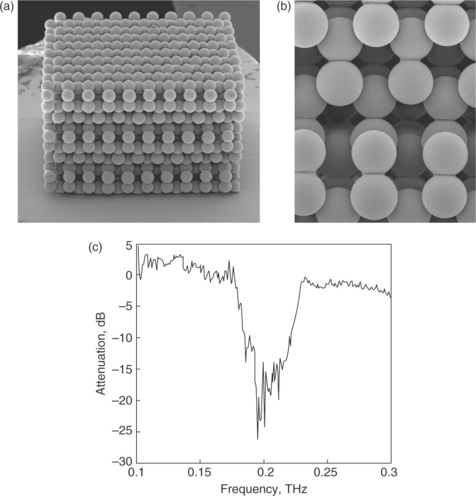
8.10 (a) A picture of a fabricated 3D diamond structure using a laser microwelding method; (b) a close look of the front view of the picture shown in (a); (c) a transmission spectrum of the diamond structure in the <111> crystalline direction (Takagi et al., 2010). Reprinted with permission from IOP Publishing.
8.6 Conclusions
Laser-based methods are expected to find many applications in assembly of photonic, micromechanical, microelectronic and sensor devices. Laser welding and soldering methods are already widely used in manufacture of photonic devices to produce fibre coupled semiconductor lasers in butterfly packages. A laser-assisted rapid polymer bonding method for assembly and encapsulation of photonic and other microscale devices has been developed. The method allows application of the mature high efficiency, low cost diode laser systems in photonic and microelectronic manufacturing. An associated temperature monitoring method using an embedded microsensor array has been developed for process control. Due to the localized nature of temperature change it is necessary to use embedded sensors to achieve in situ temperature monitoring. Laser assembly of polymer spheres has been demonstrated to produce photonic bandgap materials for terahertz applications. A laser microwelding approach is used to assemble a diamond lattice using polymer spheres. It is expected that laser-based polymer joining approaches will find increasing applications in assembly and packaging of photonic devices and structures.
8.7 References
Bardin, F., Kloss, S., Wang, C.H., Moore, A.J., Jourdain, A., De Wolf, I., Hand, D.P. Laser bonding of glass to silicon using polymer for microsystems packaging. IEEE/ASME Journal of Microelectromechanical Systems. 2007; 6:571–580.
Brown, D.M., Dickey, F.M., Weichman, L.S. Multi-aperture beam integration systems. In: Dickey F.M., Holswade S.C., eds. Laser beam shaping: Theory and techniques. New York: Marcel Dekker; 2000:273–311.
Demir, H.V., Zheng, J.F., Sabnis, V.A., Fidaner, O., Hanberg, J., Harris, J.S., Miller, D.A.B. Self-aligning planarization and passivation for integration applications in III-V semiconductor devices. IEEE Transactions on Semiconductor Manufacturing. 2005; 18:182–189.
Dow Chemical. Processing procedures for CYCLOTENE 4000 series photo BCB resins, 2009. http://www.microchem.com/PDFs_Dow/cyclotene_4000_immersion_dev.pdf [Available from:, Accessed 21 December 2011].
Dow Chemical. Cyclotene advanced electronics resins, 2011. http://www.dow.com/cyclotene/solution/index.htm [Available from:, Accessed 21 December 2011].
Jang, S. Packaging of photonic devices using laser welding. SPIE. 1996; 2610:138–149.
Jang, S., Automation manufacturing systems technology for opto-electronic device packaging. Electronic Components and Technology Conference, Las Vegas, 21–24 May 2000, 2000:10–14.
Liu, Y., Zeng, J., Wang, C.H. Accurate temperature monitoring in laser-assisted polymer bonding for MEMS packaging using an embedded microsensor array. IEEE/ASME Journal of Microelectromechanical Systems. 2010; 19:903–910.
Song, J.H., O’Brien, P., Peters, F.H. Optimal laser welding assembly sequences for butterfly laser module packages. Optics Express. 2009; 17:16406–16414.
Streetman, B., Banerjee, S.Solid sate electronic devices. New Jersey: Prentice Hall, 2000.
Takagi, T., Masanori, O., Kawasaki, A. A microsphere assembly method with laser microwelding for fabrication of three-dimensional periodic structures. Journal of Micromechanics and Microengineering. 2010; 20:035032.
Tan, C.W., Chan, Y.C., Leung, B.N.W., Tsun, J., So, A.C.K. Characterization of Kovar-to-Kovar laser welded joints and its mechanical strength. Optics and Lasers in Engineering. 2005; 43:151–162.
Wiedmann, J., Rai, M.M., Ebihara, K., Matsui, K., Tamura, S., Arai, S. Deeply etched semiconductor/benzocyclobutene distributed Bragg reflector laser combined with multiple cavities for 1.5 μm wavelength single-mode operation. Japanese Journal of Applied Physics. 2001; 40:4031–4037.
Wang, C.H., Zeng, J., Liu, Y., Recent advances in laser assisted polymer intermediate layer bonding for MEMS packaging. Proceedings of 10th International Conference on Electronics Packaging Technology and High Density Packaging (ICEPT-HDP), Beijing, 2009:31–35. [10–13 August].
Wong, C.P. Polymers for electronic packaging. In: Harper C.A., ed. Electronic packaging and interconnection handbook. New York: McGraw-Hill; 2000:11–121.
Yagi, H., Onishi, Y., Koyama, K., Ichikawa, H., Yoshinaga, H., Kaida, N., Nomaguchi, T., Hiratsuka, K., Uesaka, K. 1.3 μm wavelength AlGaInAs/InP ridge-wave-guide lasers utilizing benzocyclobutene planarization process. SEI Technical Review. 2009; 69:92–95.