
Fabrication of periodic photonic microstructures by the interference of ultrashort pulse laser beams
Abstract:
The fabrication of periodic photonic microstructures by the interference of ultrashort pulse laser beams has found applications in several fields. This interference can produce a periodically modulated light intensity distribution with a period of the same order as the laser wavelength. A periodically modulated microstructure can be obtained if the periodically modulated light intensity distribution is transferred to a photoreactive material. The interference of two beams creates a onedimensional periodic pattern. In principle, by increasing the number of beams, 2D and 3D periodic patterns can be obtained. This technique (with its unique advantages of being maskless and photoresist-free, with inner encoding for transparent materials and single step processing) has opened up the possibility of fabrication of periodic functional microstructures in a large variety of materials. This chapter discusses the fabrication of periodic photonic microstructures by multi-beam interfered femtosecond laser pulses, and also looks at their applications for photonic devices.
4.1 Review of periodic photonic devices induced by the interference of ultrashort pulse laser beams
Since the first demonstration of the mode-locking technique in 1964, ultrashort pulse lasers have made tremendous progress. In 1964, the laser pulse-width available was down to 100 picoseconds1−3 whilst, by 1981, pulse-widths had been reduced to 100 femtoseconds using the colliding-pulse mode-locking technique.4,5 With successive improvements in passive mode-locking and dispersion compensation, few-cycle pulses (of sub-6 fs) have been obtained.6−8 Recently, laser intensities of 1022 W/cm2 have been achieved.9
Parallel to these breathtaking achievements in ultrashort pulsed lasers, the applications of these lasers have flourished in numerous fields, as a result of their ultrashort and ultra-intense features. Of these, work with interference from ultrashort pulse laser beam-induced periodic photonic devices has made great progress and found applications in various fields.10−25
Femtosecond pulses are characterized by an ultrashort time domain with good coherence over the whole pulse duration. When two or more beams of femtosecond pulses split from one source beam and overlap in both space and time, a periodically modulated light intensity distribution with a period in the order of its wavelength can be produced. Furthermore, a periodically modulated microstructure can be obtained if the periodically modulated light intensity distribution is transferred to a photoreactive material.
Interference, diffraction and polarization are, of course, the three main research topics in wave optics. Since the first demonstration of double-slit interference by Thomas Young, optical interference has been extensively used in a wide range of scientific and technological areas. In recent years, laser interference lithography has also received great attention as it can produce periodic patterns at a micro/nano scale without using a mask.26−29 For conventional interference lithography, interfered continuous wave (CW) or nanosecond laser beams are employed to irradiate a photoresist. After laser exposure, developing, fixing and etching procedures are needed to form the desired periodic microstructures. By comparison, the femtosecond laser interference technique can directly induce periodic microstructures without a photoresist. In addition, with the nonlinear interaction of a femtosecond laser with transparent materials, a periodic microstructure can be fabricated in the interior of these materials.
Section 4.2, below, presents the theoretical aspects of the interference of ultrashort pulse laser beams, including how to make femtosecond pulses overlap. The formation of microstructures by the interference of two femtosecond laser beams and their applications are reported in Section 4.3, whilst Section 4.4 looks at the formation of microstructures by the interference of multi-femtosecond laser beams and their applications. In Section 4.5, the transfer of periodic microstructures by the interference of multi-femtosecond laser beams is reported (combining the femtosecond laser interference technique and the laser-induced forward transfer technique, the transfer of periodic microstructures from a metal film on a supporting substrate to a receiving substrate has been successfully achieved). Finally, Section 4.6 presents a summary and outlook.
4.2 Theoretical aspects of the interference of ultrashort pulse laser beams
4.2.1 How to make femtosecond pulse interference
It is well known that the shorter the pulses, the smaller the area over which the pulses overlap at relatively large angles and with little coherence. For two beams crossed at an angle θ, the size of the overlap area is given by L = cτ(sinθ/2)−1, where c is the speed of light in the medium and τ is the pulse duration.30 For example, for a 120 femtosecond duration and a 30° crossed angle, the beams overlap only within a strip approximately 140 μm wide. The number of interference fringes produced by two beams is independent of the angle and, for transform-limited pulses, is roughly 2cτ/λ, where λ is the optical wavelength.30 With 120-femtosecond pulses at 800 nm, only approximately 90 interference fringes can be produced.
Currently, there are two beam delivery approaches to achieve interference of femtosecond pulses. The first approach is to split the source beam by a mirror beam splitter (MBS), with an optical delay in order to achieve the spatial and temporal interference of femtosecond laser pulses. The second is to split the source beam by a diffractive beam splitter (DBS), which can divide one laser beam into several beams with equal intensity (illustrated in Fig. 4.1), and then to use a confocal imaging system in which no optical delay is needed. For the first approach, precise adjustments of the optical delay for each optical path are needed by observing the sum-frequency generation, or third-harmonic generations,11 to obtain the temporal overlap of the femtosecond pulses; additionally, when the interference of more than two beams is needed, a complicated optical set up is required, the precise adjustment of which is very difficult. For the second approach, the optical set up is quite simple and temporal overlap can be achieved without any adjustment.30

4.1 Beam delivery approaches for femtosecond pulses interference. (a) MBS beam delivery; (b) DBS beam delivery.
The intrinsic difference between the two beam delivery approaches is that, in the case of diffraction off a grating (in the case of MBS), short pulses become tilted, whilst pulses that correspond to different diffraction orders (in the case of DBS) have parallel pulse fronts. Figure 4.2 illustrates this difference.10,30 When the source beam is split by an MBS (Fig. 4.2a), the width of the overlapping area is cτ/sin(θ/2) because the pulse fronts of the two beams are not parallel. When the source beam is split by a DBS (Fig. 4.2b), the width of the overlapping area can reach the beam diameter of the incidence light because the wave fronts of the two beams are parallel. Thus, if a larger overlapping area is required, the second beam delivery approach is a better choice. The disadvantage of the second beam delivery approach, however, is that the power density in the interference plane is lower compared to the first beam delivery approach because the interference area in the second approach is larger than that of the first. It is hard to induce periodic structures on high damage threshold materials for the second approach.

4.2 (a) Overlap of crossed femtosecond beams split by a mirror beamsplitter. (b) Overlap of crossed femtosecond beams split by a transmission grating with a confocal imaging system. (Reproduced from Ref. 10.)
For classification purposes, microstructures induced by using an MBS beam delivery are referred to as microstructures induced by two-beam femtosecond laser interference. Similarly, microstructures induced by using a DBS beam delivery are referred to as microstructures induced by multibeam femtosecond laser interference.
4.2.2 Distribution of optical intensity in the interfered region
To investigate the interference patterns formed by multiple non-coplanar laser beams, we have taken a four-beam interference setup as an example, to deduce the optical intensity distribution within the region of interference.
Extending the different beam interferences is straightforward. Based on electromagnetic wave theory, the plane wave can be expressed as E = Aexp[−i(ωt−k•r)], which can be analyzed in coordinate as:
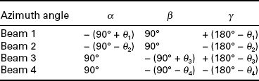
where A, k and ω are amplitude, wave vector and angular frequency of the plane wave, respectively, and α, β and γ are the azimuth angles of the plane wave. In Fig. 4.3 (inset), four laser beams, located in two orthogonal planes, irradiate a sample with incident angles of θ1, θ2, θ3 and θ4, respectively. The azimuth angles of the four beams can be calculated for this figure; see Table 4.1.

4.3 Optical setup for fabrication of periodic microstructures by interfering femtosecond laser beams. DBS: diffractive beam splitter, L1 and L2: lenses, and AA: aperture array. The inset shows the geometry of four-beam interference.
Substituting the azimuth angles of the four beams taken from Table 4.1 into Eq. [4.1], the complex amplitude of the four laser beams can be deduced as:

The complex amplitude of the sum oscillation for the four beams in the interfering field is then:

If we assume that the four beams have equal light intensity and approach the sample with the same angle of incidence (i.e., A1 =A2 = A3 = A4=A and θ1 = θ2 = θ3 = θ4 = θ), then, by combining Eqs. [4.2] and [4.3], we obtain:

and

where, ‘*’ represents the complex conjugate.
Finally, we can get the distribution of light intensity within the interfering field:

Using the relation cos α = (eiα + e −iα)/2, Eq. [4.6] can be simplified to:

Using a similar procedure, the distribution of light intensity for two- and five-beam interference can also be deduced as:
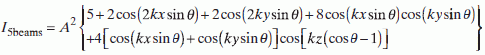
From Eqs. [4.7], [4.8] and [4.9], we can see that for two- and four-beam interference, the intensity distribution is independent of z, while for five-beam interference, it is not. Thus, the structures are basically independent of depth, that is, the same structure is observed in any xy plane in the case of the interference of four beams or less. However, with five-beam interference, the central beam has a different wave vector in the z axis. As a result, the structures obtained by five-beam interference is periodic in the z axis as well as in the x and y axes.
The interference fringe interval can be derived from the distribution of light intensity. For example, for two-beam interference, the period of the fringes, Λ, is given by:
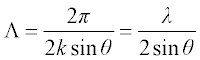
When θ equals 90°, the interference fringes have a minimum period, which is half the wavelength.
4.3 Microstructures induced by the interference of two femtosecond laser beams
4.3.1 Experimental setup
For their experimental setup (schematically shown in Fig. 4.1a), most studies have used a regeneratively amplified Ti:sapphire laser with a wavelength of 800 nm, a pulse duration of 30–200 fs, and a pulse repetition of 1–1000 Hz. A single laser beam is split into two beams that are then redirected at approximately equal incident angles onto a sample surface, focused by two lenses. After the optical paths are adjusted to realize perfect overlap of the two beams both spatially and temporally, the sample surface is adjusted to be approximately normal to the perpendicular bisector of the two incident beams, so that the sample surface becomes the laser interfering plane. A single shot of the femtosecond laser with controlled energy for each interfered beam completes the encoding process.
4.3.2 Formation of periodic microstructures
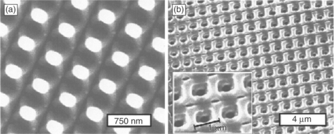
Fabrication of surface relief gratings is the most common application for the femtosecond laser interference technique. The fabrication of surface relief gratings on a variety of transparent dielectrics including silica glass, sapphire, etc. have been extensively investigated by the Hosono group.11−14, 19, 20 Figure 4.4 shows surface relief gratings encoded on amorphous SiO2 bulk glass by irradiation with crossed femtosecond-laser pulses with different incident angles (θ, 10°, 45° and 80°, respectively). The period of grating, d, varies with θ, that is, it is 2.5 μm for 10°, 0.58 μm for 45° and 0.43 μm for 80°. These correspondences confirm the relation for two-beam interference at the surface, according to Eq. [4.10]. In addition, by double exposure,13 dual-structured gratings can be achieved (as shown in Fig. 4.5).

4.4 Surface relief gratings encoded on SiO2 glasses by holographic irradiation of femtosecond-laser pulses. The colliding angle between the two pulses is θ. (Reproduced from Ref. 11.)
4.5 Influence of the beam cross-angle on the shape of resulting double gratings. (a) Two-dimensional array of dual-structured hole is seen for θ = 45°. (b) Double grating encoded under the crossing angle of 90° for both exposures. (Reproduced from Ref. 13.)
Our group (at the Shanghai Institute of Optics and Fine Mechanics) has fabricated surface relief gratings containing noble metal nanoparticles using two-beam femtosecond laser interference.15 Au2O-doped glass samples were first irradiated by two 800 nm interfered femtosecond laser pulses at room temperature and then heat-treated at 550°C to allow Au nanoparticle precipitation in the laser irradiation areas. One-dimensional periodic arrays of the Au nanoparticles were controlled by changing the pulse energy and the incident angle between the interfered laser pulses.
Kaneko et al. demonstrated fabrication of a submicron grating in a metal ion-doped polymer by two-beam femtosecond laser interference with two-photon photoreduction.16
As well as being used for the fabrication of surface relief gratings, two-beam femtosecond laser interference can also induce volume gratings inside transparent materials. Si et al. have fabricated volume gratings inside bulk azodye-doped polymers and perylene-orange-doped hybrid inorganic-organic materials.17,18 The diffraction efficiency of the first-order Bragg gratings can be up to 90%. Figure 4.6 shows a volume and surface relief gratings fabricated in azodye-doped PMMA and the diffraction patterns.

4.6 Optical microscopic photos (a–c) of the photoinduced gratings on the top surface (a), in the interior that is 0.4 mm from the top surface (b), and on the bottom surface of the sample (c). The photo on the right (d) is an orthogonal section image of the gratings observed using a confocal laser scanning microscope. (e) Beam patterns of the zero-order diffraction light (right) and the first-order diffraction light (left). The diffraction efficiency was estimated to be 76%. (Reproduced from Ref. 17.)
It is much more difficult to fabricate volume-type gratings on the surface of non-photosensitive materials than it is to fabricate surface relief gratings. Kawamura et al.19 attribute this to two reasons: first, the nonlinear interaction between a strong laser pulse and a material would deteriorate its coherency; second, free carriers cause enhanced optical absorption. It is known that the peak frequency of the absorption band caused by free carriers, or plasma, which are created almost simultaneously by irradiation from a femtosecond laser pulse, is proportional to (carrier concentration)1/2. This implies that the optical absorption coefficient increases in the infrared (IR) region if the laser is powerful enough to generate carriers. The relaxation time of free carriers is nearly equivalent to the laser pulse duration so that, if the laser pulse duration is stretched, the volume gratings are likely to be encoded inside the material. Kawamura et al. used chirped (0.5–5 ps) IR laser pulse interference to induce volume gratings inside SiO2 glass.19 By moving the focal spot of the interfering laser beam, multi-layer gratings can be induced. Recently, Kawamura et al. have also demonstrated fabrication by a distributed-feedback color center laser in single lithium fluoride crystals, encoding gratings inside crystals using chirped femtosecond laser pulses interference.20
Li et al. have also fabricated multi-layer volume gratings inside nonphotosensitive glass by using common femtosecond pulses,21 though their results are not consistent with Kawamura’s analysis (see above) and further investigation is required.
4.4 Microstructures induced by the interference of multiple femtosecond laser beams
Two-beam interference can induce one-dimensional structures and the double exposure of two-beam interference can induce two-dimensional structures. However, by multi-beam interference, two- or three-dimensional structures can be fabricated in one step. Cai et al. have demonstrated that all 14 Bravais lattices can be realized by the interference of four non-coplanar beams31 and this technique will therefore be able to be used for the fabrication of metamaterials with special electromagnetic properties, such as photonic crystals and optical cloaks.32
4.4.1 Experimental setup
The setup for this experiment is shown schematically in Figs 4.1b and 4.3. A regeneratively amplified Ti:sapphire laser with a wavelength of 800 nm, a pulse duration of 30–200 fs and a pulse repetition of 1 kHz is used as the irradiation source. A DBS (the key element of this setup) splits the incident laser beam into several beams. The split beams are made parallel by a lens, L1, and are then selected by an aperture array to obtain an aimed interference pattern. The selected beams are gathered by an objective, L2, and create interference in a focused region, where the sample is placed. The temporal and spatial overlap of the five beams’ pulses is perfectly achieved on the focal plane of L2; no adjustment for the pulses’ temporal overlap is needed. The distance between L1 and L2 is adjusted to make each beam’s plane wave after lens L2. The outer beams (of equal intensity) are placed symmetrically around the central beam, and make an angle with it. Irradiation power and duration can be adjusted to obtain clear periodic structures.
As examples, three types of samples were tested: a commercial silicon wafer (2 mm thickness), a commercial metallic (Ni) foil (20 μm thickness) and a thin metallic (Al) film deposited on a transparent quartz plate (200 nm thickness) were used. All the experiments were carried out at room temperature in ambient atmosphere.
The fabricated structures were observed by an optical microscope and a scanning electron microscope (SEM). The diffraction characteristics of the fabricated structures were also investigated using an He-Ne laser with a wavelength 633 nm, and with a diode-pumped all solid state laser with a wavelength of 532 nm.
4.4.2 Formation of periodic microstructures on silicon wafer
The formation of periodic microstructures on a silicon surface is important for its application in optoelectronic devices. Many types of micrometer-scale surface structures have been fabricated on the surface of silicon when irradiated by pulsed lasers.33−36 Mazur’s group, for example, created a silicon surface covered with a semi-ordered pattern of sharp conical microspikes by irradiating the surface with a femtosecond laser in the presence of halogen-containing gases.35,36
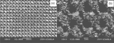
The fabrication of periodic microstructures on silicon wafers has been demonstrated using the interference of five femtosecond laser beams.37 The typical input laser power (incident DBS) was set at 100 mW, whilst the exposure time was ~5 s. Figure 4.7 shows optical and SEM images of the microstructures fabricated by such five-beam femtosecond laser pulses. As can be seen, spots with a diameter of about 300 μm were fabricated in a one-step exposure process (~ 5 s) (Fig. 4.7a). By scanning the silicon wafer, the fabricated spots can be aligned. The detailed structures in the spot are shown in Fig. 4.7b, c and d. A four-fold symmetrical structure was induced on the silicon surface. The period of the array structures was about 2.5 μm. As the exposure time was up to 5 s with a laser power of 300 mW and a 1 kHz repetition rate, the ablated surface deposited much oxidized debris (as shown in Fig. 4.7 d).

4.7 Optical and SEM images of the microstructures on silicon wafer fabricated by five-beam femtosecond laser pulses. (a) SEM images of fabricated spots. (b) and (c) Optical and SEM images for the details of the spots in (a). (d) Amplified SEM images for the details of the spots in (a).
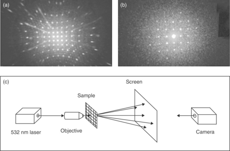
The structures in Fig. 4.7 can be employed as a diffractive beam splitter, as shown in Fig. 4.8. To investigate the diffraction characteristics of the fabricated structures, a diode-pumped all solid state laser with a wavelength of 532 nm was coupled with a 10× optical objective into the structures and the diffraction patterns were recorded by a digital camera; see Fig. 4.8a. With a 532 nm laser wavelength, the induced structure works as a reflective beam splitter. Figure 4.8b shows the diffraction patterns of the periodic structures obtained. Two-order diffraction spots were observed for the periodic structures on a silicon surface. The first-order diffraction efficiency can be defined as the ratio of the averaged power of the first-order diffraction to the power of the zero-order diffraction. The measured diffraction efficiencies of the first-order diffraction spot were 4.84% (for a wavelength of 532 nm) for the periodic structures. The diffraction patterns can be changed by interval and by the shape of the structures, which are related to the laser energy, angle of the beams, focal length and focusing of the lens, irradiation time, laser wavelength, etc.

4.8 Diffraction patterns by the fabricated structures, tested by a 532 nm laser. Diffraction efficiency (averaged first order to zero order) is 4.84%. (a) Experimental scheme for testing the diffraction features. (b) Diffraction pattern.
As already mentioned, there is much debris on the surface of the laser-structured area, which reduces its reflectivity. After washing the surface in an aqueous solution of HF acid to remove the debris, the first-order diffraction efficiency increased to 5.48%.
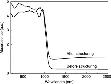
It should be noted that, with a wavelength of 532 nm, there is a high absorption level for silicon within the absorption spectra of the silicon sample (Fig. 4.9). But where there is ‘strong’ absorption, there is also ‘strong’ reflection, and the calculated reflectivity of Si from its optical constants is 37.34% with a wavelength of 532 nm. For IR light with a wavelength of more than 1200 nm, absorption is very low, so that the induced structures can be used as transmission beam splitters for that IR light. In addition, the spectrum ‘after structuring’ shows a higher optical density than that before structuring, because the sample itself acts as a grating, and diffraction losses therefore appear as additional absorption.
4.4.3 Formation of periodic microstructures on metal foil and metal film
For some technological implementations, such as when micrometer-order array holes are necessary, metal materials are required for use in microfabrication. In the case of metal materials with high heat conductivities, the fabrication of micron-order structures by use of ultrashort pulse lasers have unique advantages.38−40 By applying femtosecond laser pulses, the heat-affected zone is in the region of microns in size, allowing the creation of small lateral structures. However, short-pulse irradiation is not necessarily enough to such a small size. The theoretical limit for the smallest spot size achievable is defined by the numerical aperture of the imaging optics and the wavelength of the laser radiation. By decreasing the wavelength, Békési et al. employed a UV femtosecond laser to fabricate micron holes on a metal foil.41 By employing an alternative method, an IR femtosecond laser interference technique, we were able in our experiments to fabricate micrometer-order array holes on both metal foil and metal film.42 With the same experimental setup, we irradiated five-beam interfered femtosecond beams onto Ni-foil and onto Al-film deposited on a glass substrate, using a 150 mW laser (incident DBS), and with an exposure time of ~10 s; the structures fabricated on the Ni-foil are shown in the SEM images in Fig. 4.10. As with the structures fabricated on a silicon wafer, spots with a diameter of about 300 μm were fabricated on the Ni-foil in a one-step exposure process, and four-fold symmetric array holes were induced (with a period of about 2.5 μm). The depth of the ablated holes was about 10 μm (as measured by an optical microscope). As can be seen in Fig. 4.10b, the wall of holes is not very regular, which may be the reason for the longer ablation duration. Based on a two-temperature diffusion model, Chichkov et al. investigated the ablation behaviors of metal during femtosecond laser irradiation37 and proposed that the ablation process could be considered as a direct solid-vapor transition, since very short time scales are involved in the ablation. In our case, the five-beam interference of femtosecond laser pulses produced a periodically modulated light field (the interference pattern) with a distribution of enhanced and weakened intensity. The enhanced optical intensity heated the lattice on a picosecond time scale,38 resulting in the creation of vapor and plasma phases followed by a rapid expansion, and finally forming periodic hole structures on the metal foil.
4.10 SEM photographs of the fabricated array holes on Ni-foil by the interference of five-beam femtosecond laser pulses. (a) SEM image of arrayed holes. (b) Magnified SEM holes in (a).
Figure 4.11 shows the optical and SEM images of array holes fabricated by five-beam interfering femtosecond laser pulses on an Al-film. Similar four-fold symmetric structures were formed on the metal film. The period of the structures was also about 2.5 μm. In the more detailed SEM image in Fig. 4.11b, a particular ‘bead in the hole’ structure can be observed. Beads with a diameter of less than 900 nm are held in each hole. This structure is probably formed by surface tension: during ablation by interfering femtosecond laser pulses, the film is shrunk and torn, forming the ‘bead in the hole’ structure.

4.11 Optical microscope (a) and SEM (b) photographs of the fabricated array holes Al-film by the interference of five-beam femtosecond laser pulses.
The structures in Fig. 4.11 work as diffractive beam splitters, as shown in Fig. 4.12. To investigate the diffraction characteristics of the structures, we coupled a diode-pumped all solid state laser (wavelength 532 nm) with an optical objective lens onto the structures on the metal film, and the diffraction patterns were recorded by a digital camera (see Fig. 4.12a); the experimental setup is presented in Fig. 4.12b. Four-order diffraction spots were observed for the array holes. Here, the diffraction efficiency can be defined as the ratio of the averaged power of every order of diffraction spots to the power of the incident light. The measured diffraction efficiencies of all the order diffraction spots are shown in Fig. 4.12c.

4.12 (a) Diffraction patterns by the structures. (b) Scheme for testing the diffraction. (c) Diffraction efficiency versus diffraction spot order.
Nakata et al. reported the generation of a nano-sized hollow bump array of gold thin film after uniformly spaced melting and inflation of the film induced by a single shot of four interfering femtosecond laser beams,25 and they investigated the transition procedure of the induced periodic structures with increasing laser fluence.
4.5 Transfer of periodic microstructures by the interference of femtosecond laser beams
The laser-induced forward transfer (LIFT) technique has been extensively studied for microprinting of diffractive optical structures and computergenerated holograms,43,44 writing active and passive mesoscopic circuit elements45 and arranging pad arrays in microelectronic packaging,46 etc. The LIFT technique utilizes pulsed lasers to remove a thin film material from a transparent support substrate and deposit it onto a suitable receiving substrate. The LIFT process was first shown by Bohandy et al. to produce direct writing of Cu lines by using single ns excimer laser pulses under a high vacuum.47
By combining the femtosecond laser interference technique and the LIFT technique, transferring of periodic microstructures from a metal Al film deposited on a supporting glass substrate to a receiving glass substrate has been demonstrated.48 Using five-beam interference of near-IR 800 nm femtosecond laser pulses, micrometer-order periodic microstructures were successfully transferred to a receiving substrate, and the characteristics of the transferred structures (as diffractive optics) evaluated and the morphology of the structures investigated using an optical microscope and SEM (see Fig. 4.13).
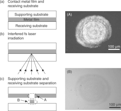
4.13 Schematic of transfer of periodic metal film microstructures by multi-beam interfering femtosecond laser pulses. (a) A receiving substrate is brought onto contact with the metal film deposited on the supporting substrate. (b) Five beams interfering femtosecond laser pulses irradiate the metal film by focusing them on the metal film through the receiving substrate. (c) The supporting substrate and receiving substrate are separated, transferring a periodic microstructure on the receiving substrate, meanwhile leaving a periodic microstructure on the metal film.
The metal film is contacted with a receiving substrate. Two kinds of methods can be applied to focus the interfering laser beams onto the film surface. The first technique (called a front-side transfer), applicable for a transparent receiving substrate, is to focus the interfering beams through the receiving substrate onto the film surface. The second technique (called a rear-side transfer), and used in the case of a transparent supporting substrate, is to focus the interfering beams through the supporting substrate and onto the film surface. In our experiments, both front-side transfer and rear-side transfer could be employed, as the receiving and supporting substrates are both transparent to the laser wavelength. After interfering femtosecond laser irradiation, the supporting substrate and receiving substrate were separated. The induced structure on the supporting substrate and the transferred structure on the receiving substrate were then observed using a 10× optical objective lens, as shown in the inset of Fig. 4.13. As can be seen, the diameters of the induced spot on the supporting substrate and the transferred spot on the receiving substrate are about 300 μm. Concentric circular distributions can be seen in the spots, which were caused by the unequal intensity of the five-beam laser. We measured the intensity of the central beam to be about 20 times greater than that of the other beams. Using a filter can reduce the intensity of the central beam and make the distribution more even.
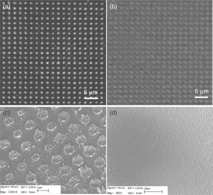
The details of the structures in the spots are shown in Fig. 4.14, which shows optical microscope and SEM images of the microstructures on the supporting substrate (a and c) and on the receiving substrate (b and d). A four-fold symmetric structure was transferred from the supporting substrate to the receiving substrate and a similar structure was also induced on the supporting substrate. The period of structures on both the receiving and supporting substrates was about 2.5 μm. The SEM image of the microstructures on the supporting substrate is clear and debris can be observed around every ablated hole. Although the SEM image of the structures on the receiving substrate illustrates the array structures, the structures look ill-defined when observed at the same amplified ratio as Fig. 4.14c. By adjusting the laser focusing parameters and the thickness of the film on the supporting substrate, the structures on the receiving substrate can be improved as desired.
4.14 Optical microscope and SEM images of the structures on the supporting substrate and on the receiving substrate fabricated by five-beam interference of femtosecond laser pulses. (a) and (c) optical microscope and SEM images of the microstructure on supporting substrate, (b) and (d) optical microscope and SEM images of the microstructure on receiving substrate.
The structures in Fig. 4.14 can work as a diffractive beam splitter (as shown in Fig. 4.15). To investigate the diffraction characteristics of the structures, we again coupled a diode-pumped all solid state laser with wavelength of 532 nm by a 10× optical objective lens into the structures on both the receiving and supporting substrates, the diffraction patterns being recorded by a digital camera (see Fig. 4.15c). Figure 4.15a and 4.15b show the diffraction patterns of the periodic structures on both the receiving and supporting substrates. Four-order diffraction spots and two-order diffraction spots were observed for the periodic structures on the supporting and receiving substrates, respectively. Here, the first-order diffraction efficiency can be defined as the ratio of the averaged power of the first-order diffraction to the power of the incident light. The measured diffraction efficiencies of the first-order diffraction spot for the periodic structures on the supporting and receiving substrates were, respectively, 3.73% and 1.93%. From the diffractive optics of the structures, we can conclude that the structures on the supporting substrate should be periodic holes, whilst the structures on the receiving substrate should be periodic pads. The diffraction patterns can be changed by interval and shape of the holes and pads, which are related to the laser energy, angle of the beams, focal length and focusing of the lens, irradiation time, laser wavelength, etc.
4.15 Diffraction patterns by the microstructures induced on supporting substrate (a) and the microstructures transferred on receiving substrate (b). The averaged diffraction efficiency of first order diffraction spot is 3.73% (a) and 1.93% (b), respectively. (c) Experimental scheme for testing the diffraction by the structures on the supporting substrate and on the receiving substrate.
Adrian et al. investigated the mechanism of metal deposition using the LIFT process.49 They proposed that the LIFT process involves vapor-driven propulsion of metal from a film onto a target. In this case, the periodic holes generated in the supporting substrate are similar to those in a metal foil. The enhanced optical intensity drives the metal vapor onto the receiving substrate to form periodic pad structures, leaving periodic hole structures on the supporting substrate.
The interference transfer technique allows one-step, large-area, micrometer processing of materials for potential industrial applications, such as the fabrication of diffractive optical elements, arranging pad arrays in microelectronic packaging and for the fabrication of sensor elements.
4.6 Conclusions and future trends
This chapter has looked at the fabrication of periodic photonic microstructures by two-beam and multi-beam interfered femtosecond laser pulses. The femtosecond laser interference technique with its unique advantages (being maskless, photoresist-free, with inner encoding and being single step, etc.) has opened up the possibility of fabrication of one-, two- and three-dimensional periodic functional photonic microstructures in a large variety of materials. Additionally, a new technique of transferring periodic microstructures on a metal film from a supporting substrate to a receiving substrate has also been introduced. By adjusting laser energy, beam angles, beam quantity, focal length, irradiation time and laser wavelength, etc., these fabricated structures can be changed in both period and shape.
The possibilities of using femtosecond laser interference for the fabrication of periodic structures with special functions are very promising. For example, fabrication of periodic dots with magnetic properties could be important for current data storage technologies in order to meet demands for increasing storage capacity. Fabrication of periodic dots with fluorescence will find applications in active photonic devices, whilst fabrication of periodic structures with quantum dots inside them will find numerous applications in emerging nano-devices. Fabrication of periodic structures containing DNA could have exciting applications in biomedical fields. Thus, interference fabrication could become a universal tool to prepare designed functional structures. Furthermore, fabrication of special architectures will also find applications in metamaterials and special lattice structured materials.
4.7 Sources of further information and advice
Rullière, Claude Femtosecond laser pulses: Principles and experiments. 2nd, Springer Press; 2003. http://www.google.com/books [available at].
1. Kryukov, P.G. Ultrashort-pulse lasers. Quantum Electronics. 2001; 31:95–119.
2. Bloembergen, N. From nanosecond to femtosecond science. Reviews of Modern Physics. 1999; 71:S283–S287.
3. von der Linde, D., Sokolowski-Tinten, K. The physical mechanisms of short-pulse laser ablation. Applied Surface Science. 2000; 154–155:1–10.
Hosono-Kamiya Laboratory, http://www.khlab.msl.titech.ac.jp
Mazur group, https://mazur-www.harvard.edu
Prof. Kawata’s Cyber Lab, www.skawata.com
4.8 References
1. DiDomenica, M. Small-signal analysis of internal (coupling-type) modulation of lasers. Journal of Applied Physics. 1964; 35:2870–2876.
2. Hargrove, L.E., Fork, R.L., Pollack, M.A. Locking of He-Ne laser modes induced by synchronous intracavity modulation (diffraction by phonons in crystals E). Applied Physics Letters. 1964; 5:4–5.
3. Yariv, A. Internal modulation in multimode laser oscillators. Journal of Applied Physics. 1965; 36:388–391.
4. Fork, R.L., Green, B.I., Shank, C.V. Generation of optical pulses shorter than 0.1 psec by colliding pulse mode locking. Applied Physics Letters. 1981; 38:671–672.
5. Fork, R.L., Shank, C.V., Yen, R., Hirliman, C.A. Femtosecond optical pulses. IEEE Journal of Quantum Electronics. 1983; QE-19:500–506.
6. Morgner, U., Kärtner, F.X., Cho, S.H., Chen, Y., Haus, H.A., Fujimoto, J.G., Ippen, E.P. Sub-two-cycle pulses from a Kerr-lens mode-locked Ti:sapphire laser. Optics Letters. 1999; 24:411–413.
7. Morgner, U., Ell, R., Metzler, G., Schibli, T.R., Kärtner, F.X., Fujimoto, J.G., Haus, H.A., Ippen, E.P. Nonlinear optics with phase-controlled pulses in the sub-two-cycle regime. Physical Review Letters. 2001; 86:5462–5465.
8. Gallman, L., Sutter, D.H., Matuschek, N., Steinmeyer, G., Keller, U., Iaconis, C., Walmsley, I.A. Characterization of sub-6-fs optical pulses with spectral phase interferometry for direct electric-field reconstruction. Optics Letters. 1999; 24:1314–1316.
9. Bahk, S.-W., Rousseau, P., Planchon, T.A., Chvykov, V., Kalintchenko, G., Maksimchuk, A., Mourou, G.A., Yanovsky, V. Generation and characterization of the highest laser intensities (1022 W/cm2). Optics Letters. 2004; 29:2837–2839.
10. Nakata, Y., Okada, T., Maeda, M. Lines of periodic hole structures produced by laser ablation using interfering femtosecond lasers split by a transmission grating. Applied Physics A. 2003; 77:399–401.
11. Kawamura, K., Ito, N., Sarukura, N., Hirano, M., Hosono, H. New adjustment technique for time coincidence of femtosecond laser pulses using third harmonic generation in air and its application to holograph encoding system. Review of Scientific Instruments. 2002; 73:1711–1714.
12. Kawamura, K., Ogawa, T., Sarukura, N., Hirano, M., Hosono, H. Fabrication of surface relief gratings on transparent dielectric materials by two-beam holographic method using infrared femtosecond laser pulses. Applied Physics B. 2000; 71:119–121.
13. Kawamura, K., Sarukura, N., Hirano, M. Periodic nanostructure array in crossed holographic gratings on silica glass by two interfered infrared-femtosecond laser pulses. Applied Physics Letters. 2001; 79:1228–1230.
14. Kawamura, K., Sarukura, N., Hirano, M., Hosono, H. Holographic encoding of fine-pitched micrograting structures in amorphous SiO2 thin films on silicon by a single femtosecond laser pulse. Applied Physics Letters. 2001; 78:1038–1040.
15. Qu, S., Qiu, J., Zhao, C., Jiang, X., Zeng, H., Zhu, C., Hirao, K. Metal nanoparticle precipitation in periodic arrays in Au2O-doped glass by two interfered femtosecond laser pulses. Applied Physics Letters. 2004; 84:2046–2048.
16. Kaneko, K., Sun, H., Duan, X., Kawata, S. Two-photon photoreduction of metallic nanoparticle gratings in a polymer matrix. Applied Physics Letters. 2003; 83:1426–1428.
17. Si, J., Qiu, J., Zhai, J., Shen, Y., Hirao, K. Photoinduced permanent gratings inside bulk azodye-doped polymers by the coherent field of a femtosecond laser. Applied Physics Letters. 2002; 80:359–361.
18. Qian, G., Guo, J., Wang, M., Si, J., Qiu, J., Hirao, K. Holographic volume gratings in bulk perylene-orange-doped hybrid inorganic-organic materials by the coherent field of a femtosecond laser. Applied Physics Letters. 2003; 83:2327–2329.
19. Kawamura, K., Hirano, M., Kamiya, T., Hosono, H. Holographic writing of volume-type microgratings in silica glass by a single chirped laser pulse. Applied Physics Letters. 2002; 81:1137–1139.
20. Kawamura, K., Hirano, M., Kurobori, T., Takamizu, D., Kamiya, T., Hosono, H. Femtosecond-laser-encoded distributed-feedback color center laser in lithium fluoride single crystals. Applied Physics Letters. 2004; 84:311–313.
21. Li, Y., Watanabe, W., Yamada, K., Shinagawa, T., Itoh, K., Nishii, J., Jiang, Y. Holographic fabrication of multiple layers of grating inside soda–lime glass with femtosecond laser pulses. Applied Physics Letters. 2002; 80:1508–1510.
22. Kondo, T., Matsuo, S., Juodkazis, S., Misawa, H. Femtosecond laser interference technique with diffractive beam splitter for fabrication of three-dimensional photonic crystals. Applied Physics Letters. 2001; 79:725–727.
23. Kondo, T., Matsuo, S., Juodkazis, S., Mizeikis, V., Misawa, H. Multiphoton fabrication of periodic structures by multibeam interference of femtosecond pulses. Applied Physics Letters. 2003; 82:2758–2760.
24. Nakata, Y., Okada, T., Maeda, M. Fabrication of dot matrix, comb, and nanowire structures using laser ablation by interfered femtosecond laser beams. Applied Physics Letters. 2002; 81:4239–4241.
25. Nakata, Y., Okada, T., Maeda, M. Nano-sized hollow bump array generated by single femtosecond laser pulse. Japanese Journal of Applied Physics. 2003; 42:L1452–L1454.
26. Zaidi, S.H., Brueck, S.R.J. Multiple-exposure interferometric lithography. Journal of Vacuum Science & Technology B. 1993; 11:658–666.
27. Choi, J.O., Akinwande, A.I., Smith, H.I. 100 nm gate hole openings for low voltage driving field emission display applications. Journal of Vacuum Science & Technology B. 2001; 19:900–903.
28. Pati, G.S., Heilmann, R.K., Konkola, P.T., Joo, C., Chen, C.G., Murphy, E., Schattenburg, M.L. Generalized scanning beam interference lithography system for patterning gratings with variable period progressions. Journal of Vacuum Science & Technology B. 2002; 20:2617–2621.
29. Solak, H.H., David, C. Patterning of circular structure arrays with interference lithography. Journal of Vacuum Science & Technology B. 2003; 21:2883–2887.
30. Maznev, A.A., Crimmins, T.F., Nelson, K.A. How to make femtosecond pulses overlap. Optics Letters. 1998; 23:1378–1380.
31. Cai, L.Z., Yang, X.L., Wang, Y.R. All fourteen Bravais lattices can be formed by interference of four noncoplanar beams. Optics Letters. 2002; 27:900–902.
32. Valentine, J., Li, J., Zentgraf, T., Bartal, G., Zhang, X. An optical cloak made of dielectrics. Nature Materials. 2009; 8:568–571.
33. Fauchet, P.M., Siegman, A.E. Surface ripples on silicon and gallium arsenide under picosecond laser illumination. Applied Physics Letters. 1982; 40:824–826.
34. Lu, Y.F., Choi, W.K., Aoyagi, Y., Kinomura, A., Fujii, K. Controllable laser-induced periodic structures at silicon–dioxide/silicon interface by excimer laser irradiation. Journal of Applied Physics. 1996; 80:7052–7056.
35. Her, T.H., Finlay, R.J., Wu, C., Deliwala, S., Mazur, E. Microstructuring of silicon with femtosecond laser pulses. Applied Physics Letters. 1998; 73:1673–1675.
36. Wu, C., Crouch, C.H., Zhao, L., Carey, J.E., Younkin, R., Levinson, J.A., Mazur, E., Farrell, R.M., Gothoskar, P., Karger, A. Near-unity below-band-gap absorption by microstructured silicon. Applied Physics Letters. 2001; 78:1850–1852.
37. Zhao, Q.Z., Qiu, J.R., Jiang, X.W., Zhao, C.J., Zhu, C.S. Formation of array microstructures on silicon by multibeam interfering femtosecond laser pulses. Applied Surface Science. 2005; 241:416–419.
38. Chichkov, B.N., Momma, C., Nolte, S., von Alvensleben, F., Tuenermann, A. Femtosecond, picosecond and nanosecond laser ablation of solids. Applied Physics A. 1996; 63:109–115.
39. Simon, P., Ihlemann, J. Ablation of submicron structures on metals and semiconductors by femtosecond UV-laser pulses. Applied Surface Science. 1997; 110:25–29.
40. Pronko, P.P., Dutta, S.K., Squier, J., Rudd, J.V., Du, D., Mourou, G. Machining of sub-micron holes using a femtosecond laser at 800 nm. Optics Communications. 1995; 114:106–110.
41. Békési, J., Klein-Wiele, J.-H., Simon, P. Efficient submicron processing of metals with femtosecond UV pulses. Applied Physics A. 2003; 76:355–357.
42. Zhao, Q.Z., Qiu, J.R., Zhao, C.J., Jiang, X.W., Zhu, C.S. Formation of array holes on metal-foil and metal-film by multibeam interfering femtosecond laser beams. Chinese Physics. 2005; 14:1181–1184.
43. Mailis, S., Zergioti, I., Koundourakis, G., Ikiades, A., Patentalaki, A., Papakonstantinou, P., Vainos, N.A., Fotakis, C. Etching and printing of diffractive optical microstructures by a femtosecond excimer laser. Applied Optics. 1999; 38:2301–2308.
44. Zergioti, I., Mailis, S., Vainos, N.A., Papakonstantinou, P., Kalpouzos, C., Grigoropoulos, C.P., Fotakis, C. Microdeposition of metal and oxide structures using ultrashort laser pulses. Applied Physics A. 1998; 66:579–582.
45. Chrisey, D.B., Pique, A., Fitz-Gerald, J., Auyeung, R.C.Y., McGill, R.A., Wu, H.D., Duignan, M. New approach to laser direct writing active and passive mesoscopic circuit elements. Applied Surface Science. 2000; 154–155:593–600.
46. Bähnisch, R., Groß, W., Menschig, A. Single-shot, high repetition rate metallic pattern transfer. Microelectronic Engineering. 2000; 50:541–546.
47. Bohandy, J., Kim, B.F., Adrian, F.J. Metal deposition from a supported metal film using an excimer laser. Journal of Applied Physics. 1986; 60:1538–1539.
48. Zhao, Q.Z., Qiu, J.R., Zhao, C.J., Jiang, X.W., Zhu, C.S. Optical transfer of periodic microstructures by interfering femtosecond laser beams. Optics Express. 2005; 13:3104–3109.
49. Adrian, F.J., Bohandy, J., Kim, B.F., Jette, A.N. A study of the mechanism of metal deposition by the laser-induced forward transfer process. Journal of Vacuum Science & Technology B. 1987; 5:1490–1494.