
Emerging pulsed laser deposition techniques
R.W. Eason, T.C. May-Smith, K. Sloyan, R. Gazia, M. Darby and A. Sposito, University of Southampton, UK
Abstract:
This chapter describes our progress to date in the growth of thin film optical waveguides using both single-beam and multiple-beam/multiple-target geometries using single-crystal garnet targets. More than one target offers the possibility of tuning both the optical and physical properties of the films produced via control of the temporal sequencing of the laser plumes from separate targets. Mixed, layered and superlattice growth, which involve vertical engineering of the film structure, allow precise control of the refractive index profile, a fundamental parameter in the design of optical waveguides. Multi-plume geometries can also be used to structure the thin film in the horizontal plane, for fabricating complex buried structures, a valuable capability for designing thin disk lasing devices.
2.1 Current state-of-the-art in pulsed laser deposition (PLD)
While the use of pulsed lasers for deposition of thin films from laser-produced plasmas dates back more than 40 years, it was not until the late 1980s that pulsed laser deposition (PLD) was demonstrated to be a viable technique for growing functional materials with useful end applications. These early publications addressed the growth of thin films of high temperature, superconducting complex quaternary oxides (Dijkkamp et al., 1987), and it is these first reports of successful growth by PLD that continue to fuel activities within the thin film materials community using this rapid, flexible and comparatively simple method for growing a vast array of single- and multi-component materials (Eason, 2007).
As outlined in the previous chapter, in its simplest form PLD is a physical vapour deposition process that involves four basic components: a pulsed laser (typically a nanosecond pulse duration UV laser such as an excimer), a vacuum chamber, a target that provides the necessary source of atoms and ions for deposition and a suitable substrate located some few centimetres from the target, on which the desired film can grow. Even with this basic level of equipment, thin films can be grown at a rate of a few microns per hour, using a typical 10 Hz pulsed UV laser with ~ 100–500 mJ per pulse, over a substrate area of ~ 1 cm2. If substrate heating is required, which is a routine requirement for growth of single-crystal films, then a radiative or filament-based heater can be used, and temperatures of order 800°C are easily achievable. The choice of substrate will reflect the usual requirements for epitaxial growth, which necessitates appropriate lattice matching between the single-crystal substrate and the crystalline thin film.
In the area of photonic structures, PLD has enormous benefit in both rapid prototyping, and also the ability to grow dielectrics, single crystals, glasses and functional materials such as piezoelectrics, ferroelectrics and transparent conducting oxides. Where there are restrictions such as crosscontamination, which present severe problems in molecular-beam epitaxy (MBE) growth for example, where minute traces of Li can severely alter the desired mobilities for a particular semiconductor device structure, PLD is much more tolerant, and optical hosts such as different compound oxides can be grown sequentially in the same chamber. Current activity in optical waveguide growth, planar optical sensors, microwave devices and surface acoustic wave devices as described in Eason (2007) illustrates the intrinsic versatility of photonic material growth, and this is an increasingly viable technique for research and development activity.
A typical schematic of a PLD chamber is shown in Fig. 2.1, which also shows details of the vacuum pumps and gas handling services. Typically, for growth of oxide materials, a background gas pressure of ~ 10−2 mbar of oxygen is used, although other gases such as nitrogen or argon or even ammonia can also be useful, for both moderating the dynamics and kinetics of the laser plume and also as a source of nitrogen (from laser dissociation of the NH3), if nitride growth is the intended goal, for example.

2.1 Schematic of a single-beam/single-target PLD chamber incorporating indirect laser heating of substrates.
Also shown in Fig. 2.1, however, is a more sophisticated and controllable mechanism for heating of the substrate: a CO2 laser operating at a wavelength of 10.6 μm. The beam can be either focused and raster-scanned across the substrate or spatially re-formatted into a square profile ideally matching the exact size of the substrate (May-Smith et al., 2007a). Laser heating is an extremely efficient method, as almost all substrates that are routinely used for PLD growth absorb strongly at 10.6 μm, and a laser power of ~ 25 W is capable of heating 1 cm2 substrates to temperatures of > 1000°C. Additionally the use of a non-contact heating method means that substrates can easily be rotated while being heated, potentially resulting in much more uniform film growth.
Shown in Fig. 2.2a is a raster-scanned pattern of the incident CO2 laser beam (made visible by the collinear visible red diode laser witness beam) for a stationary substrate. In contrast, a circular ring pattern, like that in Fig. 2.2b, allows the substrate to be rotated while still experiencing a uniform heating profile. Such an arrangement is far from standard on most PLD set-ups, but the flexibility to heat while rotating the substrate is of tremendous value. The substrate is held during rotation by alumina supports, resulting in minimal heat-sinking of the substrate. Using a CO2 laser power of ~ 100 W has allowed us to reach a temperature of greater than 2000°C, sufficient to melt a single-crystal sapphire substrate (melting temperature of 2040°C). Other advantages of non-contact laser heating are the faster substrate temperature ramping and benefits in terms of reduced chamber temperature from such a localised lower total power requirement.

2.2 (a) Substrate under CO2 laser heating via an 8 × 8 point raster scan. (b) Substrate under CO2 laser heating via concentric circle profile patterning.
Numerous laboratories use such PLD facilities to grow thin films for materials research applications, but there are few organisations that undertake commercial research, where wafer-scale films are the accepted standard. For substrates that are larger than a few square centimetres, the necessarily higher laser energy can become prohibitive – single pulse energies of more than 1 J are required. An alternative procedure of automated target tilting during growth may be used, so that the laser plume can be ‘spray-painted’ across the surface of the substrate. However, this also has drawbacks, as the elemental distribution within the plume can be angularly dependent, and hence the stoichiometry of the film may no longer mirror the stoichiometry of the original target, an end result that is not usually desirable.
2.2 Problems for growth of thick films and designer refractive index profiles
An area of particular interest for PLD-grown thin films is the fabrication of optical waveguides, where both the substrate and final thin film are both in single-crystal format. Techniques such as evaporation, sputtering and other physical vapour deposition approaches are in general not suitable for growth of single-crystal optical materials. Amorphous or even polycrystalline films are often unsuitable for optical applications, as are films with unacceptably high propagation losses in-plane. If the material being deposited is isotropic (for example the cubic crystalline garnet hosts as discussed later) then poly-crystallinity is much less problematic, as the propagating light does not see any significant variation in refractive index, which would lead to optical scattering and hence unacceptably high values of optical loss. If, however, the thin film material is anisotropic (for example uniaxial or biaxial crystals) then polycrystallinity or disordered structures can produce extremely lossy films, which render them effectively useless for any final waveguide applications. Aligned epitaxial single-crystal films are therefore the prime end goal of our waveguide growth programme.
2.2.1 Growth of thick optical films
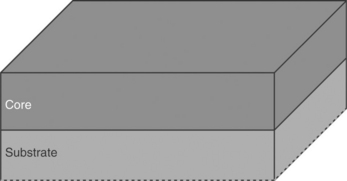
The next and most important aspect of optical waveguides concerns the thicknesses required to allow the propagation of fundamental mode optical beams: in almost all cases we wish to grow waveguides that will only guide the lowest order Gaussian spatial profile. The thicknesses needed in turn depend on the refractive index difference between the core that guides the mode, and the substrate, as illustrated schematically in Fig. 2.3. Optical waveguiding also requires that the core has a higher refractive index than the substrate.
For practical optical waveguides grown from targets doped with an active lasing ion, for example Nd in the crystal host Y3Al5O12 (YAG), the inclusion of a typical dopant concentration of ~ 1% will only raise the refractive index by around 0.1%. If the substrate is also YAG, for example, relatively thick waveguides of ~ 10 μm are hence required for fundamental mode propagation. Such homoepitaxial growth is comparatively straightforward, but waveguide thicknesses of 10 μm may take a comparatively long time to grow. Heteroepitaxial growth of another garnet with much higher refractive index than the substrate, for example Gd3Ga5O12 (GGG), whose refractive index is higher than YAG by around 7%, may be preferable, as single mode guiding can be achieved in a much thinner film.
Table 2.1 comprises a list of garnet crystals that we have investigated so far, which includes the previously mentioned YAG and GGG. Immediately apparent are the differences in both thermal expansion coefficient and lattice constant for this range of garnets, so that there is an intrinsic mismatch between the substrate and core. Lattice mismatch is rarely a significant problem for thick film growth as the lattice of the film will fully relax to its natural value some small distance (of order ~ 1 μm) from the interface, and the presence of the interfacial defects does not usually pose much of a problem. A lattice mismatch of a few per cent is readily accommodated in single-crystal PLD growth. For thicknesses of a few microns, mismatches of < 5% are acceptable (Tomashpolskii and Sevostianov, 1980) while for PLD growth where bonding is weak, and epitaxy occurs via island growth, a lattice mismatch of > 13% has been reported (Wang et al., 1991). More serious, however, is the mismatch in thermal expansion coefficients; a film grown at 800°C, for example, can exhibit severe distortion when cooled down to room temperature and removed from the chamber, to the extent that the substrate is bent from its original flatness into a shape as shown (with some exaggeration) in Fig. 2.4. Providing the deformation is within reasonable limits, most structures will survive this degree of bending, and do not show signs of cracking or delamination. However, the end-face polishing step that is a prerequisite for efficient launching of light into the waveguide will often cause the inbuilt tensile or compressive stress to be released. The core can shatter as a result, even to the extent of cracking the substrate into several pieces.
Table 2.1
Physical properties of nine garnet crystals

Note: Where ‘—’ appears, no reliable data have yet been found in the literature.
Source: After May-Smith and Eason (2007).
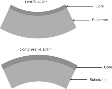
2.4 Schematic of effects of cooling from elevated temperature on thick PLD films with dissimilar thermal expansion coefficients between core and substrate.
Film thicknesses of up to ~ 1 μm are generally not subject to such problems; however, it is experimentally difficult to efficiently launch light into so thin a waveguide. We have grown films of Nd-doped GGG on YAG at thicknesses of >100 μm, all of which have undergone cracking, particularly where two end faces meet and the tension/compression is a local maximum. Growth of films of several tens of microns thickness required for multi-mode planar amplifier structures also often result in cracking or poor yield. What is needed is a growth methodology that yields films that are tolerant to thermal coefficient mismatch (May-Smith et al., 2011) and/or uses combinations of several targets to grow films whose properties, such as expansion coefficient, can be averaged to more closely match that of the substrate. We will return to this topic in subsequent sections where we discuss multiple target PLD geometries.
2.2.2 Choice of targets and minimisation of particulates
Since the very first demonstration of the PLD technique, one of its chief limitations has been the presence of ‘particulates’ in the film being deposited. These particulates are small (nanometre to micron-scale particles), and can originate both from the laser–target interaction, via the liquid phase and subsequent ‘splashing’ and exfoliation, and during the plasma transport to the substrate. Such particulates are a permanent distraction and their removal is a universal goal for all engaged in PLD research. Of particular annoyance for optical waveguide applications is the fact that particulate size is comparable to the optical wavelengths used, and hence scattering and waveguide propagation loss is a constant problem.
Particulate removal has been attempted by many groups using a wide variety of techniques, including velocity filtering (Yoshitake and Nagayama, 2004), shutters (Chen, 1994), synchronised pulsed gas jets (Barrington et al., 2000) and also use of ultra-short pulse (picosecond and femtosecond) lasers (Gamaly et al., 2007). It is now accepted, however, that all single-target geometries will suffer from particulate problems to a greater or lesser extent. One simple solution that at least mitigates the problems of particulates lies in the nature of the target itself. For high quality optical waveguide growth, we routinely use single-crystal (and hence fully dense) targets. If alternative sintered or compressed target materials are used, then the inevitable reduction of density from the ideal 100% of ‘bulk’ value leads to the presence of voids, or other inclusions, and these are a ready source of particulate generation.
Composite or sectored multi-component targets can also be used in single-beam PLD, in an attempt to grow films whose composition reflects the target geometry. In its most simple implementation, a sector target as shown in Fig. 2.5a can be fabricated, but this is usually made from sintered precursors so again suffers from the problems of particulates. An obvious alternative, and one that uses single-crystal targets, is shown in Fig. 2.5b; by controlling the point of incidence of the pulsed laser, as well as the rotation speed and/or pitch of the lead-screw, multi-component laser plumes can be generated.
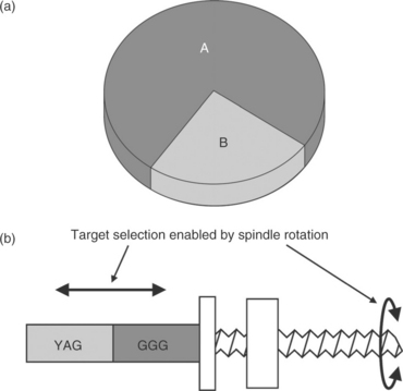
2.5 (a) Composite sector target of dissimilar materials A and B. (b) Composite target formed by joining of two dissimilar rods.
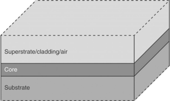
In practice, a more favourable approach can be to move to multi-target and multi-beam geometries, discussed in detail in Section 2.3. However, before we leave single-beam geometries behind us, one final point needs to be made concerning particulates: if you can’t eliminate them, then one option is to deposit more material over them. In the case of cubic and hence optically isotropic garnet films, particles present within the volume of the film, that have since been buried, will contribute little to the final loss of the optical waveguide grown, provided the surface density of particles is not excessive. Admittedly, for a simple core/substrate waveguide, the optical mode does sample the top surface layer of the core region, and hence particulates are a problem on the surface. In this case, the solution is to grow a capping or superstrate layer, as shown in Fig. 2.6, so that the final wave-guiding region itself is buried. Surface contamination of the top surface of the superstrate is then no longer a contributing factor to final waveguide propagation loss. To date, and as a benchmark of the quality of the garnet films grown by PLD so far, the lowest loss reported in a doped GGG on YAG waveguide was less than 0.1 dB cm−1 (Grivas et al., 2004; May-Smith et al., 2004).
2.3 Multi-beam PLD
With only a very few exceptions, such as the work reported in György et al. (2006) and Kompitsas et al. (2007), the use of more than one laser source to perform PLD is so far uncommon. If sequential deposition of materials is required to fabricate layered or mixed compounds, then target carousels can be used and specific targets selected as appropriate. However, if more sophisticated multilayers (addressed in a later section) are required and many thousands of sequential depositions are needed, then it becomes increasingly impractical to alternate targets at timescales of potentially once per second. However, growth from two (or more) different targets using a single laser source can yield high-quality structures (see Fig. 2.7).
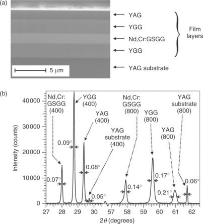
2.7 (a) SEM image of five layer symmetric multilayer structure (after May-Smith et al., 2007b). (b) XRD spectrum of multilayer structure shown in (a). (after May-Smith et al., 2007b)
Figure 2.7a shows moderately thick (1–2 μm) single-crystal layered growth of YGG (Y3Ga5O12), and the Nd and Cr doped quaternary garnet GSGG (Nd,Cr:Gd3Sc2Ga3O12), with YAG as both substrate and superstrate (May-Smith et al., 2007b). The excellent crystallographic quality is shown in Fig. 2.7b, where all XRD peaks are clearly depicted for each single-crystal layer. Note, however, that due to non-optimised growth conditions for the YAG capping layer, the PLD-grown YAG shows an XRD peak position that is not coincident with the YAG substrate. This situation is not uncommon in all our PLD-grown garnets, as the basic garnet formula of A3B5O12 is tolerant to variation between the A and B atomic ratios. This topic will be re-addressed in Section 2.3 when we consider Ga content in GGG growth via multi-beam deposition for stoichiometric correction.
2.3.1 Multi-target, multi-beam geometry
Shown in Fig. 2.8a is the multi-target PLD set-up, which has three separately controllable lasers that can be directed to three separate targets, T1,2,3. This arrangement now brings an enormous further potential to PLD growth, as the three laser plumes generated can be synchronous, time-delayed or of different relative strengths or repetition rates, and films can be grown that have graded, layered, superlattice, or fully mixed character. Shown in Fig. 2.8b is a close-up picture of the three target assembly with three different single-crystal garnet targets in place. Each target rotates and has a programmable tilt capability for directional plume management. The rest of this chapter will therefore address a range of these possibilities, and show our progress to date in implementing such novel film geometries.

2.8 (a) Schematic of three laser/three target PLD set-up with independently addressable targets and laser-heated rotatable substrate (after Eason et al., 2009). (b) Close-up view of three target assembly. Each target rotates and also has adjustable tilt angle.
2.3.2 Layered growth: different targets with plumes temporally coincident
This arrangement is the next logical extension to the results presented in Section 2.3, but involves growth from more than one target, and mixed layers can therefore be produced. For optical waveguide growth this is exactly what is needed for producing specific refractive index profiles for the core region, or the interfacial layers that form the core–cladding boundaries. This mixed layer approach also presents the intriguing possibility of engineering not only refractive index but also thermal expansion coefficient, where the properties of each separate target T1,2,3 can be averaged in the ratio of their intrinsic values and their relative abundances in the final film. As an example, we consider the three garnets GSGG, GGG and Y3S2Ga3O12 (YSGG), where a mixed film of GSGG and GGG is grown on a YSGG substrate. The aim is to grow a waveguiding layer with the requisite refractive index higher than that of the substrate, but with the thermal expansion coefficient matched as closely as possible, to eliminate the bending and/or cracking on cooling to room temperature discussed earlier. Using the data as in Table 2.2, it is easy to design the correct a priori recipe for growth, under the assumption that such mixing and averaging of materials properties holds true.

Figure 2.9 illustrates such a scenario whereby materials mixing can produce a waveguide structure whose end properties are closely matched using a film grown with a composition ratio of 66% GSGG to 33% GGG. Of particular relevance is the fact that matching of thermal expansion coefficient and lattice constant (to a difference of less than 0.4%) should be possible between film and substrate, while maintaining the required higher refractive index for the core. With this design concept in mind, a test structure was grown incorporating such hybrid garnet phases, using GGG and YSGG as the film constituents; YSGG was chosen over GSGG for this test as a target was already available. The structure consisted of seven layers arranged symmetrically to achieve a symmetrical refractive index profile. The compositions and sequence of the layers are shown in Table 2.3. Layers 1 and 7 are made of pure YSGG, layers 2 and 6 are made of Nd:GGG and YSGG mixed in the ratio 1:2, layers 3 and 5 consist of the same precursors but mixed in a ratio 2:1, and finally layer 4 is the core of the waveguide and is made from Nd:GGG (Gazia et al., 2008).
Table 2.3
Deposition parameters for each of the seven layers in the multilayer sample

Source: After Gazia et al. (2008).

2.9 Schematic of planar waveguide structure of GSGG + GGG grown on a YSGG substrate, and estimate of materials properties derived though simple averaging.
The growth time here is long, as the lasers used for ablation were low energy (100 mJ per pulse) Q-switched frequency quadrupled Nd:YAGs, whose wavelength of 266 nm is longer than the more conventional excimer wavelengths of 248 or 193 nm. However, the aim here was to determine whether such mixed layers could be grown, and to look at their crystal quality and final stoichiometry. Shown in Fig. 2.10a is a schematic of the layered film structure, while in Fig. 2.10b is an energy dispersive X-ray analysis (EDX) line scan of elemental composition acquired from a cross-sectional region of the film. It is clear (within the limited spatial resolution afforded by EDX) that the elemental composition follows the intended growth profile and that the final ~ 10 μm thick structure is indeed fully single crystal, as identified by XRD (not shown here) where peaks corresponding to each separate garnet phase as well as the hybrid mixed phases are seen. As a final example of the growth of an even more complicated layered structure, Fig. 2.11 shows the results for a thinner 11 layer composite, again using GGG and YSGG garnet targets (Eason et al., 2009).

2.10 (a) Schematic of seven layer symmetric waveguide grown on a YAG substrate (after Gazia et al., 2008). (b) EDX line scan results of elemental composition overlaid on a schematic of the structure in (a). (after Gazia et al., 2008)

2.11 Composite picture of design schematic, SEM image and EDX line scan of scandium concentration in an eleven layer symmetric structure (after Eason et al., 2009).
2.3.3 Mixed growth: different targets with plumes temporally coincident
As well as growing layers that are intended for optical waveguide end applications, there is an even more obvious need to grow materials as single layer films, where the stoichiometry can be tuned by growth from more than one target. As has been mentioned in Section 2.3, Ga is an element whose concentration in the final film can be less than that present in the target due to preferential re-sputtering from the growing film, as well as its intrinsic volatility and low melting point. Both can routinely lead to a deficiency of ~ 10% compared to the ideal 5:3 ratio between Ga and Gd in stoichiometric GGG, for example. If two targets are used, one being a standard GGG single-crystal target while the other is gallia (Ga2O3), then by varying either the number of pulses used for each target, or the laser fluence used to ablate either target, an empirical correction procedure can be adopted to alter the final Ga concentration in the resultant film.
As a demonstration of this dual beam (T1 = GGG, T2 = Ga2O3) technique, a series of eight depositions were performed under different relative values of fluence for T1 and T2 while all other parameters were kept the same. Figure 2.12 shows a composite XRD plot for five of the films that showed XRD peaks together with the values of Gd/Ga ratio as determined by EDX analysis (Darby et al., 2008). It is seen that compositions that are both Ga deficient, (Gd/Ga > 0.6) and, more surprisingly, Ga rich (Gd/Ga < 0.6) can be grown; this situation is far from our normal experience when growing from single stoichiometric targets, which are almost always Ga deficient by ~ 10%. The introduction of an increasing amount of gallium from the Ga2O3 target is shown to decrease the lattice parameter of the GGG film (XRD peak appears at higher values of 2θ) and, for an optimum fluence used on the Ga2O3 target, make the film closer to stoichiometric GGG. The lattice shifting from the database stoichiometric value is believed to occur due to a varying amount of Gd3+ occupying lattice sites that would usually be occupied by Ga3+, but are left open due to a Ga deficiency in the films. For Ga concentrations above that of stoichiometric GGG, the lattice parameter continued to reduce. This is thought to be due to the occupation of some lattice sites normally occupied by Gd3+ by the excess Ga3+ and/or to the incorporation of the excess Ga in the lattice in the form of defects.

2.12 Composite XRD spectra of five films deposited with various fluences on the Ga2O3 and Nd:GGG targets of (a) 1.7 and 1.5 J/cm2, (b) 1.7 and 2.3 J/cm2, (c) 1.1 and 2.3 J/cm2 and on the Nd:GGG target only of (d) 2.3 J/cm2, (e) 1.5 J/cm2. The dotted line corresponds to the position of the (400) GGG peak for stoichiometric composition (2θ = 28.839°). The intensities of the GGG (400) peaks have been normalised (after Darby et al., 2008).
This mixed growth PLD approach brings increased flexibility and control, specifically for materials that have previously proven difficult to deposit with their ideal stoichiometric composition. A critically important application of this technique is the minimisation of the lattice mismatch between the film and the substrate by choosing a combination of materials, when mixed in the correct ratio, that will grow with the appropriate lattice parameter. An additional bonus to using multiple targets lies in adopting the ‘cross-beam’ geometry that has been successfully adopted in Gaponov et al. (1982) and Gorbunoff (2007) to minimise the concentration of particulates present in the final film.
As seen in Fig. 2.13, a suitable blockage placed in front of the substrate can provide a geometrical line-of-sight barrier to the incidence of particulates. These particulates, being massive in comparison to the atoms and ions present in the plasma plumes, are ballistic in nature and travel in essentially straight lines, thereby reaching the growing film in much fewer numbers that would be present with a single-target geometry. The atomic and ionic constituents of the laser plasma, however, will undergo numerous collisions during their transit to the substrate, and hence experience a deflection along the direction of their common intersection. An ideally particulate-free film should result, albeit with a relatively low growth rate. The expansion to three plasma sources (not yet attempted by us) allows out-of-plane plasma plume interactions and this has implications for even better particulate trajectory and removal strategies.

2.13 Schematic of cross-beam PLD technique for minimising particulates on the substrate (after Gorbunoff, 2007).
2.3.4 Layered growth: different targets and plumes temporally alternating
A further implementation involves two different targets and depositions that are no longer temporally coincident, with the intention of producing layered growth of materials whose thicknesses are controlled by the relative number of pulses on each target. For materials that have a compatible set of growth parameters, this is easy to achieve, and, as shown in Fig. 2.14, a simple mechanical shutter arrangement can be used, under computer-programmable control.

2.14 Schematic of dual-target PLD chamber with programmable shutter control (after Sloyan et al., 2010).
Targets T1 or T2 can be ablated simultaneously, to grow a mixed film as in Section 2.3.3, or sequentially, to grow multilayered structures. As a preliminary experiment, ten samples were grown and characterised via XRD in order to determine the number of pulses required to produce a film where individual layers of materials from these dissimilar targets can be resolved. The number of pulses on each target was varied between 5 and 5000 over the ten films. Each pulse produced a thickness of ~ 0.02 nm, and depositions were performed to yield periodic structures, where the number of pulses on T1 equalled that on T2, as well as aperiodic and chirped, where the number of pulses varied as a function of time. The growth of layered structures has particular relevance to the fabrication of Bragg structures where the refractive index contrast between repeated layers of these crystalline materials can produce single-crystal reflective stacks, for use in integrated thin film lasing disks and on the end faces of crystalline waveguides. Chirped structures allow a broader spectral tunability of reflection, albeit at reduced overall efficiency.
From the comparatively small thickness per pulse, and considering that the unit cell dimensions for GSGG and GGG are 1.270 and 1.247 nm respectively, it is reasonable to assume that more than ~ 60 pulses are required to grow a single unit cell. However, the garnet structure is not simple, containing eight planes within each unit cell. It is therefore feasible that some layering could be present even at thicknesses less than one unit cell, although this cannot be measured in the current set-up. Shown in Fig. 2.15 is a set of ten XRD spectra for depositions where the number of pulses was varied over three orders of magnitude, for the GSGG/GGG layered film growth (Sloyan et al., 2010).
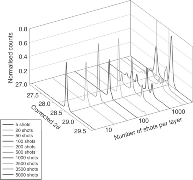
2.15 X-ray diffraction spectra for superlattices fabricated via alternating pulse bursts per target. The number of shots per burst on each target ranges from 5 to 5000 over the range of samples. The peak at 2θ = 29.74°(not shown here) corresponds to the YAG substrate and is a convenient feature for normalisation of all the XRD spectra.
For the five shot case, the appearance of a peak at a value of 2θ approximately midway between the database values for GSGG and GGG is to be expected, suggesting a truly mixed film. However, when the number of pulses per layer exceeds ~ 100, satellite peaks can be observed either side of this main central peak. These peaks are indicative of a superlattice structure (Craven et al., 2003; Ishibashi et al., 2000) and their symmetrical 2θ displacement from the central mixed peak can be used to precisely calculate the periodicity of the superlattice grown. The intensity of the central peak decreases as the number of shots per burst increases from 100 to 1000. From 2500 shots per layer onwards, the central peak is not observed, the satellite peaks become less significant and the pattern approaches that of the two individual component materials.
Observation of these satellite peaks, and more importantly their relative intensities compared to the central mixed peak are good indicators of the quality and uniformity of the layers grown. For PLD conditions that are stable, the thickness of a film deposited for 100 laser pulses, for example, can be extremely repeatable, and this is a prerequisite for the observation of such superlattice satellite peaks. Deposition runs have also been performed where the number of shots per layer has been varied from 700 to 100, in steps of 50, to fabricate a simple chirped stack, and also from 200 to 600, also in steps of 50, as shown in Fig. 2.16, but with varying numbers of total shots per section, to fabricate a compensated chirped structure so that each section has approximately the same thickness.

2.16 Diagram illustrating the number of repetitions of each layer in each component superlattice section. Layers of GGG and GSGG are represented by black and white sections respectively. The number of layer repetitions was chosen so that the overall thickness of each section is approximately equal (~ 6000 shots in total) (after Sloyan et al., 2010).
In fact, given the ease with which this shuttered PLD growth can be automated, growth of layers or stacks to any desired final design is now routine, and our next step is to fabricate designer Bragg stacks that we have modelled theoretically and are shown in Fig. 2.17. A structure consisting of 58 alternating YAG and GGG layers on a YAG substrate would theoretically result in 90% reflectivity, while 99% reflectivity could be achieved with a structure consisting of 90 layers. Such structures would have total thicknesses of ~ 8 and ~ 12.5 μm respectively, excluding substrates, a value that is easily achievable with our current PLD set-up.
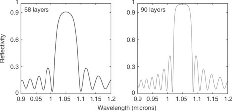
2.17 MATLAB simulations for Bragg multilayers for reflectivities of 90% (58 layers) and 99% (90 layers), using alternate YAG and GGG crystalline layers (after Sloyan et al., 2010).
2.3.5 Mixed growth: different targets with variable relative plume time delay
As a final example of the flexibility afforded by a multi-target PLD system, we show that there is the potential to further tailor material properties by varying the time delay between successive laser pulses on two different targets. These properties include the lattice constant and hence by definition the refractive index of the deposited film, a parameter of fundamental importance in the design of optical waveguides.
At first sight, the relative time delay between successive pulses might not appear to have any major effect. When using more than one plasma plume the most logical choices would be to use either simultaneous plume arrival at the substrate, in which case a mixed film would be grown, or alternating plume arrival, where the film would grow from consecutive deposition from each target. Given our previous results as shown in Section 2.3.4, however, where no evidence of any layering occurred when layer thicknesses were less than 50 shots per target (~ 1 nm thickness), and XRD spectra indicated mixed growth in all cases, the use of alternating laser pulses even with variable time delays was not expected to prove important.
The results, however, showed that for two laser plumes, the time delay can be a crucially important factor in the final film properties (Sloyan et al., 2009). For time delays of order of the transit time for one plume to reach the substrate (some ~ 100 μs for example) the second plume is travelling in the first plume’s wake, and hence does not experience the same background gas conditions such as pressure, collisional interaction and dynamic modification of the ion velocity, as would be the case if the two plumes were either synchronous or time delayed by much longer than this characteristic transit time.
In Fig. 2.18 we show a plot of the variation in film lattice constant normal to the film plane, derived from XRD spectral analysis, as a function of increasing relative delay between the two plumes that ranged from 3.2 μs to 50 ms. All delay values here took into account the relative difference in Q-switching times between the two lasers used and so are absolute delay values.
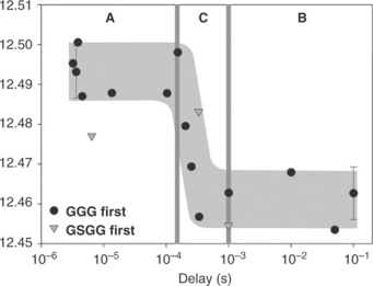
2.18 Plot of measured film lattice constant for different plume delay times. Data have been included for both plume arrival orders (GGG plume first, GSGG plume first) (after Sloyan et al., 2009).
Two distinct regions of lattice constant (A and B) may be observed, with a transition region (C) occurring between ~ 150 μs and ~ 1 ms. The exact position of this transition region appeared to vary slightly dependent on plume order, however the same overall trend was observed both in the case of the GGG plume arriving at the substrate first (followed by the GSGG plume) and vice versa. The measured lattice constant for a delay of 100 ms (i.e., completely synchronous plumes for the 10 Hz laser repetition rate used) shows the same behaviour (within experimental error) as the lattice constant for a delay of 50 ms (i.e., completely asynchronous). An ion probe positioned in place of the substrate was used to examine ion signals that occurred for single-target ablation and dual-target ablation under various relative time delays, to help elucidate the reasons behind this change in lattice constant that occurred within region C.
Analysis of these ion signals showed that for time delays of > 100 μs, the second plume was travelling in effectively a lower background gas pressure, as the first plume had swept away the gas in front of the target-probe region. For longer time delays around ~ 400 μs, the ion signal of the second plume was very similar to that of a single plume, and the partial vacuum created by the first plume had been refilled by the background gas. The time to refill this interaction region depends on several factors, but is predominantly a function of the size of the refilled region and the sound velocity in the gas. A rough estimate, however, of the time taken to refill this depleted region yields a value of 170 μs, which is consistent with the delay beyond which the ion signal of the second plume becomes gas-like again. The higher value of lattice constant for delays below ~ 200 μs may therefore be due to higher energy ion bombardment of the growing film, which can lead to in-plane compressive stress. For delays greater than 200 μs, the partial vacuum created by the first plume will be refilled and collisions with oxygen will slow down a significant fraction of the ions in the second plume.
It is interesting to note that the difference in values of lattice constant between regions A and C amounts to some 0.3%, a value that closely matches the difference between core and cladding in thin optical waveguides. The control parameter of relative time delay between plumes may therefore be a simple and controllable tool for growing a refractive index-tailored waveguide (under the assumption that refractive index is a linear function of lattice parameter).
2.4 Use of three different targets: combinatorial growth
In previous sections, we have discussed the use of PLD techniques that use multi-target geometries, but so far have only considered two targets at most. If three targets are used, then the parameter space for conducting depositions opens out still further. Shown in Fig. 2.19 is a schematic of a ternary phase diagram, where essentially any composition can be generated from three targets, A, B and C, under appropriate ablation conditions. The flexibility to grow films with specific or designer properties is therefore enormous, albeit at the experimental cost of running three lasers in place of the previous two for dual-target deposition.

2.19 Schematic of combinatorial PLD using multiple targets, here labelled A, B and C. By control of either laser fluence or laser repetition rate on each target, any film composition is accessible within this ternary phase diagram.
While we have operated our PLD system with three independent lasers and targets, so far dual beam has afforded us a wealth of growth opportunities that we are still exploring. Three laser/three target geometries can also play a role, however, when materials are deposited that require horizontal patterning. In such cases the growth rate and the area of deposition can both benefit from multiple plume geometries.
2.4.1 Horizontally patterned structures: masking and local deposition
This final section addresses the use of multiple pulses and targets to grow single-crystal structures in which there is a horizontal (in-plane) patterning from the use of masks or cones. Shown schematically in Fig. 2.20 is the underlying principle behind such horizontal patterned growth.

2.20 (a) PLD in restricted geometries: growth through a slit. (b) PLD in restricted geometries: growth through a cone.
Using either growth through a slit, as in Fig. 2.20a, or through a cone, as in Fig. 2.20b, there are the inevitable problems of diffusion or shadowing around the physical hard edge of the mask or cone, as the plasma plume will never be confined by such a physical geometry. For a mask, it can be impractical and inconvenient to fully contact to the substrate as removal after substrate heating and deposition may be difficult and lead to inevitable degradation of edge quality. The alternative of proximity coupling, using mechanical attachment can work, and we have used a thin (25 μm) Si single-crystal mask with a 2.0 mm central laser-machined circular aperture, placed over the substrate and attached via solvent capillary action. Growth through a metal cone has also been tried and results are so far satisfactory.
However, as shown in Fig. 2.21a and 2.21b for physical masking and cone growth respectively, there is an inevitable edge-shadowing effect. For some applications where a secondary overgrowth of another deposited layer is needed, the edge slope, which has been measured to be ~ 0.5°, can prove restrictive. One of our main goals is to fabricate doped thin disk lasing structures (Giesen and Speiser, 2007) with a central doped core of a few millimetres in diameter, surrounded by an undoped cladding region. Even for such a small difference in refractive index of <0.1%, such a slope region will lead to unacceptably high reflectivity for the diode pumps that will be used to pump the central doped core in a waveguide geometry. Our attention has therefore turned to a three target arrangement as shown in Fig. 2.22, which has a central doped plume deposited via a cone and two undoped plumes simultaneously depositing the cladding region.

2.21 (a) PLD growth through a 2 mm diameter laser-machined Si mask, placed in close proximity to the substrate. Notice the pronounced edge-effects around the perimeter, indicating lack of clear geometrical shadowing. (b) PLD growth through a cone of ~ 2 mm exit diameter. (photograph by Sam Berry)

2.22 Three target/three plume geometry for horizontally structured growth for thin disk laser applications.
Success here would be a major achievement, and would result in an ideal thin disk structure that can be waveguide pumped, is all single-crystal format, and has the dopant located in the central lasing region. The final benefit of this three plume arrangement is that the transition region between the undoped cladding and the doped core would be graded, over perhaps a region of ~ 1 mm, an ideal scenario to assist in Gaussian profiling of the laser mode intensity.
2.5 Future work in complex PLD geometries
Figure 2.23a and 2.23b show two generic geometries that are still high on our priority list that are fundamental to all lasing waveguide geometries: graded layers and Gaussian doping. While a graded structure would only require a dual beam set-up, and practically we have already demonstrated this capability in the chirped growth reported in Section 2.3.4, the geometry of Gaussian doping in the plane of the core with additional growth of a suitable superstrate layer does require a three target set-up, and we intend to report our results on this technique soon.

2.23 (a) Schematic of graded interface between materials A and B. (b) Schematic of Gaussian Nd concentration profile within a GGG planar waveguide structure: the final refractive index and Nd concentrations are shown for comparison.
What is certain, however, is that a multi-target, multi-beam PLD set-up is an extremely versatile and valuable piece of equipment, and will lead to many new techniques, geometries and, eventually, devices for application to a wide range of thin film materials fabrication.
2.6 Conclusions
The extension to multiple lasers and targets in PLD research has been shown to provide an important further degree of freedom. Through the judicious choice of targets and the sequence of ablation on each target as sequential, simultaneous or time-delayed, a range of complex material deposition can be achieved. Multiple laser plumes also allow for horizontally structured growth, in which millimetre scale features can be grown that are fully embedded within a dissimilar material matrix. Although few labs to date have invested in multiple beam PLD geometries, it seems that this may well become routine once the benefits and technological opportunities for thin film growth afforded by multiple plume interaction geometries are appreciated and progressively adopted.
2.7 Acknowledgements
The authors are pleased to acknowledge the contributions and collaborations that we have had in the past on PLD research and publications with the following colleagues: Steve Barrington, Sam Berry, Taj Bhutta, Christos Grivas, Steven Huband, James Lunney, Alistair Muir, Dave Shepherd, Pamela Thomas, David Walker and Michalis Zervas.
2.8 References
Barrington, S.J., Bhutta, T., Shepherd, D.P., Eason, R.W. The effect of particulate density on performance of Nd:Gd3Ga5O12 waveguide lasers grown by pulsed laser deposition. Optics Communications. 2000; 185:145–152.
Chen, L.C. Particulates generated by pulsed laser ablation. In: Chrisey D.B., Hubler G.K., eds. Pulsed laser deposition of thin films. New York: John Wiley; 1994:167–198.
Craven, M.D., Waltereit, P., Wu, F., Speck, J.S., DenBaars, S.P. Characterization of a-plane GaN/(Al,Ga)N multiple quantum wells grown via metalorganic chemical vapor deposition. Japanese Journal of Applied Physics. 2003; 42:235–238.
Darby, M.S.B., May-Smith, T.C., Eason, R.W. Deposition and stoichiometry control of Nd-doped gadolinium gallium garnet thin films by combinatorial pulsed laser deposition using two targets of Nd:Gd3Ga5O12 and Ga2O3. Applied Physics A: Materials Science and Processing. 2008; 93:477–481.
Dijkkamp, D., Venkatesan, T., Wu, X.D., Shaheen, S.A., Jisrawi, N., Min-Lee, Y.H., McLean, W.L., Croft, M. Preparation of Y-Ba-Cu oxide superconductor thin films using pulsed laser evaporation from high Tc bulk material. Applied Physics Letters. 1987; 51:619–621.
Eason R.W., ed. Pulsed laser deposition of thin films: Applications-led growth of functional materials. Hoboken, NJ: John Wiley, 2007.
Eason, R.W., May-Smith, T.C., Grivas, C., Darby, M.S.B., Shepherd, D.P., Gazia, R. Current state-of-the-art of pulsed laser deposition of optical waveguide structures: existing capabilities and future trends. Applied Surface Science. 2009; 255:5199–5205.
Gamaly, E.G., Rode, A.V., Luther-Davies, B. Ultrafast laser ablation and film deposition. In: Eason R.W., ed. Pulsed laser deposition of thin films: Applications-led growth of functional materials. Hoboken, NJ: John Wiley; 2007:99–130.
Gaponov, S.V., Gudkov, A.A., Fraerman, A.A. Processes occurring in an erosion plasma during laser vacuum deposition of films. III. Condensation in gas flows during laser vapourization of materials. Soviet Physics – Technical Physics. 1982; 27:1130–1133.
Gazia, R., May-Smith, T.C., Eason, R.W. Growth of a hybrid garnet crystal multilayer structure by combinatorial pulsed laser deposition. Journal of Crystal Growth. 2008; 310:3848–3853.
Giesen, A., Speiser, L. Fifteen years of work on thin-disk lasers: Results and scaling laws. IEEE Journal of Selected Topics in Quantum Electronics. 2007; 13:598–609.
Gorbunoff, A. Cross-beam PLD: Metastable film structures from intersecting plumes. In: Eason R.W., ed. Pulsed laser deposition of thin films: Applications-led growth of functional materials. Hoboken, NJ: John Wiley; 2007:131–160.
Grivas, C., May-Smith, T.C., Shepherd, D.P., Eason, R.W. Laser operation of a low loss (0.1 dB/cm) Nd:Gd3Ga5O12 thick (40 μm) planar waveguide grown by pulsed laser deposition. Optics Communications. 2004; 229:355–361.
György, E., Sauthier, G., Figueras, A., Giannoudakos, A., Kompitsas, M., Mihailescu, I.N. Growth of Au-TiO2 nanocomposite thin films by a dual-laser, dual target system. Journal of Applied Physics. 2006; 100:114302–114305.
Ishibashi, Y., Ohashi, N., Tsurumi, T. Structural refinement of X-ray diffraction profile for artificial superlattices. Japanese Journal of Applied Physics. 2000; 39:186–191.
Kompitsas, M., Giannoudakos, A., György, E., Sauthier, G., Figueras, A., Mihailescu, I.N. Growth of metal-oxide semiconductor nanocomposite thin films by duallaser, dual target deposition system. Thin Solid Films. 2007; 515:8582–8585.
May-Smith, T.C., Eason, R.W. Comparative growth study of garnet crystal films fabricated by pulsed laser deposition. Journal of Crystal Growth. 2007; 308:382–391.
May-Smith, T.C., Grivas, C., Shepherd, D.P., Eason, R.W., Healy, M.J.F. Thick film growth of high optical quality low loss (0.1 dB cm−1) Nd:Gd3Ga5O12 on Y3Al5O12 by pulsed laser deposition. Applied Surface Science. 2004; 223:361–371.
May-Smith, T.C., Muir, A.C., Darby, M.S.B., Eason, R.W. Design and performance of a ZnSe tetra-prism for homogeneous substrate heating using a CO2 laser for pulsed laser deposition experiments. Applied Optics. 2007; 47:1767–1780.
May-Smith, T.C., Shepherd, D.P., Eason, R.W. Growth of a multilayer garnet crystal double-clad waveguide structure by pulsed laser deposition. Thin Solid Films. 2007; 515:7971–7975.
May-Smith, T.C., Sloyan, K.A., Gazia, R., Eason, R.W. Stress engineering and optimization of thick garnet films grown by pulsed laser deposition. Crystal Growth & Design. 2011; 11(4):1098–1108.
Sloyan, K.A., May-Smith, T.C., Eason, R.W., Lunney, J.G. The effect of relative plasma plume delay on the properties of complex oxide films grown by multilaser, multi-target combinatorial pulsed laser deposition. Applied Surface Science. 2009; 255:9066–9070.
Sloyan, K.A., May-Smith, T.C., Zervas, M., Eason, R.W., Huband, S., Walker, D., Thomas, P. Growth of crystalline garnet mixed films, superlattices and multilayers for optical applications via shuttered combinatorial pulsed laser deposition. Optics Express. 2010; 18:24679–24687.
Tomashpolskii, Y.Y., Sevostianov, M.A. Epitaxial ferroelectric films. Ferroelectrics. 1980; 29:87–90.
Wang, S.Z., Xiong, G.C., He, Y.M., Luo, B., Su, W., Yao, S.D. High misfit epitaxial growth: superconducting YBa2Cu3O7–x thin films on (100)BaF2 substrates. Applied Physics Letters. 1991; 59:1509–1511.
Yoshitake, T., Nagayama, K. The velocity distribution of droplets ejected from Fe and Si targets by pulsed laser ablation in a vacuum and their elimination using a vane-type velocity filter. Vacuum. 2004; 74:515–520.