6
Gate All Around MOSFETs-A Futuristic Approach
Ritu Yadav1* and Kiran Ahuja2
1 ECE Department, IK Gujaral Punjab Technical University, Jalandhar, India
2 ECE Department, DAVIET, Jalandhar, India
Abstract
In this chapter, the history of semiconductor technology and its continuous development processes such as recent MOSFET technologies, the significance of scaling in CMOS technology, challenges in scaling, futuristic scaling method (technology booster) the introduction of high-K, circuit design, and device modeling techniques are discussed. Considering all these challenges in the current scenario, this study was undertaken with the key focus on reducing the leakage current, improv- ing the subthreshold slope, and developing immunity against the short channel effect by introducing the hetero di-electric oxide (combination of high-K (HfO2 and TiO2) and traditional SiO2) in triple asymmetric metal gate by quantization approach. Advance multiple devices such as Gate-all-around can be effectively used to improve the performance of the device in terms of the chip design area, speed, and power by using work function engineering and dielectric engineering. The quantum effect on the gate-all-around device is also discussed in detail.
Keywords: Gate-all-around (GAA), Sub-threshold voltage (SV), DIBL, SCEs
6.1 Introduction
VLSI (very large-scale integration) is an advanced and emerging field in the semiconductor industry for circuit implantation, system-level design, and memory applications. In the current scenario, when the usage of electronics in the fields of automation, information technology, wireless, and telecommunication has been increasing day by day, then it becomes nec- essary to evolve such a technology that can make semiconductor chips smaller and lighter in weight, energy-efficient, with larger data handling, faster response time, and capable of sustaining the resources. This can be achieved by applying VLSI design techniques using ultra-small sizes with high integration density and low power consumption with enhanced performance, which is possible by using nano-scale technology by introducing new materials.
6.1.1 Semiconductor Technology: History
Before the 21st century, electronics fabrication was dependent on vacuumtube technology. The key point in semiconductor history was the introduction of MOSFET by Lilienfeld [1, 2] in 1930, which replaced the vacuum-tube based with novel compact dimension semiconductor transistor technology, as shown in Figure 6.1(a,b). The author claimed that the proposed device used copper-sulfide semiconductor material three-electrode structure. However, fabrication feasibility was not possible in working devices. This concept was famous for the field-effect transistor. The p-n junction in 1940 [3] was discovered by the Ohl’s serendipitous, and later, in 1948, W. Shockley developed a p-n junction-based transistor [4].
When in 1948 Shockley discovered the first transistor (BJT), he set a milestone in solid-state electronics. Compared to vacuum-tube technology, the BJT was more reliable and less power-consuming, but the fabrication approach was complex. Therefore, even with the amazing capabilities, the feasibilities of this novel technology required miniaturization to reduce the cost of the elements. Further enhancement in the performance of the VLSI the computer industry developed a MOSFET. In 1950 the first electronics computer was introduced, which was based on vacuum-tube technology, and thereafter various inventions were also made by using this technology. The use of vacuum was weak and this technology became nonexistent because of complex circuit design. This device became the most popular in the electronics industry in the form of the rectifier and became a major component in the design of semiconductor devices. In 1951 Bell Laboratories [4, 5] successfully manufactured the first bipolar junction-based transistor. In 1958, Jack Kilby at Texas Instruments envisaged the thought of the (IC) and. Robert Noyce made the IC [6], as depicted in Figure 6.1(b). Richard Feynman in 1959 delivered a speech in which he said that the performance of the device may be enhanced by scaling down of devices. In 1959 Noyce developed a patent for the IC and with the help of this made multiple components on a single piece of silicon.

Figure 6.1 Traditional device structure of N-channel MOSFET and energy band. (b) First-IC fabricated by Jay Last [11].
Two years later, in 1960, Atalla and Kahng constructed a MOSFET device based on silicon substrate by using SiO2 as a dielectric [7], which was at that time widely used in the implantation of circuits design. Thereafter, the first commercial device was introduced by Texas Instruments and named 502 Binary Flip-Flop. In the following year, 1961, the “fully-integrated circuit” family was introduced [8].
After two years, the CMOS was invented [9, 10], which replaced the design structure from a few transistors with billions of transistors as shown in Figure 6.2. By Moore’s law [12], transistors increase every year which enhances the packing density of transistors on a chip.
After that, in 1975, this concept was revised with the declaration that the number of transistors would be increased per year [13, 14]. This forecast is famously known as Moore’s law and is applied as a ruling in the VLSI area. In 1971 the first microprocessor was developed by Ted Hoff and Stanley Mazor [15] and one of the popularly known ones was Intel’s 4004.

Figure 6.2 Increased numbers of transistors per year [17].
The first commercial microprocessor enclosed 2300 transistors in a 16-pin IC of Intel, which introduced microprocessors accommodating above multi-billion transistors on a chip [1]. I.R. Committee [16, 17] pre-sented the idea of scaling down devices by following the direction of the ITRS. However, this prediction had been implanted for three decades. Then transistor logic family [18] commenced the first microprocessor in 1972 which enclosed above two thousand pMOS transistors. As the growth of transistors increased exponentially according to Moore’s law, other micro-processors were introduced based on nMOS technology but consumed more power due to the increased number of transistors per chip.
The latest technology required, like CPU can contain two billion transis- tors; however, CMOS technology is still the basic structural element of the circuitry for logic integrated circuits. Unfortunately, even the most innovative solution is CMOS technology which follows the scaling law. GPU processor-based Itanium-7quad contains 1.1 billion; this is possible with the help of scaling law. Scaling law defines shrinking the size of a device such that to acquire a smaller chip area while balancing the characteristics of MOSFETs.
6.2 Importance of Scaling in CMOS Technology
Downscaling of transistors improves the design structure of the device, improves the performance of the device, and reduces the cost. Dennard and fellow researchers in 1972 [19] proposed the scaling schemes. With the help of the same scaling factor, it can scale the device dimensions vertically and horizontally, hence it avoids the short channel effect (SCEs) and increases electrostatics controllability in the fabrication of smaller devices by the scaling factor. The main features of downscaling are the significant reduction in device dimensions, higher packing density, and dynamic power saving through lesser voltage, performance improvement and cost reduction.
In the latest scenario, with the help of scaling Itanium-7 quad-core GPU processor which contains 1.1 billion transistors and Intel 32nm static ran- dom access memory (SRAM) has about 800 billion transistors.
6.2.1 Scaling Rules
Leakage current is the major challenge in semiconductor CMOS technology. The literature survey reveals that shrinking the size of the gate length and oxide thickness decreased by scaling factor of 102, then biasing voltage reduced and packing density increased only by factor 10, power consumption increased by 105. The Semiconductor Industry Association (SIA) expects to achieve the 10 nm technology for the same various set of rules illustrated in Table 6.1.
| Microelectronics parameters | Scaling factor | Limiting factors | Resolution |
|---|---|---|---|
| Voltage Vdd | 1/â | Thermal Voltage | Low operating temp. |
| Electric Field | I | - | - |
| Channel Length L | 1/â | Lithography | Multiple gate structure follow gate engineering |
| Drain Current | 1/â | Punch through | |
| Gate capacitance per unit area, Cox = εox/D | Â | Leakage current | Oxynitride |
| Gate area, Ag = L × W | 1/â2 | ||
| Gate capacitance Cg = εoA/d | 1/â | ||
| Parasitic capacitance Cx | 1/â | ||
| Carrier density in channel, Qon = Co Vgs Channel resistance Ron =1/WQon | 1 1 | - | High mobility material/ strained devices/ Chemical process |
| Gate propagation delay Tpd | 1/â | Non-Scalable Vdd | |
| Maximum operating frequency, fo | â2 | Parasitic capacitance | Low K-insulator Copper wire |
| Saturation current, Idss | 1/â | Gate leakage current | Efficient power management High - k-dielectric |
| Current density, J | Â | ||
| Switching energy per gate Eg = I Cg (VDD) 2/2 | 1/â3 | ||
| Power dissipation per gate, PgPg = Pgs + Pgd Both Pgs and Pgd are scaled by | 1/â2 | ||
| Power speed product, PT = Pg Td | 1/â3 | ||
| Transistor per chip | â2 | Complexity in interconnection | Serial signal communication |
The gate length thickness reduces by a scaling factor of 1/â, then oper- ating voltage may be reduced by 1/â, and the circuit delay is reduced by 1/â. Consequently, there is degradation of the device characteristics and performance. So the forthcoming devices may be related to lower technology nodes [20]; have proposed finding alternatives to the consequences that occurred during downscaling of device size known as scaling rules for CMOS technology.
6.2.2 The End of Planar Scaling
The device miniaturizing happens through the process of scaling. The channel length is estimated to be 10 nm or below according to the 20 nm technology node [21]. The effect of scaling results in various SCEs such as degraded threshold-voltage, DIBL, subthreshold slope.
In the new millennium scaling came to an end because further, it was not possible to assure better electrostatic control of transistors, mainly because SCEs degraded the performance [22].
Short channels such as mobility degradation, named surface scattering, occurred by increasing the gate voltage in the channel region. Other effects are depletion capacitance and gate capacitance and these arose by increasing the EOT and therefore reducing the current of the device. The sub-threshold-swing should be closest to the ideal value (60mV/decade). Parasitic resistance effects were raised due to the down scaling of the channel length and the increased S/D (source to drain) resistances. Leakage current and GIDL (gate induced drain lowering) and hot-carrier effects arise due to ultra-scaling gate-oxide-thickness. Threshold voltage roll-off arises with scaling gate length. DIBL effects degraded the threshold voltage by increasing drain voltage. Continuous scaling of silicon-based substrate transistors provides better performance and reduces the thermal power budget. There is an emerging requirement, that demands continued scaling in various applications like data centers, memory banks, etc.
International Roadmap for Device and Systems (IRDS) predicted that after 2027 there will be no space for further downscaling of the device, because due to ultra-scaling some undesired issues arise in the device, such as gate tunneling, increasing the OFF current, and deteriorating the performance of the device.
6.2.3 Enhance Power Efficiency
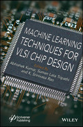
Figure 6.3 illustrates the total power dissipation with respect to technology node.
Figure 6.3 Total power dissipation with technology node [31].
This gap shows the requirement to control at the device level. The power requirement is estimated through equation 1.1 [23].
In this equation PD and PS are the static and dynamic power dissipation, α is the scaling factor and CL is the capacitance-load, VDD is the drain-voltage which is lower than the power requirement is also lower, ILeakage and Ith are the total leakage current and threshold current, Vth is the minimum gate voltage if higher the threshold voltage lower the power consumption and SS is the subthreshold swing.
Some short channel effects such as gate tunneling scattering and quantum effect are provoked by reduction of gate oxide thickness, silicon thickness and doping concentration. To trade-off between power consumption and short channel effect (SCEs) the device required a substitute structure and architecture to keep on advanced CMOS scaling [24].
6.2.4 Scaling Challenges
Various types of scaling challenges are categorized mainly into two types, horizontal and vertical [25]. If shorter the Lg then degrades the threshold voltage, SCEs appeared under influence of higher drain voltage (Vds). In the ULSI (ultra-large-scale integration) industry gate length is represented by Lg, where L is the characteristic length defined in the equation
These metrics such as oxide-thickness (tox), junction depletion width (Xj), and total depletion width (T2dep) must be vertically shrunk along with channel length (Lg) to reduce SCEs in bulk MOSFETs. There are the following effects because of vertical scaling in the device.
6.2.4.1 Poly Silicon Depletion Effect
Scaling of oxide leads to degradation of gate capacitance and transconductance and also increases the poly-deflection layer in the inversion mode. The deflection region cannot be reduced due to the limitation of doping (1019, 1020 cm-3). The result of this effect is in terms of shifting of the threshold voltage. This challenge can be avoided by using a metal gate.
6.2.4.2 Quantum Effect
Electric field increases near silicon/oxide interface due to downscaling of the oxide thickness. It creates quantum confinements of the carrier which lead to increased discrete sub-band and shifts the charge carrier from the interface.
6.2.4.3 Gate Tunneling
The use of the direct and Fowler Nordheim method of downscaling oxide thickness increased the static power dissipation. Employing high-k (HfO2 and Si3N4) reduces this effect.
6.2.5 Horizontal Scaling Challenges
In this lateral scaling, there is only scaling, of channel length (gate length) named as “Gate shrinking” which raised SCEs. There are the following horizontal scaling challenges.
6.2.5.1 Threshold Voltage Roll-Off
Threshold roll-off becomes extra impressive by the increased drain voltage. During scaling of channel length then depletion width becomes large than the channel length. Then channel barrier height reduces, which is manifested as threshold roll-off and DIBL.
6.2.5.2 Drain Induce Barrier Lowering (DIBL)
DIBL effects occur when source to channel barrier height is reduced by increasing the electrical field with high drain voltage. If there are decreases in the height of the barrier from source to channel then the carriers are without restraint inserted in the channel region. Therefore, the threshold voltage lower gate loses control over the channel. DIBL is also named the “charge sharing model”. It is managed by the gate. The threshold voltage is calculated by the total depletion charge.
Q'd, Qd, ΔQ are the depletion-charge in the gate region, total-depletion and depletion-charge in drain region Vfb flat-band voltage, Vth threshold voltage.
6.2.5.3 Trap Charge Carrier
The large electric field in the device produces a hot carrier (electrons) which has sufficiently high energy and momentum to inject the oxide and trap the Si/oxide interface; it causes the breaking of the Si-H band inter-face. Hot-carrier effects reduce the reliability of the device, increase the SCEs, decrease the Vth and increase the drive-current.
6.2.5.4 Mobility Degradation
Continuous miniaturization of the device requires more amount of channel doping concentration because it balances the electric field in the channel area. Higher doping concentrations avoid mobility scattering. Higher amount doping concentration creates dopant fluctuation inside the channel which results in mobility scattering and mobility roughness.
6.3 Remedies of Scaling Challenges
To overcome all these undesired SCEs, it is essential to increase the performance with novel technology boosters. Surface scattering can be enhanced by using various materials such as Germanium, Si-Ge or III-V compounds; these materials have better electron and hole mobility than silicon. Further, strain technology is most widely used to improve mobility.
By inserting high-k dielectrics gate capacitance is improved. Parasitic effects improved, OFF-current can be reduced by the implementing of silicon on insulator (SOI) layers, instead of bulk transistors.
However, even in multiple-gate MOSFETs, the reduced size of the device vertically and horizontally would be affected by SCEs [26, 27]. To reduce these effects, it is necessary to add together novel gate engineering and dielectric engineering [28–30] in the device structure.
6.3.1 By Channel Engineering (Horizontal)
By using the channel engineering technique in a multi-gate device structure the threshold-voltage increases and reduced SCEs in the device.
6.3.1.1 Shallow S/D Junction
This junction balances the space between the source and drain and maintained barrier height. In this way, the transport charge carrier movement from source to channel is less, compared to the deep shallow junction.
6.3.1.2 Multi-Material Gate
This is a very important method to reduce the hot-carrier effects. The multi-material gates combine gate architecture by two or more metals with dissimilar work function. The double and triple material gate were proposed by [32, 33] in 2008, which was based on the combination of two or three metal gates and with work-function in the source-side gate (M1) greater as compared to the drain-side gate (M2). This is due to the increased gate transport efficiency by increasing the electric field in the channel region [34] which reduces the hot-carrier effect in the dual metal gate (DMG) which is based on SOI MOSFETs.
6.3.2 By Gate Engineering (Vertical)
By employed gate-engineering in multi-gate structure [35], which is control the carrier by the gate in the channel region.
6.3.2.1 High-K Dielectric
To maintain EOT and continuous scaling the high-K was introduced by Intel in 2007 in 45nm CMOS technology. It replaces traditional oxide (SiO2) with high–K (HFO2 dielectric strength above 50).
6.3.2.2 Metal Gate
It improves the gate leakage problem in the CMOS technology gate stack employed by a combination of poly-Si/High-K. However, an experimental result shows mobility degradation by using a metal gate.
6.3.2.3 Multiple Gate
Fully depleted (FD) based on SOI MOSFET is a promising candidate to continue scaling; using this device enhances the transconductance, lowers Vth-roll-off and decreases the parasitic-capacitance, subthreshold-slope as compared to bulk MOSFETs. The incorporation of buried oxide (BOX) improves leakage current, and SCEs. However, using ultra scaling source/ drain (S/D) region FD-MOSFET required high resistance, therefore to avoid the FIBL effects from the drain channel region it requires a special gate structure.
Various emerging devices are DG, triple-gate, FINFET gate, Quantum-wire, and FD-MOSFETs [36]. The circular, rectangular and quadruple gate-like gate-all-around [37], in FD-MOSFETs using buried oxide prevents encroachment EF lines in gate region which reduces the SCEs. But in this approach, it is not appropriate to increase the junction capacitance and body effects. The various gates such as double gate, the triple gate is the most promising device operated in enhancement and depletion mode. These devices are capable to face current challenges such as power consumption crises, control SCEs, and reduction of leakage current.
The GAA MOSFETs is one of the most potential candidates with better gate controllability and energy efficiency [38]. The gate-all-around offers characteristics length more scalability than double gate; the reason behind that gate covered all sides to channel and control transport carriers in the channel area. The device size below 25 nm provided the highest current drive capability due to current flow across the surface of the silicon body, so due to this reason ON –state drive mostly double than double gate device and strong confinement of electric field because the channel is surrounded by the gate. Switching characteristics and higher ON/OFF current ratio are better than traditional MOSFET. The subthreshold swing of GAA MOSFET is near to the ideal value at room temperature which enhances switching characteristics.
6.4 Role of High-K in CMOS Miniaturization
A high-K material having a dielectric constant greater than the SiO2 is considered in the device design. The further miniaturization of microelectronic components is possible through the implementation of high-K strategy [39–41]. For the continuous process of downscaling of the transistor, the thickness of SiO2 gate dielectric needs to be decreased.
However, decrease in SiO2 thickness increases the capacitance and degrades the device performance. As ultra-scaling below 2-3 nm, leakage current increases drastically, which is named “gate tunneling”, which leads to increased static power and reduced reliability of the device [42, 43].
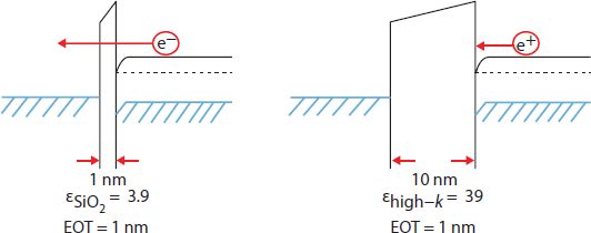
Figure 6.4 Effective oxide thickness (EOT) for high-K and conventional dielectric material [45].
Keeping in view the leakage current, the device requires high-K dielec- tric along with SiO2, so it is necessary to investigate the combination of high-K/TiO2 material along with SiO2 required for fabrication of the futur- istic CMOS devices. Undoubtedly, Si-MOSFET with high-K may be the capable candidate for future generation devices, due to its higher dielectric constant than traditional SiO2, as shown in Figure 6.4.
As per the prediction of Moore’s Law, for continuing scaling of device advanced gate material is required instead of conventional dielectric material by following the main procedure for selecting substitute dielectric oxide are permittivity, di-electric strength, valence band offset, silicon process and crystal structure.
Other high-K materials [44] are Al2O3, HfO2, TiO2, La2O3, etc. But all of these materials are thermodynamically unstable, have high breakdown voltage, low defect density, low deposition temperature, and low charge states on silicon.
The combination of high-K/TiO2 dielectric material along with SiO2 must having more superior features in comparison to the high-K value [45].
A comparison has been made on the recently used high-K materials, i.e., SiO2, HfO2, Al2O3 and TiO2 in terms of structural and physical characteristics [46–51]. The high-K materials have better features in terms of the high-K, lower band-gap, and compatibility with silicon, so it is considered a potential candidate for MOS gate dielectric applications, as depicted in Table 6.2.
Table 6.2 Comparative analysis of traditional and high-K materials [46–51].
| Di-electrical material | Di-electric strength (K) | Band-gap (Eg) (eV) | Conduction- band- offset ΔEc (eV) | Valence-band-offset ΔEv (eV) | Stability with Si | Crystal-structure |
|---|---|---|---|---|---|---|
| Silicon-dioxide (Si-O2) | 3.9 | 8.9 | 3.5 | 4.4 | Yes | Amorphous |
| Aluminum oxide (Al2O3) | 9.0 | 8.7 | 2.8 | 4.9 | Yes | Amorphous |
| Hafnia oxide (HfO2) | 25 | 5.7 | 1.5 | 3.4 | Yes | Monoclinic, cubic, tetragonal |
| Titanium oxide (TiO2) | 80 | 3.5 | 1.2 | 1.2 | Yes | Tetragonal |
6.5 Current Mosfet Technologies
The main challenges in recent semiconductor research are reduced power consumption, higher packing density, better scalability, balance leakage current, the large storage capacity of memories, and higher speed. The operational failures can be avoided by reducing the power consumption, which arises mainly due to the self-heating problem, which is fixed by the ITRS [52, 53]; further to enhance the performance of the devices the dimensions of the MOSFET are continuously decreasing. Following the novel device, such as the DG, the TG and the QGMOSFETs [54–57].
6.6 Conclusion
In this chapter, the key objective is to discuss a novel device based on nanoscale single and multi-asymmetrical hetero di-electric oxide gate-all- around nanowire for low power standby memory and sensor applications. This model is further suitable for circuit implementation. In this chapter the history of semiconductor technology and its continuous development processes such as recent MOSFET technologies, the significance of scaling in CMOS technology, challenges in scaling, futuristic scaling method (technology booster), introducing the high-K, circuit design, and device modeling techniques are discussed.
References
- 1. Intel; Intel Technology Road Map, http://www.intel.com accessed on 01/01/2020.
- 2. Lilienfeld, J. E., Method and Apparatus for Controlling Electric Currents. US Patent US1745175A. 1930, New York, NY, USA.
- 3. Shaff, J. H. (1947). Development of Silicon Crystal Rectifiers for Microwave Radar Receivers. Bell System Technical Journal, XXVI(1), pp. 1-30.
- 4. Shockley. W (1948). Circuit Element Utilizing Semiconductor Material. US Patent US2681993A. New York, NY, USA.
- 5. Shockley, W. (1949). The Theory of P-N Junctions in Semiconductors and P-N Junction Transistors. Bell System Technical Journal. 28(3), pp. 435-489.
- 6. Kilby. J. S. (1976). Invention of the Integrated Circuit. IEEE Transactions on Electron Devices. 23(7), pp. 648–654.
- 7. Atalla, M. M. J., Kahng. D. (1963). Electric Field Controlled Semiconductor Device. U.S. Patent 3102230. New York, NY, USA.
- 8. Tsvedos, T.J. (1961). Introduction to Microsystems and the RCA Micromodule. The RCA Micromodule Program: Components and Application, AIEE Electronics Division, Los Angeles, Symposium, Los Angeles, California. pp. 3.
- 9. Wanlass F., Sah, C. (1963). Nanowatt Logic Using Field-Effect Metal-Oxide Semiconductor Triodes. In Solid-State Circuits Conference. Digest of Technical Papers. VI, pp. 32–33.
- 10. Wanlass, F. M. (1967). Low Stand-By Power Complementary Field Effect Circuitry. US Patent US3356858A. New York, NY, USA.
- 11. Last, J. (2020). First Planar Integrated Circuit Is Fabricated. https://computerhistory.org
- 12. Moore, G. (1975), Progress in Digital Integrated Electronics. In Electron Devices, 21, pp.11-13.
- 13. Moore, G. (1965). Cramming More Components on to Integrated Circuits. Solid-State Electronics. 38, pp. 114-117.
- 14. Moore, G. (1929). Understanding Moore’s Law: The Future of Integrated Electronics. Chemical Heritage Press. pp. 37-55.
- 15. Faggin, F., Hoff. J., M. E., Mazor, S. (1996). The History of the 4004. IEEE Micro.16(6), pp. 10–20.
- 16. I. R. Committee et al. (2007). International Technology Roadmap for Semiconductors.
- 17. International Technology Roadmap for Semiconductors, (SIA) (2003). http://public.itrs.net, SEMATECH, edition of ITRS.
- 18. Rabaey, J. M., (2003). Digital Integrated Circuits. Pearson Education Inc. 2nd edition, 07458.
- 19. Dennard, N. (1972). Design of Micron MOS Switching Devices. IEDM Tech. pp. 168-170.
- 20. Westlinder, J., Investigation of Novel Metal Gate and High?K Dielectric Material for CMOS Technologies. Doctoral Thesis, Department of Engineering Sciences, Uppsala University, SE-75105.
- 21. Skotnicki, T., Hutchby, J.A. (2005). The end of CMOS scaling toward the introduction of new materials and structural changes to improve MOSFET performance. IEEE Dev. 21 (1), pp. 16-26.
- 22. Chang, L., Choi, Y.C.Y. (2003). Extremely scaled silicon nano CMOS devices. IEEE, 91 (11), pp. 1860-1873.
- 23. Wang X. (2010). Simulation Study of Scaling Design Performance Characterization, Statistical Variability and Reliability of Decananometer MOSFETs. Doctoral Thesis, Department of Electronics and Electrical Engineering, University of Glasgow, G12 8QQ, Scotland.
- 24. Ferain, I., Colinge, C.A., Colinge, J. (2011). Multigate Transistor as the Future of Classical Metal Gate Oxide Semiconductor Field-Effect Transistors. Nature, 479, pp. 310-06.
- 25. Nowak, E.J. (2002). Maintaining the Benefit of CMOS Scaling When Scaling Bogs Down. IBM Journal of R&D, 46(2), pp. 169-180.
- 26. Gautam, R., Saxena, M. (2013). Gate All Around MOSFET with Vacuum Gate Dielectric for Improved Hot Carrier Reliability and RF Performance. IEEE Trans Electron Dev. 60(6), pp. 1820–1827.
- 27. Rahou, F. Z. (2016). Performance Improvement of Pi-Gate SOI MOSFET Transistor Using High-K Dielectric with Metal Gate. IETE Journal. 62(3), pp. 331-338.
- 28. Narula, V. (2019). Enhanced Performance of Double Gate Junctionless Field Effect Transistor by Employing Rectangular Core-Shell Architecture. Semiconductor Science and Technology. 34(10), pp. 1-11.
- 29. Zhang, J. W. (2014). Microstructure Optimization and Optical and Interfacial Properties Modulation of Sputtering-Derived Hfo2 Thin Films by Tio2 Incorporation. Journal of alloys and Compounds. 611, pp. 253-259.
- 30. Zhou, X., Long, W. (1998). A novel hetero-material gate (HMG) MOSFET for deep-submicron ULSI technology. IEEE Trans. Elec. Device. 45, pp. 2546-2548.
- 31. Mudge T. (2001). Power: A First-Class Architect Design Constraint. IEEE Computer. 34, pp. 52-58.
- 32. Long W. (1999). Dual Material Gate (DMG) Field Effect Transistors. IEEE Trans. on Electron Devices, 46(5), pp. 865-870.
- 33. Orouji, A. (2008). Nanoscale Triple Material Double Gate (TM-DG) MOSFET for Improving Short Channel Effects. International Conference on Advances in Electronics and Micro-Electronics, Valencia, Spain, IEEE Proceedings. pp. 11-14.
- 34. Jin, L. (2010). Two Dimensional Threshold Voltage Analytical Model of DMG Strained –Silicon on Insulator MOSFETS. Journal of Semiconductors. 31(8), pp. 084008(1-6).
- 35. Kumar M., Haldar S. (2014). Impact of Gate Material Engineering on Analog/ RF Performance of Nanowire Schottky Barrier Gate All Around MOSFET for Low Power Wireless Applications. Microelectronics Journal. 45(11), pp. 1508-14.
- 36. Tiwari P.K., Dubey S. (2010). A two-dimensional analytical model for threshold voltage of short-channel triple-material double-gate metal-oxide-semiconductor field-effect transistors. J. Appl. Phys. 108, 074508.
- 37. Fahad, H.M., Smith, C.E. (2011). Silicon Nanotube-Field-Effect Transistor with Core-Shell Gate Stacks for Enhanced High Performance Operation and Area Scaling Benefits. Nano Lett. 11 pp. 4393-4399.
- 38. Pratap Y., Ghosh P., Haldar S. (2014). An Analytical Subthreshold Current Modelling of Cylindrical Gate All Around (CGAA) MOSFET Incorporating the Influence of Device Design Engineering. Microelectron Journal. 45, pp. 408-415.
- 39. Gang, H., Deng B. (2013). Effect of Dimethyl Aluminium Hydride-Derived Aluminum Oxynitride Passivation Layer on the Interface Chemistry and Band Alignment of Hftio-Ingaas Gate Stacks. APL Materials. 1(1).
- 40. Chen, F. (2004). A Study of Mixtures of Hfo2 and Tio2 as High-K Gate Dilectrics. Microelectron Eng. 72, pp. 263-266.
- 41. Bera M.K., Maiti, C.K. (2006). Electrical Properties of Sio2/Tio2 High-Κ Gate Dielectric Stack. Materials Science in Semiconductor. 9, pp. 909-917.
- 42. Cho, K. (2002). First Principles Modeling of High–K Gate Dielectric Materials. Computational Materials Science. 23, pp. 43.
- 43. Chau, R. (2004). High-/Metal– Gate Stack Andits MOSFET Characteristics. IEEE Electron Device Letter. 25, pp. 408.
- 44. Chui, C.O. (2002). A sub 400o C Germanium MOSFET Technology with High-k Dielectric and Metal Gate. IEDM Tech. Dig. 8–11, pp. 437.
- 45. Iwai, H., Wong, H. (2006). On the Scaling Issues and High-K Replacement of Ultrathin Gate Dielectrics for Nanoscale MOS Transistors. Microelectronics Engg. 83, pp. 1867-1904.
- 46. Buchanan, D.A. (2000). 80nm Poly-Silicon Gated N-FETWith Ultra-Thin Al2O3 Gate Dielectrics for ULSI Applications. IEDM Tech Digest. pp. 223-226.
- 47. Perkins, C.M. (2002). Thermal Stability of Polycrystalline Silicon Electrodes on Zro2. Appl. Phys. Lett. 81, pp. 1417-1419.
- 48. Dalapati, G.K. (2003). Electrical Properties of Ultrathin Tio2 Films on Si1Ycy Hetero Layers. Solid-State Electronics. 47(10), pp. 1793–1798.
- 49. Gusev, E.P. (2003). Ultrathin Hfo2films Grown on Silicon by Atomic Layer Deposition for Advanced Gate Dielectrics Applications. Microelectronic Engineering. 69(24), pp. 145-151.
- 50. Choudhary, P. (2008). The Structural and Electrical Properties of Tio2 Thin Films Prepared by Thermal Oxidation. Condensed Matter. 403(19), pp. 3718-3723.
- 51. 2012. International Technology Roadmap for Semiconductors (ITRS).
- 52. Arora, N. (2017). MOSFET Models for VLSI Simulation. WorldScientificPublishing.596224.
- 53. Iniguez, B. (2006). Compact-Modeling Solutions for Nanoscale Double-Gate and Gate-All-Around MOSFETs. IEEE Transactions. 53(9), pp. 2128–2142.
- 54. Colinge, J.P. (1990). Silicon-Insulator ’Gate-All-Around Device. Electron Devices Meeting IEDM, pp.595–598.
- 55. Colinge, J.P. (2007). Multiple-Gate SOI MOSFETS. Solid-State Electronics. 48, pp. 897–905.
- 56. Mendiratta, N., Tripathi, S.L. & Chander, S. Analytical Model of Dopingless Asymmetrical Junctionless Double Gate MOSFET. Silicon (2022). https://doi.org/10.1007/s12633-022-01819-z
- 57. Verma, S., Tripathi, S.L. Impact & Analysis of Inverted-T Shaped Fin on the Performance Parameters of 14-nm Heterojunction FinFET. Silicon (2022). https://doi.org/10.1007/s12633-022-01708-5
Note
- * Corresponding author: [email protected]