
7
Three‐Phase Transformers
Three‐phase transformers come in many sizes and are found throughout the power system. Many are designed and built for specific applications, like the transmission transformer in Figure 7.1a, while others are ‘off the shelf’ designs, used in many standard distribution applications. The small resin cast transformer shown in Figure 7.1b is an example of such a transformer; it finds application in interior substations where the risk of fire and spillage from oil‐insulated transformers is to be avoided.


Figure 7.1 (a) 110 kV:33 kV, 60 MVA transformer (b) 22 kV:400 V, 100 kVA transformer.
Three‐phase transformers have essentially the same per‐phase equivalent circuit as do single‐phase transformers, and they present the same impedance to positive and negative sequence currents, since altering the phase sequence of the supply makes no difference to a transformer’s operation. However, the magnetic circuit architecture and the winding arrangements employed can make a large difference to the transformer’s zero‐sequence impedance Z0.
In Chapter 4 we saw that the reactive impedance of a transformer was influenced to a large degree by the presence of an insulation filled duct between the windings, through which the leakage flux from one winding can pass, without linking the other. Because this flux is not seen by both windings, it manifests itself as a small inductance in series with the winding that created it. This concept applies equally well to both positive and negative sequence impedances for the reason cited above. The zero‐sequence impedance, however, depends upon the transformer’s ability to support zero‐sequence flux, and this depends upon the architecture of the magnetic circuit and the winding arrangement adopted.
We will consider two core architectures, each widely used in the manufacture of transformers and will see that, depending upon the winding arrangements used, these can result in substantially differing zero‐sequence impedances.
7.1 Positive and Negative Sequence Impedance
We derive an approximate expression for the leakage inductance and winding resistance of a two‐winding transformer with concentric windings of equal length. Collectively these components comprise the positive or negative sequence impedances. A transformer’s leakage inductance consists of two components, one associated with the primary winding and one from the secondary (x1 and x2, as shown in Figure 4.21). The leakage flux paths are set up in both the air duct between the two windings and within each winding itself. Approximately equal MMFs suggest that half the duct flux arises from the primary winding and half from the secondary, as shown in Figure 7.2. (The leakage flux from each winding linking itself is not shown in Figure 7.2.)

Figure 7.2 Core arrangement and leakage flux paths.
Consider the duct flux and assume that half is generated by the primary MMF and half by the secondary MMF, as shown in Figure 7.2. The primary leakage inductance is given by:

where ϕp is the primary leakage flux, ϕduct is the primary leakage flux set up in the inter‐winding duct and ϕwinding is the primary leakage flux linking the primary winding itself. The last is a function of the distance from the core leg x (see Figure 7.2), since the number of turns, and therefore the exciting MMF, also vary with x.
We will consider these two flux components separately. ϕduct is set up in air within the inter‐winding duct, and returns via the iron core. Because the duct reluctance is much higher than that of the iron core, we can neglect the MMF dropped across the iron, and assume that all the available MMF is applied to the leakage path length lw. Therefore we can write:

(Note that only half the duct flux is generated by the primary, and the duct’s cross‐sectional area is approximately πdmS.) The inductance element due to the duct flux is therefore:

The second leakage flux component ϕwinding links the primary winding itself. The distribution of this depends on the location x within the primary winding, since the exciting MMF increases with x, as shown in Figure 7.2.
Let the component of flux in an element of width dx in Figure 7.2 be dϕ. The MMF at this point is NpIpx/a1, since MMF is assumed to increase linearly from zero at ![]() to NpIp when
to NpIp when ![]() . (In practice this is more likely to be a stepped function since the turns are generally wound in layers.) Thus we can write:
. (In practice this is more likely to be a stepped function since the turns are generally wound in layers.) Thus we can write:

The corresponding increment of leakage inductance due to this flux is:

The primary leakage inductance due to all these flux elements can be found by integrating all elements across the winding, thus:

The total primary leakage inductance is given by the sum of Equations (7.1) and (7.2):

A similar analysis applied to the secondary winding leads to the result that:

The total leakage reactance referred to the secondary winding can now be written:
or:

This result depends upon the physical layout and length of the windings, the duct width and the number of turns. Although it includes some approximations, it generally provides surprisingly good estimates of a transformer’s leakage reactance.
Winding Resistance
The series resistive elements simply reflect the resistive component of the primary and secondary windings. Ignoring the skin effect at the system frequency (which sees high frequency currents flowing in the periphery of a conductor), the DC winding resistance can be evaluated from the equation:
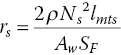
where ρ is the resistivity of the winding material (ohm‐m), l is its length (m) and A is the cross‐sectional area of the conductor (m2). In terms of the transformer parameters, we assume that half of the window area is allocated to the primary winding and half to the secondary. We can therefore express the winding resistance as:

where rp is the resistance of the primary winding, Np is the number of primary turns, lmtp is the mean turn length of the primary winding, Aw is the window area ![]() and SF is the space factor = the fraction of the window area occupied by copper.
and SF is the space factor = the fraction of the window area occupied by copper.
It is interesting to note that where the volume available for the primary winding is constrained, the primary resistance is proportional to the square of the primary turns Np. Similarly, the secondary resistance can be written:
where Ns is the number of secondary turns and lmts is the mean turn length of the secondary winding (m).
Finally, the resistive component of the short‐circuit impedance, referred to the secondary is given by:

Equations (7.3) and (7.4) suggest that the X/R ratio is independent of the number of turns on either winding.
7.1.1 Magnetic Circuit Architecture
A three‐phase transformer can be constructed from three single‐phase devices, each with a separate magnetic circuit, and early in the twentieth century this method was often used, each transformer being enclosed in its own tank. A more common approach, however, is to fabricate a single magnetic circuit capable of supporting the flux generated by each phase, thereby permitting the transformer to be housed in a single tank.
The construction of a three‐phase, single magnetic circuit transformer can be achieved by merging three single‐phase cores as suggested in Figure 7.3. When excited by a set of positive (or negative) sequence voltages, the common leg of the resulting transformer core effectively carries no flux, as the flux components from each of the three phases add to zero at every instant in time.

Figure 7.3 Flux cancellation in the centre limb.
Therefore when constructing a three‐phase transformer, it is not always necessary to provide a common limb. In the very early part of the twentieth century some transformers were built in exactly this manner, as shown in Figure 7.4a, but it was soon realised that the magnetic circuit could also be built in one plane, with only a slight loss of magnetic symmetry, as shown in Figure 7.4b.

Figure 7.4 (a) Very early core form distribution transformer (5 kV:120 V, 150 kVA – the third phase lies behind the other two) (b) A partially dissected core form transformer.
The magnetic circuit arrangement shown in Figure 7.4 is known as a core form construction, in which one limb (or leg) is provided for each phase, i.e. a three‐limb core. These magnetic circuits are quite capable of supporting positive (or negative) sequence flux, since the three flux components sum to zero in the upper and lower parts of the magnetic circuit (known as yokes).
On the other hand, if a zero‐sequence current were to flow through each phase winding, the core type magnetic circuit would present high magnetising reluctance, since no metallic return path exists for zero‐sequence flux. We might therefore expect that the zero‐sequence flux would be very small in such cases, as the return path must be set up in the air surrounding the core. As a result, the back EMF induced in each winding, per amp of zero‐sequence current, will be small, as will the zero‐sequence impedance (Z0) of the transformer.
A second magnetic circuit arrangement also used in the manufacture of three‐phase transformers, is depicted in Figure 7.5. This arrangement, known as a shell form magnetic circuit, has one limb for each phase plus two others which carry no windings, i.e. it is a five‐limb core.

Figure 7.5 (Three‐limb core form on the left and five‐limb shell form on the right). Three‐phase core and shell form magnetic circuits.
In the case of the shell form construction, the magnetic circuit for each phase is effectively separate, since a complete flux path exists independent of the other two phases. The five‐limb shell architecture can thus be compared to the case where three separate single‐phase transformers are used to collectively fabricate a three‐phase device, each magnetic circuit being entirely separate from the others. The same is not true, however, of the more common core form construction shown on the left of Figure 7.5, where the three magnetic circuits clearly have a degree of flux linkage.
Consider the operation of a shell form transformer with a zero‐sequence current flowing in its windings. Because each phase effectively has its own magnetic circuit, a relatively large zero‐sequence flux can exist in each limb (as would be the case in a single‐phase transformer), thereby generating a substantial back EMF in each winding. As a result, the zero‐sequence impedance presented by a shell form transformer can be large.
7.2 Transformer Zero‐Sequence Impedance
The positive and negative sequence impedances of three‐phase transformers are identical since, as mentioned earlier, reversing the phase sequence makes no difference to the operation of a transformer. The zero‐sequence impedance on the other hand, depends upon both the choice of core architecture and the winding arrangement used.
Shell form cores have the ability to support a zero‐sequence flux, provided the winding arrangement employed can pass the necessary zero‐sequence current to generate one. In cases where a zero‐sequence flux can be generated, a large zero‐sequence impedance exists, equal to the magnetising impedance of the core concerned. However, if the current becomes large enough to saturate the core, Z0 will fall to a quite a low value.
In contrast core form transformers cannot readily support zero‐sequence flux and therefore generally exhibit low zero‐sequence impedances where the winding arrangement permits it. However, the presence of nearby metallic components such as a tank wall or clamping structures can provide a partial return flux path, enabling a small zero‐sequence flux to become established within the core, leading to an increase in Z0.
The ability of a winding to carry any zero‐sequence current depends on the connection arrangement used. Delta connected windings cannot deliver zero‐sequence currents since they provide no return path and hence Z0 will be infinite. (A zero‐sequence current can however circulate within a delta winding, provided a zero‐sequence flux is established within the core limbs to excite one.) The zero‐sequence performance of star connected windings depends on whether the neutral is grounded. A grounded neutral terminal provides the necessary return path for zero‐sequence currents, enabling a zero‐sequence flux to be established within the core. A floating neutral on the other hand, precludes the passage of zero‐sequence currents in a similar fashion to a delta connection, yielding an infinite zero‐sequence impedance.
Transformers with at least one grounded star winding will provide a local zero‐sequence impedance to ground, the magnitude of which depends on the core architecture. Whether a transformer can pass zero‐sequence currents from one winding to the other depends on both winding arrangements. A star‐star wound transformer for example with both neutrals grounded can pass zero‐sequence currents from one winding to the other. Such a transformer presents a low impedance to through currents, since flux cancellation between windings removes most of the zero‐sequence flux. In this case Z0 will generally equal Z1 regardless of the core architecture.
Consider a Yy connected shell form transformer with an earthed HV star point, and a floating LV star point. A high Z0 value will be presented to HV zero‐sequence currents and an infinite one on the LV side. The same transformer when fitted with a closed tertiary delta winding, will exhibit a much lower HV Z0 value. This is due to the flux cancellation between the zero‐sequence current flowing in the HV windings and that circulating within the delta. The zero‐sequence impedance to ground will therefore be equal to the sum of the leakage impedances of both these windings.
A set of zigzag connected windings with a grounded star point, as shown in Figure 7.6, is often employed in the construction of earthing transformers. This is because the series connection of phase windings causes a zero‐sequence flux cancellation in each limb, yielding a particularly low Z0 value, equal to the leakage reactance between the two. On the other hand such a cancellation does not occur for positive or negative sequence flux, and therefore a much higher magnetising impedance is presented to these currents. Thus a grounded zigzag winding will easily support positive and negative sequence potentials, while presenting very little impedance to zero‐sequence currents, which only arise during ground faults. Therefore it is usual to insert a current transformer in the ground connection of an earthing transformer to detect zero‐sequence fault currents.

Figure 7.6 Zigzag connected earthing transformer and phasor representation.
7.3 Transformer Vector Groups
Single‐phase transformers generate secondary voltages that are almost exactly in phase with the potential applied to the primary, and while the same is true of three‐phase devices, an inherent phase shift arises when line voltages on one winding are used to create phase voltages on the other. For example, a 30° phase shift will exist between the primary and secondary phase potentials in a delta‐star (delta‐wye) connected transformer shown in Figure 7.7. The delta connected HV windings are excited by line voltages, but phase voltages are generated in the star connected LV windings.

Figure 7.7 Vector grouping for the Dyn11 connection.
Because of this it is necessary to specify precisely to which vector grouping a given transformer belongs. Vector groups are a simple way of representing both the winding arrangements and the associated phase shift inherent in a transformer. An alphabetic code is used to define the winding arrangement, and a numeric suffix denotes the resulting phase shift.
There are principally three winding arrangements that can be used on either the primary or the secondary winding of a three‐phase transformer: star (wye), delta and zigzag. Accordingly it is necessary to clearly identify the appropriate arrangement used in the vector group code. These connections are identified by Y or y, D or d and Z or z, respectively, depending on whether they are HV or LV windings. The connection used on the high voltage winding is specified by a capital letter which appears first in the vector grouping, while the low voltage winding is identified by a lowercase letter which appears second. In cases where there are more than two windings, this convention is repeated. If the neutral terminal of either winding is brought out of the tank, it is noted accordingly in the vector group, N for HV and n for LV.
The phase shift across the transformer is represented by a numerical suffix to the code. The phase shift of the secondary winding is measured with reference to the corresponding primary voltage. A clock face convention has been adopted where a primary phase voltage is assigned the 12 o’clock position. Secondary phase shifts are represented in multiples of 30°, and the phase shift through a transformer is the angle by which the secondary phase voltage lags the corresponding primary one. This is expressed according to the positions of the hours on the face of the clock.
For example the Dyn11 connection represents an HV winding that is delta connected and an LV winding that is star connected, as shown in Figure 7.7. The phase shift arises because although each pair of associated windings is wound on the same leg, the voltage across the LV winding represents a phase voltage while that across the primary is a line voltage. Figure 7.7 shows that if the C‐N primary voltage is chosen as the reference at the 12 o’clock position, then the c‐n secondary voltage lies in the 11 o’clock position. In other words, it lags behind the reference phasor by 11 × 30° or 330°.
Figure 7.7 deserves further comment; clearly it is based on a phasor diagram, but it also shows the terminals of each winding, A, B and C for the HV windings, and a, b, c and n for the LV windings. Notice that voltages VAB and Van lie in phase with each other; this is because the associated windings are wound on the same core leg. Therefore windings CA and cn are also on the same core leg, as are windings BC and bn.
The vector group depends upon which winding is the HV and which is the LV. For example, the Dy11 connection shown in Figure 7.8 will become Yd1 when the HV and LV windings are interchanged. The phase identifiers between such pairs of groups add to either 12 or zero. Vector connections are known as true when both windings on the same leg are associated with the same phase. Untrue groups arise when windings are transposed from one phase to another.

Figure 7.8 Zigzag vector group, Dz6.
The zigzag connection uses series connected windings from two core legs, as depicted in Figure 7.8, to support each phase voltage. This introduces an inherent phase shift between primary and secondary, which can be adjusted according to the connection used and the number of turns on each winding. The zigzag connection is frequently used to introduce small phase shifts between transformers.
Figure 7.9 shows some common vector groupings for two winding transformers.

Figure 7.9 Some common vector groupings.
(IEC 60076‐1 ed.3.0 Copyright © 2011 IEC Geneva, Switzerland. www.iec.ch).
7.4 Transformer Voltage Regulation
Because of its short‐circuit impedance a transformer’s secondary terminal voltage does not remain constant as load is applied. Moreover, the output voltage depends upon the power factor of the load as well as its magnitude in VA. Transformer voltage regulation is defined by Equation (7.5).

where |E2| is the magnitude of the open circuit output voltage and |V2| is this voltage under loaded conditions (see Figure 8.6). The regulation is equal to the per‐unit drop in output voltage with respect to the loaded output voltage, and is expressed in per cent. It is a scalar quantity.
The output voltage differs from the secondary winding voltage by the drop across the short‐circuit impedance. If we consider the primary series impedance elements r1 and x1 reflected to the secondary side, we will see in Chapter 8 that:

where R is the resistive component of the load impedance and X is its reactive component. In this analysis the load consists of elements R and X connected in parallel, and r and x are the real and reactive components of the short‐circuit impedance, i.e. ![]() and
and ![]() respectively, referred to the secondary. Finally, it is assumed that
respectively, referred to the secondary. Finally, it is assumed that ![]() and
and ![]() . It is useful to express all these parameters as per‐unit quantities. Equations (7.5) and (7.6) can be combined to yield:
. It is useful to express all these parameters as per‐unit quantities. Equations (7.5) and (7.6) can be combined to yield:

Further, since in many transformers the X/R is ratio lies between 10 and 50, the resistive term can sometimes be ignored, leading to the approximate result:

Equation (7.7) is significant, since it predicts approximately how the voltage regulation varies as the load changes. For small loads, both R and X will be large, and the regulation will be low, i.e. the output voltage will scarcely change. However, as the load increases, both R and X will decrease, leading to an increase in both the resistive and reactive voltage drops, and hence a fall in the output voltage. This will also be accompanied by a slight phase shift across the transformer’s impedance.
Figure 7.10 shows how the regulation varies as a function of power factor for a constant VA load. In this example r = 0.01 pu and x = 0.06 pu, and the load impedance has been set at 1 pu, independent of the power factor, i.e. ![]() . The load power factor is equal to cos(arctan (R/X)).
. The load power factor is equal to cos(arctan (R/X)).

Figure 7.10 Transformer regulation as a function of power factor, for a 1 pu load.
Figure 7.10 includes both positive and negative values for X, corresponding to inductive and capacitive loads, or lagging and leading power factors respectively. Although for phase angles less than ±90° the power factor is always positive, in Figure 7.10 lagging power factors are defined as positive while leading power factors are negative. (This terminology is frequently used in energy metering applications to clearly distinguish between lagging and leading loads.)
The figure shows that at unity PF the regulation is small and positive (0.01 pu). This is simply due to the r/R term. As the load becomes inductive, the regulation increases rapidly and the output voltage falls. This is due to the fact that x > r and therefore as the inductive component increases so does the regulation. It flattens as the PF decreases further, peaking when the voltage dropped across r + jx lies in phase with the output voltage V2. This occurs when ![]() . As the power factor continues to decrease, the regulation improves slightly.
. As the power factor continues to decrease, the regulation improves slightly.
The regulation curve becomes particularly interesting when the power factor is leading, i.e. as the load becomes capacitive. In these circumstances the x/X term is negative and the regulation decreases as a result and the terminal voltage will exceed that in the winding. When the load power factor reaches ![]() , the reactive term will cancel the resistive term and the regulation will equal zero. This means that the magnitude of the winding EMF and the transformer terminal voltage will then be equal.
, the reactive term will cancel the resistive term and the regulation will equal zero. This means that the magnitude of the winding EMF and the transformer terminal voltage will then be equal.
As the power factor becomes progressively more capacitive, the reactive term begins to dominate and the regulation becomes negative, and therefore the output voltage rises beyond the secondary winding potential. In this case it reaches a minimum of −0.06 pu when the load is entirely capacitive; the regulation then being equal to − x/X. This behaviour is typical of the situation where a voltage support capacitor connected to an inductive source generates a small voltage rise.
7.4.1 Voltage Regulation in Yy Transformers without Flux Linkage
One disadvantage of Yy transformers where there is no flux linkage between phases lies in their ability to support unbalanced loads. Consider the case of a three‐phase shell form transformer comprising a five‐limb magnetic circuit. Because of its construction this type of transformer provides a low reluctance path for the production of zero‐sequence flux and therefore it presents a high zero‐sequence impedance. This presents two problems: the first as mentioned above is the inability to supply unbalanced loads, while the second relates to the low value of earth fault or zero‐sequence currents that will flow in the transformer under fault conditions. This restriction may make the detection of earth faults difficult.
The voltage regulation of an asymmetrically loaded Yy transformer can be most easily understood in the case where a load is applied to one secondary phase only and where no primary neutral connection exists (which is frequently the case). In such a situation the primary current required by the loaded phase must be supplied via the other two, but since these are only carrying magnetising current, they appear as large inductive impedances. Accordingly the loaded phase voltage falls while the other two rise, generally asymmetrically.
This situation is illustrated in the following example. A 6 kVA three‐phase Yy transformer consists of three 2 kVA single‐phase units, and when loaded asymmetrically the loaded phase voltage falls while the others rise, as shown by the tabulated results below.
Table 7.1 shows that for a small asymmetrical load (0.03 pu, resistive) a Yy transformer exhibits a substantial change in phase voltages. This has been caused by a shift in the star point of the secondary winding. Such a situation occurs because of the generation of a zero‐sequence flux within each leg and thus a zero‐sequence voltage within each winding. The phasor diagram corresponding to this example appears in Figure 7.11. The zero‐sequence voltage (V0) can be shown to be equal to the shift in the star point voltage (i.e. VNN′).
Table 7.1 Measured phase voltages on an asymmetrically loaded Yy transformer without flux linkage.
| Phase | No load voltage (pu) | Phase to neutral load (pu) | Loaded phase voltage (pu) |
| A | 1.0 | 0 | 1.56 |
| B | 1.0 | 0 | 1.15 |
| C | 1.0 | 0.03 | 0.73 |

Figure 7.11 Presence of a zero‐sequence voltage (V0), shifts the star point from N to N′.
The situation can be remedied by the provision of a set of delta connected windings that generate a zero‐sequence flux sufficient to cancel nearly all of the offending voltageV0.
Table 7.2 shows the effect of including a closed delta winding on the transformer used in the previous example. Here we observe very small changes in phase voltage on the unloaded phases, as a result of a substantial load increase on the C phase. Clearly the delta winding has cancelled most of the zero‐sequence voltage and has restored the regulation. For these reasons delta connected tertiary windings are usually fitted to Yy shell form transformers.
Table 7.2 Measured phase voltages on a Yy transformer without flux linkage, incorporating a closed delta winding.
| Phase | No load voltage (pu) | Phase to neutral load (pu) | Loaded phase voltage (pu) |
| A | 1.0 | 0 | 1.01 |
| B | 1.0 | 0 | 1.00 |
| C | 1.0 | 0.32 | 0.97 |
7.4.2 Voltage Regulation in Yy Transformers with Flux Linkage
How would this situation have changed had a core form transformer been used instead, i.e. one where a flux linkage exists between phases? In this case, the flux created by the secondary current on the loaded phase must split and return via the other two legs. By so doing, each of those phases would draw an equivalent primary balance current which collectively would be exactly sufficient to match that from the loaded phase. As a result, the star point voltage will not see a shift and therefore there will be no zero‐sequence voltage developed. The data in Table 7.3 illustrates such an instance for a similarly sized core form transformer, under a heavy asymmetrical load.
Table 7.3 Measured phase voltages on an asymmetrically loaded core type Yy transformer.
| Phase | No load voltage (pu) | Phase to neutral load (pu) | Loaded phase voltage (pu) |
| A | 1.0 | 0 | 0.93 |
| B | 1.0 | 0 | 1.05 |
| C | 1.0 | 0.46 | 0.94 |
Finally, Table 7.4 shows the effect of including a delta tertiary winding on this transformer. From the foregoing discussion we might not expect a closed delta winding to provide much of a phase voltage improvement on a transformer with good flux linkage between phases, and from Table 7.4 this would appear to be the case; however, there is a slight improvement. This is likely to be due to the fact that even when a flux linkage exists between phases, it is still possible for a small zero‐sequence flux to exist in the core. A closed delta winding may therefore result in a small improvement in regulation and a reduction in the unbalance between phase voltages.
Table 7.4 Measured phase voltages on a core form Yy transformer incorporating a closed delta winding.
| Phase | No load voltage (pu) | Phase to neutral load (pu) | Loaded phase voltage (pu) |
| A | 1.0 | 0 | 1.00 |
| B | 1.0 | 0 | 1.00 |
| C | 1.0 | 0.46 | 0.94 |
7.5 Magnetising Current Harmonics
Figure 7.12 shows the magnetising current and flux waveforms for a single‐phase transformer to which a sinusoidal voltage has been applied. Since the flux density is proportional to the integral of this voltage, then it too must have a sinusoidal waveform. However, in order to generate this, the magnetising current must take on high peak values, as demanded by the B–H loop. As a result the magnetising current is rich in low order odd harmonics, in particular the third, which assists the core in achieving its peak flux density.

Figure 7.12 Magnetising current, flux density and voltage waveforms in a single‐phase transformer.
As we will see in Chapter 13, the harmonics inherent in a balanced set of non‐sinusoidal currents tend themselves to be balanced. This means, for example, that the 5th harmonic component of such a set of currents will exist as an individually balanced system, where each phase current has the same magnitude and is separated from its neighbours by 120°. Harmonic currents also have similar properties to those of the fundamental; in particular, they can be shown to have positive, negative or zero‐sequence characteristics. Table 7.5 shows the sequence classification of some low order odd harmonics. Even harmonics tend to cancel in symmetrical current waveforms and, except during start‐up, these generally do not appear in a transformer’s magnetising current.
Table 7.5 Characteristics of different harmonics.
| Harmonic number | Characteristics |
| 3rd | Zero sequence |
| 5th | Negative sequence |
| 7th | Positive sequence |
| 9th | Zero sequence |
| 11th | Negative sequence |
Harmonic currents that are a multiple of three times the fundamental frequency are zero‐sequence harmonics. They are co‐phasal and are often referred to as triplen harmonics, and as a result they cannot flow towards an isolated star point, as can positive or negative sequence currents. Similarly, they cannot flow towards a set of delta connected windings, and therefore transformers that present a high zero‐sequence impedance also exclude the triplen harmonic component from their magnetising current. This can have an unexpected effect on the resulting winding voltages.
7.5.1 Magnetising Current in Star Connected Shell Form Transformers
Consider the case of a three‐phase shell form transformer (or three single‐phase transformers) with star connected primary windings and no neutral connection. In this case there is no path for triplen currents to flow, since the star point is isolated from ground. The magnetising current therefore consists of a component at the fundamental as well as the low order odd non‐triplen harmonics (i.e. 5th, 7th, 11th etc.). As a result, the flux waveform is flat topped and passes through zero at a slightly faster rate than in the case of a sinusoidal flux waveform, as shown in Figure 7.13.

Figure 7.13 Magnetising waveforms for a shell form star connected transformer.
Each phase voltage contains a significant third harmonic (triplen) voltage in addition to one at the fundamental frequency, as illustrated in Figure 7.14. This causes an ‘oscillation’ as the waveform passes through zero, as well as a slightly peaky maximum.

Figure 7.14 Presence of a third harmonic voltage in each phase winding causes the star point to oscillate at the third harmonic.
This zero‐sequence triplen voltage creates an oscillation in the star point (S) with respect to the supply neutral, as shown in Figure 7.14. The triplen potential cancels in the line voltages which, as expected, remain sinusoidal.
Effect of a Tertiary Delta Connected Winding
If a closed delta winding is incorporated into such a transformer (a tertiary delta), the situation alters significantly. Zero‐sequence triplen voltages induced into each of the delta windings cause a third harmonic current to circulate within the delta. The combined effect of these ampere‐turns is to restore the flux waveform in each leg to very near sinusoidal and, as a result, the phase voltages become sinusoidal, as shown in Figure 7.15, and the star point voltage oscillation ceases.

Figure 7.15 Magnetising waveforms in shell type transformer incorporating a delta connected winding.
The flux restoration process that leads to almost sinusoidal phase voltages can be understood from Figure 7.15, which shows the magnetising current flowing in the star connected primary winding, as well as the triplen current flowing in the delta. If these ampere‐turns are added, the resulting waveform resembles the magnetising current shown in Figure 7.12 for a single‐phase transformer, and thus a sinusoidal flux waveform is generated. This beneficial effect represents another reason why a tertiary delta winding is usually included in star connected shell form transformers.
7.5.2 Magnetising Current in Star Connected Core Form Transformers
Since core form transformers cannot support a zero‐sequence flux (either at the fundamental or at a triplen harmonic) neither can they support the oscillating neutral potential described above. The flux waveform will therefore be sinusoidal, generated by a magnetising current rich in odd harmonics. Whether triplen harmonics are present depends on the neutral termination. A grounded neutral will provide a path for triplen currents to flow, and the magnetising current will look similar to that shown in Figure 7.12. An ungrounded neutral will block this path and the magnetising current will contain higher levels of the 5th and 7th, but in both cases the flux waveform will remain nearly sinusoidal, and the neutral terminal will therefore lie close to ground potential. As a result, the phase voltages will generally be close to sinusoidal.
Figure 7.16 shows the magnetising characteristics of a core form transformer with an isolated neutral. The magnetising current is rich in odd non‐triplen harmonics, and the peak flux density is achieved through the presence of elevated levels of the 5th and 7th. The resulting phase voltage is very nearly sinusoidal.

Figure 7.16 Magnetising characteristics of a core type transformer with an isolated neutral. (Note that the magnetising current contains significant levels of the 5th and very little 3rd harmonic).
7.5.3 Magnetising Current in a Delta Connected Winding
When the excited winding is delta connected, a sinusoidal flux must be induced within the core capable of supporting the applied line voltage. Since third harmonic currents cannot flow from the supply towards a delta winding, the magnetising current contains components at both the fundamental plus odd non‐triplen harmonics. This generates a slightly flat‐topped flux waveform similar to that shown in Figure 7.13, which induces a small third harmonic potential in each winding. In a similar fashion to the tertiary delta winding discussed above, this voltage sets up a small third harmonic circulating current, which restores the flux waveform to a sinusoidal shape as shown in Figure 7.17. The small third harmonic voltage is dropped entirely across the winding impedance and therefore it does not appear in the line voltage.

Figure 7.17 Magnetising characteristics for a delta connected winding.
7.5.4 Transformer Inrush Current
The magnetising current waveforms shown in the previous illustrations correspond to steady‐state transformer operation, by which time any start‐up transients will have died away. At all times, the applied voltages must be matched by the potential induced within each winding, and depending on the point on the voltage waveform when the transformer is energised, the magnetising current required to ensure this may become very large and asymmetrical. This phenomenon is known as inrush current, and it can exist in a large transformer for many seconds before finally achieving its steady state, by which time the magnetising current is again small and symmetrical.
Figure 7.17 shows that during each positive half cycle of the voltage waveform, the flux in the core must change from ![]() to
to ![]() , a change of
, a change of ![]() , with a similar situation occurring during a negative half cycle. Therefore if a demagnetised transformer is energised at a voltage zero, during the next half cycle the flux must increase from zero to 2ϕmax. This flux change may be further increased should a residual flux be present in the core prior to switch on.
, with a similar situation occurring during a negative half cycle. Therefore if a demagnetised transformer is energised at a voltage zero, during the next half cycle the flux must increase from zero to 2ϕmax. This flux change may be further increased should a residual flux be present in the core prior to switch on.
Because the initial flux change is uni‐polar, the resulting magnetising current will become very large and asymmetrical and may temporarily exceed the rating of the transformer. A flux swing of this magnitude will usually not be achieved in practice, since a portion of the applied voltage will be absorbed by the source impedance as well as the impedance of the primary winding itself, due to the large current flow. The effect of these losses is to progressively reduce amplitude of both the flux change and the magnetising current, and to restore their symmetry about the time axis. In a large transformer this process can take tens of seconds, during which time the transformer can appear to have an internal fault, since primary current is consumed that is unmatched by a proportional secondary current.
On the other hand, if a transformer is energised at a voltage maximum, the flux waveform increases from zero towards ϕmax before returning to zero 90° later. In this case, the steady state is achieved instantly without the need for a transient inrush current. Unfortunately, it is not possible to simultaneously energise all three phases of a transformer at a voltage maximum, and therefore there will always be some degree of inrush current on energisation.
Figure 7.18 shows the inrush currents for a three‐phase transformer energised when the phase A and B voltages were approximately equal, and the phase C voltage was close to a voltage maximum. The A and B phase magnetising currents are uni‐polar, each containing a decaying DC component. After a period of time all three phases will achieve steady state operation, characterised by small and symmetrical magnetising currents.

Figure 7.18 Measured inrush current waveforms.
7.6 Tap‐changing Techniques
Since system voltages tend to vary with diurnal changes in loading, steps must be taken to maintain them within acceptable limits. This is frequently done by switching shunt capacitors banks into the network as the load increases and also by changing taps on both transmission and distribution transformers. We have seen in Section 7.4.1 that as the load on a transformer increases the transformer regulation generally causes the secondary voltage to decrease. Therefore in order to maintain a constant secondary potential the turns ratio must be increased accordingly. This can be done either by increasing the number of secondary turns slightly or by decreasing the number of primary turns.
Equation 4.13 shows that the voltage‐per‐turn of the primary winding is proportional to the peak flux density ![]() to which the core is excited:
to which the core is excited:
Therefore provided that the ratio of the applied voltage to the number of turns remains constant, the excitation level will not alter. Selecting taps to maintain a constant secondary voltage as the primary potential varies will therefore not change the excitation level of a transformer. This is known as a constant flux voltage variation (CFVV).
It is often necessary, however, to further increase the secondary voltage of a distribution transformer in order to compensate for the regulation losses within the transformer itself, as well as those in the downstream network. To achieve this, the turns ratio must be reduced slightly independent of the applied voltage. This will lead to an increase in the flux density in the core and a proportional increase in the secondary voltage as well. Operation of the tap‐changer in this mode is called variable flux voltage variation (VFVV) and both the voltage‐per‐turn and the inter‐tap potential vary with the tap selected.
Most network transformers are required to maintain one winding voltage within prescribed limits, regardless of the applied load, and therefore their tap‐changer operations will usually include a mix of these categories. This is referred to as combined voltage variation (CbVV), and sufficient headroom must be provided in the transformer’s design to accommodate the additional flux density required if saturation is to be avoided.
Tap changers may be installed on either the HV or the LV winding, but they are usually installed in the HV winding, where the current is lower and the number of turns higher.
7.6.1 Off‐Load Tap Changers
Small pole‐ or pad‐mounted distribution transformers usually have off‐load tap‐changers, sometimes called off‐circuit tap‐changers or de‐energised tap‐changers. These usually have between five and seven tappings included in the HV winding that can be used to adjust the number of HV turns in order to appropriately set the transformer’s LV potential. These tap‐changers are based on a simple selector switch and cannot be adjusted under load, and therefore the transformer must be de‐energised whenever a tap adjustment is made. Figure 7.19 shows three arrangements commonly used to accommodate off‐circuit tap‐changers. The first is a line end arrangement for delta windings, where the tap‐changer is located at a line terminal of each winding. The second is a mid winding arrangement which reduces the voltage that must be accommodated by the tap‐changer to half the phase voltage. The third, places the tap‐changer at the neutral end of a star connected winding, thereby placing the tapping voltages close to zero.

Figure 7.19 Off‐load tap‐change arrangements.
(Adapted and reprinted with permission from IEEE. Copyright IEEE C57.131 (2012). All rights reserved. Permission for further use of this material must be obtained from IEEE. Requests may be sent to: stds‐[email protected]).
7.6.2 On‐Load Tap Changers
Larger transmission and distribution transformers must be capable of tapping under load and therefore are fitted with on‐load tap‐changers or simply load tap‐changers (LTC). These must be able to maintain supply during tap‐changing, while providing an almost indiscernible voltage change. This requirement generally means that a large number of taps must be available. In contrast to an off‐load tap‐changer, a load tap‐changer is quite complex electromechanical device and occupies a substantial portion of a transformer’s volume.
There are two basic types of tap‐changer, both of which operate on a similar principle, as illustrated in Figure 7.20. In order to maintain the flow of load current, it is necessary to draw current from two tappings simultaneously throughout part of the tap‐change. This process obviously cannot involve short‐circuiting the tappings concerned. Therefore an impedance must be provided between them, one that will permit load current to flow from either tap without creating an appreciable load voltage drop and without permitting an excessively large circulating current to flow between taps. These schemes are shown in Figure 7.20, and both include inter‐tap impedances.


Figure 7.20 (a) Resistive tap‐changer (b) Reactive tap‐changer (both shown in the bridging position).
The arrangement shown in Figure 7.20a uses a bridging resistor (or transition resistor) between taps. This type is known as the high speed resistive tap‐changer, and because of the limited capacity of the resistive elements to dissipate heat, the tap‐change is designed to occur in about 50 milliseconds. The second arrangement, shown in Figure 7.20b, is known as a reactive tap‐changer, and uses an autotransformer to support the inter‐tap voltage (also known as a preventive autotransformer). This has the advantage that it can carry load current continuously in the bridging position (shown below), and can thus be used to provide an intermediate voltage between adjacent taps and can therefore reduce the number of taps required on the tapping winding.
7.6.3 High Speed Resistive Tap Changer
The high speed resistive tap‐changer is probably the most widely used type today, largely because of its compact size. Resistors are used to limit the circulating current during the tap‐change process, and since these must be present in the circuit for a very brief period, the operating mechanism is designed to rapidly switch between taps.
In addition to the bridging resistors, there are two types of switch generally associated with this tap‐changer; these are shown in Figure 7.21. The first are the selector switches, used to select the required tapping. Two sets of these are provided, one for the current tap and one for the next tap to be selected. These switches are not opened under load and hence do not suffer arcing damage and are therefore located within the main transformer tank. The second are the diverter switches (also called the arcing switches), designed to carry the arc created when the load circuit is partially interrupted.

Figure 7.21 Tap changer selector and diverter switches.
The diverter switch has four contacts operated in rapid succession, usually by a spring‐powered mechanism, so that the transition resistors are only briefly energised. Because these switches operate under load, they are prone to arcing and create carbon and combustible gasses in the surrounding oil. To avoid contaminating the oil in the main transformer tank, they are located in a separate diverter tank with its own oil reservoir. Contact wear must also be monitored and replacement contacts fitted as required.
Numerous schemes have been derived for switching between taps. We will only consider the flag cycle tap‐change, so called because of the appearance of the phasor diagram corresponding to this tap‐change process. This cycle is characterised by the fact that load current is diverted to one transition resistor before the resistive bridge between the taps is completed and circulating current begins to flow.
Figure 7.22 illustrates the flag sequence for a tap‐change between taps 1 and 2. Initially tap position 1 is selected and current flows from this tap to the load, via selector switch S1 and the left‐hand diverter switch, Figure 7.22A. The tap‐change commences when the diverter switch rotates to include resistor R1. The load current path initially remains unchanged. In Figure 7.22C the diverter switch has moved, and now the entire load current briefly flows via R1. By Figure 7.22D both R1 and R2 are available to carry the load and current is shared between taps 1 and 2, half flowing from each. At this time, the terminal voltage lies midway between taps 1 and 2, less the IR drop across the resistors. In Figure 7.22E, R1 has been switched out of circuit, and the entire load current now flows via R2, from selector switch S2. As the diverter switch rotates further (Figure 7.22F), this current is switched out of R2, and by Figure 7.22G all the current flows directly from S2 and the tap‐change is complete.

Figure 7.22 Resistive tap‐change flag cycle operating sequence.
At this point, selector switch S1 may move to tap 3 should a further increase in winding potential be required. The complete operation occurs in about 50–100 ms, thus the energy that must be dissipated by the resistors is relatively small. The diverter switch has only two stable states, corresponding to Figures 7.22A and 7.22G and once triggered the tap‐change cycle proceeds rapidly from one to the other.
Flag Cycle Phasor Diagram
The phasor diagram corresponding to this sequence appears in Figure 7.23. We choose the winding voltage as the reference phasor and identify the present tap voltage V1 and the subsequent tap voltage V2. An inductive load current IL is assumed to be flowing from the winding and a resistive circulating current IC will flow between the taps when bridged.

Figure 7.23 Phasor diagram corresponding to the flag cycle tap‐change sequence.
Beginning again at Figure 7.22A, the load voltage is equal to V1 and load current flows via selector switch S1. In Figure 7.22C load current is supplied by the left hand transition resistor; its voltage advances in phase and falls slightly in magnitude to ![]() , point C in Figure 7.23. By Figure 7.22D bridging is complete, and IL/2 flows in each transition resistor and a circulating current IC flows between the taps. The load voltage in Figure 7.22D becomes
, point C in Figure 7.23. By Figure 7.22D bridging is complete, and IL/2 flows in each transition resistor and a circulating current IC flows between the taps. The load voltage in Figure 7.22D becomes ![]() (point D in Figure 7.23), rising to
(point D in Figure 7.23), rising to ![]() by E. Finally at F and G the load current is entirely supplied from tap 2 and its voltage is V2. The load voltage therefore progresses from V1 to V2 via points C, D and E on the phasor diagram in Figure 7.23.
by E. Finally at F and G the load current is entirely supplied from tap 2 and its voltage is V2. The load voltage therefore progresses from V1 to V2 via points C, D and E on the phasor diagram in Figure 7.23.
When oriented vertically, Figure 7.23 resembles a flag and it is from this that the flag cycle sequence gets its name. There are numerous other tap‐change schemes described in the IEEE standard C57.131 ‘IEEE Standard Requirements for Tap‐changers’, each also named after the appearance of its phasor diagram.
7.6.4 Reactive Tap‐Changer
A similar tap selection scheme can be used with the reactive tap‐changer shown in Figure 7.20b, but this design also lends itself to a slightly different mode of operation. Because the autotransformer can be designed to continuously carry full load current, it can be used to generate an intermediate voltage between two adjacent taps. In this configuration half the load current flows through each winding, thereby generating opposing fluxes in the core. This cancels most of the inductive impedance associated with the device, at the expense of a magnetising current, circulating between the selected taps. Using the autotransformer to generate intermediate voltages enables the number of taps to be reduced. This represents a significant saving in the size of the main transformer, since tapping leads tend to increase the size of both the windings and the core.
Reactive tap‐changers are often purchased as an accessory by the transformer manufacturer and also contain the selector and diverter switches described above. Occasionally these switches are combined into one arcing switch which is located in the diverter tank. Since the autotransformer can continuously carry load current so there is no requirement for the diverter switches to operate as rapidly as in the case of the resistive tap‐changer. We will discuss an example of a reactive tap‐changer later in this chapter when we consider the operation of step regulators in Section 7.9.
7.6.5 Vacuum Interrupter Tap Changers
Since the early 1990s, vacuum interrupter technology of the kind used in vacuum circuit breakers has progressively found application in tap‐changers in place of oil‐insulated diverter switches. Vacuum interrupters give very good service and have obviated the need for tap‐changer maintenance altogether in some transformers. In high tapping duty applications such as rectifier, phase shifting and arc furnace transformers, the maintenance interval can often be extended to between five and seven years.
Vacuum interrupters are hermetically sealed canisters in which the current is rapidly broken in a vacuum, and therefore the arcing products created are separated from the surrounding media. They offer a low contact resistance throughout the life of the interrupter, which can exceed 500,000 operations, and do not create the arcing by‐products inherent in oil‐insulated switches. Many manufacturers offer retro‐fittable vacuum based diverter assemblies that can be easily installed in their existing oil based tap‐changers. Vacuum interrupters are also quite capable of operating in free air when required, and are also now finding application in resin cast and small distribution transformers.
Figure 7.24 shows the tapping sequence for a reactive vacuum tap‐changer, which in addition to one vacuum interrupter, also requires two bypass switches in each phase.

Figure 7.24 Tapping sequence vacuum interrupter based diverter switch.
(Adapted and reprinted with permission from IEEE. Copyright IEEE C57.131 (2012) All rights reserved. Permission for further use of this material must be obtained from IEEE. Requests may be sent to: stds‐[email protected]).
7.6.6 Typical Winding Arrangements
There are many different winding arrangements used in tap‐changer circuits, some of which are shown in Figure 7.25. We will analyse the single reversing changeover configuration frequently used in the phase windings of star connected transformers.

Figure 7.25 Common tap winding connections.
A tapping winding is generally wound independent of the phase winding with which it is associated. This permits it to be located at either the line end, the centre or the neutral end of this winding. Of these, the neutral end option minimises the insulation requirements of the tap‐changer, making it particularly attractive in star connected transformers. This particular arrangement is shown in more detail in Figure 7.26, where three windings are provided, all of which are on the same core leg: the main phase winding, across which most of the applied voltage is dropped, the tapping winding, in this case having eight taps, and an auxiliary or tickler winding, the purpose of which will become apparent shortly. A reversing switch is provided, enabling the phase of the tapping winding to be reversed with respect to that of the main winding.

Figure 7.26 Typical tapping winding configuration.
Consider initially the situation when tap 0 is selected. This is the neutral tap, since the tapping winding is not in circuit, thus the phase voltage is applied across the main winding only. If this tap also corresponds to the nominal primary and secondary voltage ratings of the transformer it is also referred to as the principal tap.
Since the reversing switch resides in the main tank, the tap‐change mechanism will only permit it to change state when tap 0 is selected, thus avoiding arc damage and oil contamination. If this switch is initially in position 2, then selecting tap 1 will introduce a small segment of the tapping winding in series with the main winding. However, because of the position of the reversing switch, the voltage across the tapping winding opposes that in the main winding. Since the applied phase voltage is fixed, this now must be supported by effectively fewer turns than previously was the case. Accordingly the transformer’s turns ratio (Ns/Np) has increased slightly, and with it the secondary voltage. Tap 2 will see this effect enhanced, and thus the secondary voltage will progressively increase until tap 8 is reached, at which point the secondary voltage will have achieved its maximum value.
When the reversing switch is in position 1 the situation changes. Tap 8 now introduces a few additional in‐phase turns in series with the main winding, and thus the effective number of turns available to support the phase voltage increases. Accordingly, this will lead to a decrease in the effective turns ratio and with it a decrease in the secondary voltage. Tapping down through the winding will progressively reduce the secondary voltage until tap 1, by which point the lowest secondary voltage will have been reached. The use of a reversing switch therefore effectively doubles the number of available taps.
The tickler winding provides a further doubling effect. It will be noticed that this winding is included in the circuit on every alternate tap, and since the voltage developed across it is exactly half the inter‐tap potential on the tapping winding, it doubles the effective number of tap positions available. This tap‐changer therefore produces a total of thirty‐three tap positions (including the neutral tap), from a total of only eight leads on the tapping winding!
7.6.7 Typical Tap Changer Hardware Components
As mentioned earlier, the diverter switch contacts require maintenance from time to time, and for this reason these are usually easy to withdraw from the diverter tank. Figure 7.27 shows a diverter switch assembly from a rectifier transformer built in the 1970s. In such applications the tap‐changer operates often, usually under high current, and thus there is a need to frequently maintain the diverter switches and replace their insulating oil. In this case, the diverter assemblies are mounted inside a diverter drum consisting of three identical sections each containing the transition resistors and the diverter switch contacts for one phase. The drive shaft, located at the centre of the drum, is operated by a spring‐powered mechanism that drives all three phases simultaneously.

Figure 7.27 Left: diverter switch drum, Right: transition resistors.
The transition resistors each consist of two series connected wafers, immersed in the diverter switch oil supply to assist in dissipating the heat generated by each tap‐change. The diverter switch contacts terminate on the surface of the drum, in the form of a spring‐loaded contact. These mate with fixed contacts on the inside of the diverter tank, and allow the drum to be withdrawn for maintenance. The diverter switch contacts can be seen in Figure 7.28, where each copper‐tungsten contact can be individually replaced as required.

Figure 7.28 Diverter switch contacts (open) inside the diverter drum.
Many transformer manufacturers purchase tap‐changer mechanisms from third‐party suppliers and design their transformer tanks to accommodate tap‐change assemblies like those shown in Figure 7.29. These can be inserted through a circular opening in the tank lid and are suspended from the circular flange sealing the opening. The diverter switches and transition resistors are contained in a fibre glass drum immediately below the transformer lid, thus facilitating their maintenance.

Figure 7.29 High speed resistive tap‐changers.
(Photo courtesy of Guizhou Changzheng Electric Co, PRC).
The selector switches reside beneath the diverter tank, within the main oil supply, which allows easy connection of the tapping leads, and the reversing switch is mounted beside the selector assembly, as shown in Figure 7.29.
7.7 Parallel Connection of Transformers
It is frequently necessary to operate transformers in parallel, to supply a common load. In such situations it is necessary to ensure that paralleled transformers present secondary voltages that have the same phase relationship and are almost equal. Transformers that are of the same vector group and voltage rating will satisfy this requirement. While this represents the norm, it is also possible for certain other vector groups to operate satisfactorily in parallel. For example, a parallel combination of Yy and Dd transformers would operate satisfactorily (if their turns ratios were set appropriately), as would a Yd and Dy pair.
Two transformers having the same impedance and voltage rating will share a common load equally, provided that they operate at the same tap. Differences in tap setting will give rise to a circulating current flowing between the two secondaries, and a bus voltage that lies in between the two secondary potentials.
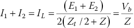
This situation is illustrated in Figure 7.30, where E1 and E2 are the individual winding voltages and Vb is the resulting bus voltage and Z1 and Z2 are the respective transformer impedances. Z is the load impedance and currents I1 and I2 flow in each winding.

Figure 7.30 Parallel transformer equivalent circuit.
The bus voltage Vb can be determined using Millman’s Theorem as:

or

where the admittances Y1, Y2 and Y correspond to the impedances Z1, Z2 and Z respectively.
We also know that  and
and  . Substituting Equation (7.8) into these equations yields:

and

The second term in the above equations is interesting. When ![]() this term becomes zero, and therefore:
this term becomes zero, and therefore:

and

Thus the winding currents are determined by the relative transformer impedances. Multiplying Equations (7.10) and (7.10a) by the bus voltage gives the VA loading seen by each transformer:

Therefore the fractional load carried by one transformer depends on the impedance of the other. It is possible that with dissimilar transformers, the heavier load may ironically be carried by the smaller transformer.
When ![]() , the second term in Equation (7.9) becomes approximately
, the second term in Equation (7.9) becomes approximately  , which can become very large, even for moderate values of
 ![]() , due to the generally small values of the transformer impedances, Z1 and Z2. This highlights the need to ensure that the winding voltages are similar in both magnitude and in phase.
, due to the generally small values of the transformer impedances, Z1 and Z2. This highlights the need to ensure that the winding voltages are similar in both magnitude and in phase.
Consider the case where the paralleled transformers have the same impedance (Zt) but are not operating from the same tap, i.e. ![]() . Ignoring the small effect of the load impedance, the bus voltage in this case will lie roughly midway between E1 and E2. A circulating reactive current will exist between them, of a magnitude sufficient to support this voltage difference. The higher voltage transformer will deliver VArs to the load as well as to its partner. Depending on the VAr flow demanded by the load and the voltage difference, the lower voltage transformer may even consume reactive power. It will certainly deliver less reactive power to the load and will therefore operate at a higher power factor than its partner. (This effect can be used to advantage by deliberately operating dissimilar transformers out of step so as to ensure that they both operate close to the same power factor.) This situation is depicted in Figure 7.31.
. Ignoring the small effect of the load impedance, the bus voltage in this case will lie roughly midway between E1 and E2. A circulating reactive current will exist between them, of a magnitude sufficient to support this voltage difference. The higher voltage transformer will deliver VArs to the load as well as to its partner. Depending on the VAr flow demanded by the load and the voltage difference, the lower voltage transformer may even consume reactive power. It will certainly deliver less reactive power to the load and will therefore operate at a higher power factor than its partner. (This effect can be used to advantage by deliberately operating dissimilar transformers out of step so as to ensure that they both operate close to the same power factor.) This situation is depicted in Figure 7.31.

Figure 7.31 Parallel transformer circulating current.
The currents I1 and I2, defined in Figure 7.31, can be shown each to contain a load current component, ![]() together with the circulating current (IC) flowing between the taps. For small voltage differences, roughly half the active power will be supplied by each transformer, therefore we can write
together with the circulating current (IC) flowing between the taps. For small voltage differences, roughly half the active power will be supplied by each transformer, therefore we can write  and
and  , yielding:

Assuming that ![]() , and:
, and:
Equations (7.12 and 7.12a) suggest that the reactive power flow between the transformers is very sensitive to the tap position, whereas the active power flowing in the load is only slightly influenced by the tap position of either transformer, since changing one tap will only mildly influence the load voltage. Where both the impedances and the tap settings are different the approximation in Equation (7.12) is unreliable and a precise analysis using Equations 7.10 and 7.10a is required.
7.7.1 Tap Change Control Strategies
Having seen a little of how paralleled transformers behave, it is instructive to consider some of the tap control strategies used in practice. The principal function of the voltage regulator is to select transformer taps so as to maintain the bus voltage within acceptable limits. This requires the specification of the voltage set point, together with the bandwidth (also called voltage dead‐band), about the set point, within which no tap‐change will be initiated. This is illustrated in Figure 7.32, where Vs is the set‐point voltage, VBus is the bus voltage and BW is the voltage bandwidth. A time delay TD is applied before a tap‐change is initiated, so as to prevent instantaneous tap‐changing in response to short‐term voltage excursions.

Figure 7.32 Voltage set‐point and bandwidth.
(Adapted with the kind permission of the Beckwith Electric Co).
Figure 7.32 shows the case where the bus voltage falls below the lower bandwidth limit. After the delay time TD has expired, the tap‐change is initiated, restoring the voltage to within the acceptable range. In the case of a master‐slave control strategy the master controller initiates the tap‐change on the master transformer and the others are then commanded to follow. In this way, all transformers remain on the same tap, i.e. they remain in step.
If each transformer had an independent controller, the first to initiate the tap‐change may well restore the bus voltage to within the desired dead‐band. This would result in the other transformers remaining in their original tap positions, with an undesirable circulating current now flowing between them. Subsequent voltage disturbances would again see the fastest transformer make a corrective tap‐change, thus driving the others further out of step. Operating similar transformers from different tappings will result in considerable reactive flows between them causing additional I2R losses. The master‐slave control strategy is generally implemented when transformers must be run in parallel.
Power Factor Paralleling Method
The ability to interchange VArs between paralleled transformers permits several other methods to be used for choosing the optimal tap positions of paralleled transformers. One such method is to choose tap settings that will ensure that paralleled transformers operate at about the same power factor while maintaining the bus voltage within limits. This requires the measurement of the current phase angle of each transformer; the controller blocks tap‐changes that would drive these angles further apart, while maintaining the desired bus voltage. This ensures that both transformers operate at similar power factors, thus preventing asymmetrical transformer loading. It should be noted that this control strategy is rarely implemented in industrial power systems.
Circulating Current Method
The circulating current approach aims to minimise the magnitude of any circulating current flowing between transformers. To achieve this, equipment is required that will isolate the circulating current from the load current. With this information the controllers can bias the tap‐change on the high tap transformer so as to reduce its voltage, while doing the opposite for the low tap device. In this way the circulating current is minimised while still maintaining the desired bus voltage.
VAr Balancing Method
This approach operates so as to equalise the VAr contribution from each transformer. In the case where transformers of different ratings are paralleled, the CT ratios should be appropriately chosen so as to reflect these ratings. Thus the sharing can be appropriately apportioned between transformers.
7.8 Transformer Nameplate
The nameplate contains an essential record of a transformer’s voltage, current and VA ratings, its impedance, how its windings are configured, what tappings are available as well as data on accessories such as the cooling equipment and any associated current transformers. As such, it is second in importance only to the factory test report, and therefore it should always remain attached to the transformer. An example of a typical nameplate appears in Figure 7.33, in this case for a 110 kV:33 kV, 60 MVA, YyNn0 distribution transformer. There is no standard layout used by all manufacturers, but all nameplates generally include the following items:

Figure 7.33 Example of a transformer nameplate.
Transformer ratings: Because of their importance, these usually appear somewhere near the top of the nameplate. In this case, the voltage ratings appear in the top right‐hand table, the power ratings are in the column opposite, while the current ratings appear in the tapping chart. It is not uncommon for a transformer of this size to have two power ratings (in this case 42 MVA and 60 MVA) depending on whether fan forced cooling is applied to the radiators. This is indicated as either ONAN (oil natural air natural) or ONAF (oil natural air forced). (Had pumps been provided to circulate oil through the radiators, the latter abbreviation would have read OFAF.)
The upper table also includes information on the withstand capability of the winding insulation, and is characterised by two parameters. The first is the basic insulation level (BIL) or the standard lightning impulse withstand voltage that the transformer is capable of supporting (550 kV in this example). This is the peak value of a unidirectional surge voltage applied between the transformer terminals and ground, having a rise time of the order of 1.2 µs and a time to half‐value of 50 µs. The second is the RMS short duration power frequency withstand voltage (230 kV). Collectively these parameters define the insulation level of the transformer.
Transformer impedances: The positive (negative) and zero‐sequence impedances appear in the second table on the right‐hand side, for taps 1, 7 and 23. The positive sequence impedance associated with each tap position also appears in the tapping table. The impedance varies slightly with each tap, roughly as the square of the effective number of turns on the HV winding, though not necessarily monotonically. In this case, the impedance is relatively high, having been chosen to set the LV fault current at a level suitable for the downstream switchgear. The zero‐sequence impedances are of similar values, indicating that for this core form transformer sufficient leakage flux is established, probably via the tank walls, to permit a zero‐sequence voltage to be generated in each phase as the result of zero‐sequence current flowing in the windings.
Winding configuration and vector grouping: The winding configuration and vector group are shown in the lower right‐hand corner of this nameplate. The HV terminals are always identified by capital letters and the LV by lowercase letters. Windings identified by the same letter are wound on the same limb, therefore the main HV winding A15‐A14, the tapping winding A13‐A1 and the LV winding a2‐a1 are all concentric on the ‘A’ phase limb. The LV winding generally lies closest to the core, and the tapping winding is usually the outermost. The star connected HV winding has the on‐load tap‐changer located at its neutral end where the insulation requirements are less severe.
The HV winding has a current transformer on the ‘B’ phase; this is used to excite the winding temperature indicator with a current proportional to the instantaneous load on the transformer. This information, coupled with the top oil temperature (usually shown on a separate indicator), is used to synthesise a temperature representative of the hotter parts of the windings. The star connected LV windings are fitted with protection class current transformers, located between the neutral terminal and ground, external to the tank.
Temperature limitations: The nameplate also indicates the permitted maximum rise above ambient (40 °C) for the top oil and winding temperatures (60/65 °C respectively), as well as the maximum temperature permitted for the hottest part of the winding (120 °C). These temperatures are determined by the class of insulation used to insulate the windings. The maximum average winding temperature for this transformer would therefore be ![]() , leaving a 15 °C margin for the ‘hot spot’ temperature.
, leaving a 15 °C margin for the ‘hot spot’ temperature.
Tappings: The tapping chart shows the connections required on the HV winding for each of the 23 tap positions. The stated HV voltage on each tap is the no load voltage required to produce the rated voltage (33 kV) at the secondary terminals. On its principal tap, this transformer has current ratings of 220.4 and 314.9 A corresponding to each of its MVA ratings. The associated current ratings vary with the applied HV voltage, in such a way that the overall MVA rating of the transformer remains constant.
Transformer plan view: A plan view of the transformer is always included on the nameplate, showing the HV and LV terminal locations, as well as the location of the radiators and the tap‐changer. Above the radiators is mounted the cylindrical conservator tank shown in Figure 7.1a, which provides a reservoir of oil above the main tank to accommodate the changes in oil volume that occur with diurnal temperature and load changes.
Current transformer specifications: The specifications of any current transformers supplied with or internal to the transformer are also always included on the nameplate. Internal CTs are generally not a good idea as they can be very difficult to test or replace, therefore apart from the temperature indicator CT mentioned above, it is usual to associate all protection and metering CTs with the HV and LV switchgear.
Component masses: The mass of the main components, both with and without oil is included on the nameplate so that, in the future, should the transformer need to be moved (possibly for repair) the transport weights are known.
7.9 Step Voltage Regulator
We consider as an example the Eaton Cooper Power series step regulators, frequently found in distribution networks. These are autotransformer based voltage regulators, inserted at regular intervals on MV distribution lines and feeders, for the purpose of providing voltage support along the length of the line. They are made in Wisconsin, USA, and are used in many countries worldwide. Although these regulators find application on both three‐ and four‐wire feeders, they are usually manufactured as single‐phase units, thereby making them easy to transport, maintain and, when necessary, to replace. It is instructive to analyse the operation of the step regulator since it provides an insight into the operation of autotransformers as well as the application of a reactive tap‐changer.
Figure 7.34 shows a regulator together with its nameplate. It uses an autotransformer to either buck or boost the line voltage by up to 10%, and therefore the kVA rating required of the regulator is relatively low. For example, the device whose nameplate appears above has a nominal rating of 100 amps on a 22 kV line voltage. The single‐phase VA capacity of this line is 22,000 V × 100 A/√3 = 1.27 MVA, but the volt‐amp rating required of the regulator is considerably less, being the regulator’s boost voltage multiplied by its rated current, i.e. 2200 V × 100 A = 220 kVA.
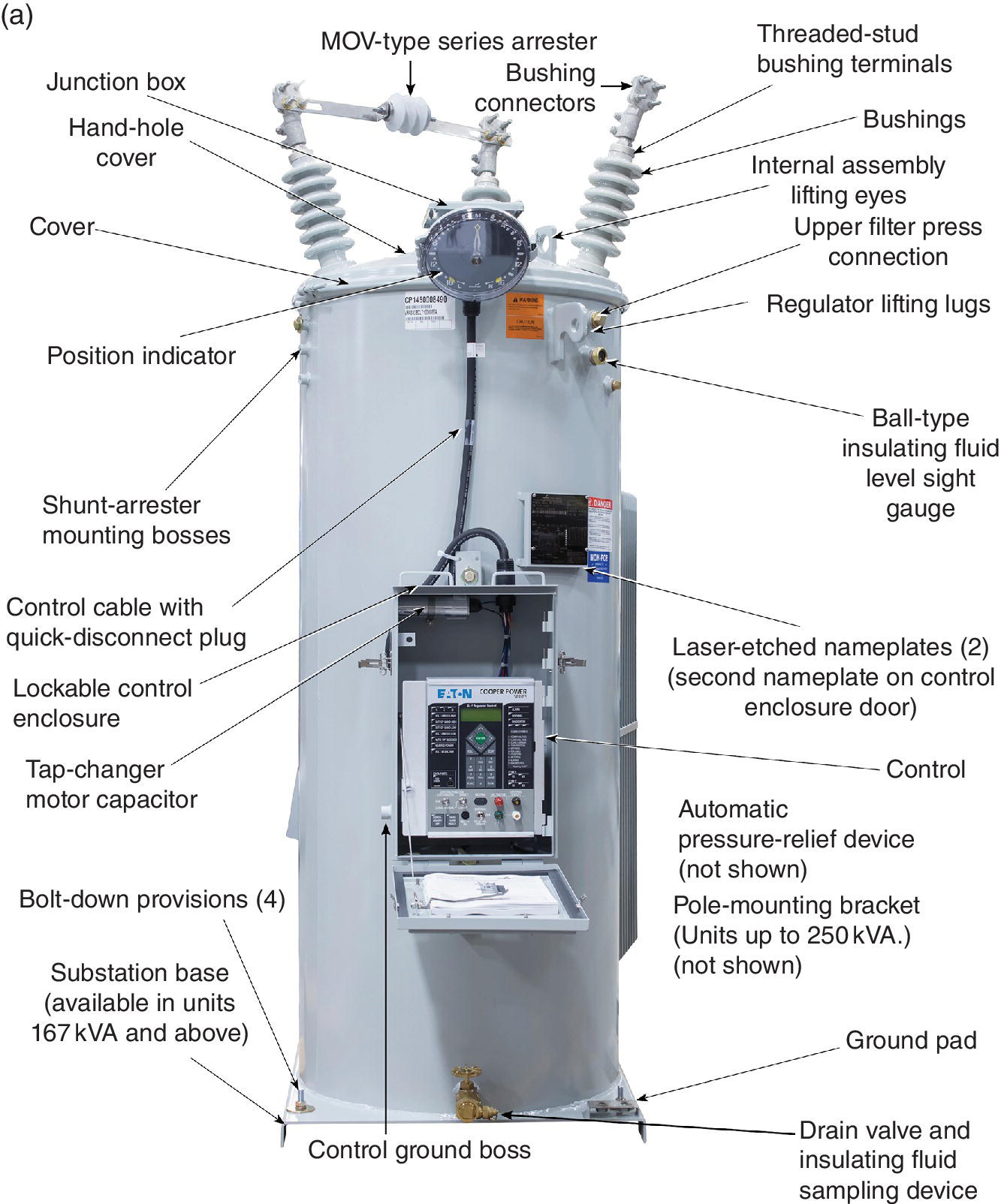

Figure 7.34 (a) Eaton Cooper Power series VR‐32 step voltage regulator.
(Illustration courtesy of Eaton).
Type ‘A’ and ‘B’ Regulators
There are two main variants of the basic step regulator, defined in the American National Standard ANSI C57.15 as Type ‘A’ and Type ‘B’ regulators. They both operate on the same principle and represent years of product refinement. We will investigate a 32‐step Type ‘B’ regulator which provides a regulation range of ±10% of the system line voltage, in 16 steps up of 0.625% and 16 down, in addition to a neutral tap (tap 0), on which the regulator has an effective voltage gain of 1. The fine step size means that regulation action is unlikely to be noticed by customers. Two 22 kV pole‐mounted regulators in an open delta configuration are shown in Figure 7.35.

Figure 7.35 Typical pole‐mounted installation (open delta connection). (Note the pole top bypass and isolation switches).
The regulator’s operating principle is illustrated in Figure 7.36a where a Type ‘A’ regulator is shown. Here the supply voltage VS, is connected across the shunt winding, and the load voltage VL, is obtained across both the series and shunt windings in combination. The series winding is excited by the shunt winding, since they are both wound on the same transformer core. Depending on the position of the reversing switch, the regulator either boosts or bucks the source voltage, yielding an effective turns ratio of ![]() , where Np is the number turns on the shunt winding, and Ns is the number of selected turns on the series winding.
, where Np is the number turns on the shunt winding, and Ns is the number of selected turns on the series winding.

Figure 7.36a Type ‘A’ regulator.
(Adapted and reprinted with permission from IEEE. Copyright IEEE C57.15 (1986) All rights reserved. Permission for further use of this material must be obtained from IEEE. Requests may be sent to: stds‐[email protected]).
Type ‘B’ regulator appears in Figure 7.36b. Here the supply voltage is connected through the tap‐changer and is applied to both the series and shunt windings in combination. The load voltage VL appears across the shunt winding and, depending on the position of the reversing switch, it is either boosted above VS or bucked below it. The turns ratio is given by ![]() .
.

Figure 7.36b Type ‘B’ regulator.
(Adapted and reprinted with permission from IEEE. Copyright IEEE C57.15 (1986) All rights reserved. Permission for further use of this material must be obtained from IEEE. Requests may be sent to: stds‐[email protected]).
As a result of this connection, the shunt winding sees a regulated voltage, and hence its excitation is less variable that of the Type ‘A’ regulator. To raise the load voltage in a Type ‘A’ device, the reversing switch must be in the lower position (Figure 7.36a), while in the Type ‘B’ regulator must be in the upper position (Figure 7.36b).
Thirty‐Two‐Step Voltage Regulator
The schematic diagram in Figure 7.37a provides a simplified view of a thirty‐two‐step voltage regulator. It has three main terminals, S (source), L (load) and SL (source‐load reference terminal). Figure 7.37b shows the regulator applied to a single‐phase line. Here the reference terminal (SL) is connected to the neutral, the source (S) is connected to the incoming phase terminal, and the load terminal (L) supplies potential to the line downstream of the regulator. Bypass and isolation switches (disconnectors) are incorporated into the installation to facilitate removal of the regulator without the need to take the line out of service.


Figure 7.37 (a) Simplified schematic of an Eaton 32 step regulator (b) Single‐phase two‐wire regulator connection.
(Illustrations courtesy of Eaton).
Between the reference (SL) and the load terminal (L) is the shunt winding of the series transformer. On the same magnetic circuit are the series and control windings. The series winding has eight tapping leads and a total voltage equal to 10% of that seen by the shunt winding. A portion of this voltage will be either added or subtracted – through the action of the tap‐changer – to the source potential and delivered to the load terminal. The control winding serves two functions: firstly it acts as a voltage transformer, providing the controller with a representation of the downstream voltage for regulation purposes, and secondly it supplies power for both the tap‐change motor and the control circuitry. Finally, a current transformer provides load current information to the controller. This is used for both power flow and energy measurement, as well as for line drop compensation purposes.
Tap‐Changer
The heart of the regulator is the tap‐changer, and from the schematic diagram in Figure 7.37a it can be seen that there are no separate diverter switches. Instead a combined diverter‐selector switch (also called an arcing switch) is used. This makes the tap‐changer mechanism simpler and more compact, but steps must be taken to minimise any arcing of these contacts. This is especially important because they reside in the general volume of insulating oil, and not in the equivalent of a diverter tank. The phase of the series winding is changed using a conventional reversing switch, which only operates when the tap‐changer is in its neutral position.
Figure 7.38 shows the diverter‐selector switch bridging two adjacent tapping contacts. Notice that an insert has been silver soldered to both the leading and trailing edges of each fixed tapping contact. This material is usually sintered copper and tungsten; as such it presents a hard wearing surface with good resistance to arc erosion, and it effectively performs the function of a diverter switch by being able to cope with minor arcing without sustaining serious damage. The wiping contacts are made from a similar material.

Figure 7.38 Combined diverter‐selector switch.
(Illustration courtesy of Eaton).
In contrast, the reversing switch, shown in Figure 7.39, is much simpler. Since it only switches when the neutral tap is selected and therefore does not interrupt current, it requires no special materials in its construction.

Figure 7.39 Reversing switch.
(Illustration courtesy of Eaton).
The schematic of Figure 7.37a shows the tap‐changer in its neutral position, where the S and L terminals are interconnected. This position must be used when the regulator is to be taken out of service, since this is the only one in which it is safe to close the bypass switch (shown in Figure 7.35). Once the bypass has been closed and the isolation switches have been opened, the regulator can be earthed, and maintenance activities can begin, leaving the line operational.
The schematic also shows that there are eight tapping leads. A centre‐tapped equaliser winding and a split phase reactor are inserted between the two diverter‐selector switches (see Figure 7.40). This configuration suggests that the tap‐changer operates in both bridging and non‐bridging modes, which is indeed the case. Thus there are effectively 16 boost steps and 16 buck steps, in addition to the neutral tap. A tap position indicator displaying the current tap is mounted at the top of the tank. The voltage between adjacent tapping leads on the series winding is 1.25% of the primary voltage and, courtesy of the equaliser winding, the load voltage steps are half this value (0.625%).

Figure 7.40 Tap changer in non‐bridging and bridging positions.
The equaliser winding is a little like the autotransformer discussed earlier, but in this case it is wound on the same core as the series winding. It therefore has a constant potential induced within it, which is set to half the inter‐tap voltage, or 0.625% of the applied primary voltage. The midpoint of this winding is connected to the source terminal, S.
When both diverter‐selector switches are connected to the same tapping lead, the voltage induced in the equaliser winding is dropped across the reactor windings. These are interleaved on two sides of a rectangular magnetic circuit (Figure 7.41), and their tight magnetic coupling ensures that a very low leakage reactance exists between them. The reactor is dimensioned so that a reactive current Ic, equal in magnitude to about half the rated regulator current, circulates through the reactor and equaliser windings in non‐bridging tap positions. Conversely, when the selector switches are bridging two adjacent tapping leads, a current of this magnitude also circulates, but now in the opposite direction.

Figure 7.41 The tap‐changer reactor. (The copper strap connects turns interleaved on one leg with those on the other).
The reactor also ensures that half of the load current (IL/2), flows through each side of the tapping circuit. Therefore the total current flowing in one reactor winding is (IL/2 + Ic), while that in the other is (IL/2 − Ic). For this current sharing to be effective both reactor windings must see the same flux, so they must be tightly coupled and, as previously mentioned, this is an essential element of the reactor’s design. In addition, because the reactor operates close to the line potential, it is mounted on three white support insulators which permit its core to approach this potential as well (Figure 7.41). This substantially reduces its insulation requirements.
It must be remembered that the circulating current is largely reactive, lagging behind the inter‐tap voltage by close to 90°. It therefore also lags the load current by about 60–90°. The load current components flow in opposing directions in the reactor windings as well as in each half of the equaliser winding. Because of this there is no associated flux generated in either of these components and therefore they present no reactive impedance to the flow of load current.
On the other hand, the circulating current is limited by the inductance of the reactor itself, and to achieve the desired impedance, an air gap is incorporated within its core. When either diverter‐selector switch opens, the entire load current commutates to the other, while the circulating current is interrupted. This current change is not as dramatic as interrupting the current flow entirely, and while it leads to some arcing of the contacts, the equaliser winding assists by reducing the voltage that would otherwise be developed across the opening diverter‐selector switch (known as the recovery voltage) by an amount equal to 0.625% of the primary potential. Arcing is further minimised by the swift operation of the tap‐changer. The tap‐changers fitted to 32‐step regulators operate under oil, which assists in quenching the arc, and are generally capable of making a complete tap‐change in about 250 ms, thus minimising the time during which arcing can take place.
Regulator Connections
Step regulators can be installed on two‐, three‐ and four‐wire distribution feeders. We have already seen the single‐phase two‐wire connection. The four‐wire arrangement, shown in Figure 7.42, requires three regulators and a grounded neutral conductor. In this configuration each regulator can operate independently if required, although they are usually operated in a leader‐follower arrangement where two regulators follow the tap‐changes of the third (the lead regulator). The load voltages so produced are in phase with source voltages and any residual current flows in the neutral.

Figure 7.42 (a) Four‐wire wye connection. (b) Phasor diagram. (Illustrations courtesy of Eaton).
Two regulators can also be installed in an open delta configuration on a three‐wire line as shown in Figure 7.43. Here the B phase has been used as the common phase. It can be seen from the phasor diagram that as the A′B and C′B voltages increase, due to the action of the regulator, so the A′C′ voltage increases as well, gaining half its increase from each regulator. For this reason it is important to operate open delta regulators in the leader‐follower mode, ensuring that all line voltages are maintained in step.

Figure 7.43 (a) Two regulator open delta connection (b) Phasor diagram (Illustrations courtesy of Eaton).
One possible disadvantage with the open delta arrangement is the neutral shift voltage that occurs as a result. The neutral voltage lies at the centroid of the line voltage triangle, and since the source and load line phasor triangles are not concentric, there will be a slight shift in the neutral potential of the load side with respect to that of the source. This can cause nuisance tripping of some earth fault protection schemes when lines are paralleled.
On long feeders it may be necessary to install several sets of regulators at intervals along the line. In such cases the neutral shift problem can be partially alleviated if three open delta regulators are installed, each using a different reference phase. The effect is to alter the neutral shift voltage by 120° at each installation so that by the third, the neutral point has returned to its original location. The effectiveness of this technique depends upon the load applied to each regulator installation and the voltage drop along the line between them.
The final arrangement frequently used is the three regulator closed delta connection, illustrated in Figure 7.44. It has the advantage that both the source and load line phasor triangles are concentric and therefore no neutral shift potential exists. It also offers an additional 5% regulation range, so that ±15% of the nominal line voltage can be accommodated.

Figure 7.44 (a) Three regulator, closed delta connection (b) Phasor diagram
(Illustrations courtesy of Eaton).
Although the source and load phasor triangles are concentric, there is a slight phase shift between corresponding source and load voltages. At maximum regulation, this shift is about 5°, as shown in Figure 7.44, and therefore care must be exercised when paralleling feeders downstream of different regulator installations.
Paralleling Autotransformer Based Regulators
Autotransformer based regulators of any type present an impedance that varies roughly as the square of the boost or buck turns inserted into the circuit. Therefore when operating on the neutral tap, a regulator’s impedance is effectively zero. It generally rises from zero to a relatively low value at the maximum boost (or buck) tap available. For example, the maximum impedance presented by an Eaton regulator is only about 0.5%, when the entire series winding is used to either boost or buck the supply voltage. Therefore large and damaging circulating currents will flow between paralleled regulators when operating from different taps, or between paralleled regulators where an inherent phase shift exists between them. For this reason, regulators may only be paralleled if they are each operated in the leader‐follower mode, and are used in conjunction with an external current limiting device. For example, they may be supplied from different transformers, or alternatively they may each have a series current limiting reactor fitted, in order to reduce the magnitude of the circulating currents that will arise during tapping operations.
Sometimes, it is necessary to parallel MV feeders during switching operations. The neutral shift potential created by open delta connections can cause nuisance tripping of earth fault protection schemes. This problem occurs when such feeders are paralleled with others without open delta regulators or with feeders having a different number of open delta regulators. In these cases it is the residual current resulting from the neutral shift voltage between the two lines that is detected by the protection relay.
In order to avoid this problem, it is common practice to place the tap‐changers involved on the neutral tap and leave the regulator in its manual mode, so that no auto‐tapping can occur, before the lines are paralleled. This approach is generally successful, but the line voltage may drift out of limits during switching operations as a result. It is also worth mentioning the need to ensure that the neutral tap is selected before the bypass switch is closed. Failure to do so will result in very high fault currents and severe damage to the unit.
Line Drop Compensation
One useful feature incorporated into the regulator controller is the ability of the device to regulate the voltage at a remote point downstream of the installation; this feature is known as line drop compensation (LDC). This is achieved by modifying the information provided by the voltage transformer at the regulator, to account for the line drop between the regulator and the downstream load centre. Figure 7.45 represents the traditional LDC arrangement.

Figure 7.45 Line drop compensation.
(Illustrations courtesy of Eaton).
In addition to the voltage transformer that senses the downstream potential, the regulator is also equipped with a current transformer in series with the load terminal. This measures the load current flowing, and its secondary current can be made to flow through a miniature replica of the downstream line, located within the controller (shown in Figure 7.45). If the controller’s X and R values are set so that they reflect those of the line, then the voltage sensing circuit will effectively see a potential corresponding to that at the desired downstream location. The regulator will therefore control the potential there, at the expense of a slightly higher line voltage at the regulator itself. Modern regulator controllers usually perform the LDC calculations digitally, although they still require the user to specify the X and R settings corresponding to that portion of the feeder downstream of the regulator.
Reverse Modes of Operation
In most applications the regulator will be installed on a line where the power flow is unidirectional, and in these cases regulation will always be applied towards the load side. However, on some lines the power flow may reverse from time to time, and in such cases it is desirable that the direction of regulation does so as well. (This requirement occurs more frequently nowadays with the increased penetration of renewable power sources in the distribution network, including wind and photovoltaic distributed generation.) This requires that the controller be able to determine the power flow direction, and apply the regulation to the source side rather than the load side. The latter requires that the source voltage be used as the reference for regulation; however, since the voltage transformer is located on the load side, steps must be taken to enable the regulator to obtain source voltage information. This may be done by installing as second voltage transformer on the source side, or in the case of some controllers, the source voltage can be obtained from the load voltage by knowing the tap selected, the current flowing and the impedance of the series winding.
There are six modes of reverse operation provided in Eaton regulator controllers. In the bidirectional mode the controller measures the power flow along the line and thus determines the magnitude and direction of the current. Should the current exceed the reverse direction threshold, the controller will then use the source voltage as its reference, and the regulator’s operation will switch towards the source, regulating this potential instead.
7.10 Problems
- Consider Equations (7.3) and (7.4). What options are available to a designer wishing to build a high impedance transformer, i.e. one with a high X/R ratio?
- Phase shifting transformer or phase angle regulator (PAR). Figure 6.12 shows a 132 kV:132 kV, 200 MVA phase shifting transformer, whose nameplate appears in Figures 7.46 and 7.47. It was installed on an Australian transmission line running between Armidale and Kempsey. Armidale is one of the substations that receive a strong in‐feed when energy is imported into New South Wales from Queensland. During such times, this line frequently becomes overloaded and in order to prevent this, the power imported must be reduced accordingly. In order to remove this constraint a phase shifting transformer was installed.

Figure 7.46 Phase shift transformer nameplate.

Figure 7.47 Phase shift transformer nameplate, continued.
By regulating the phase shift across this transmission line, the power flowing through it can be controlled. This transformer can vary the phase at one end of the line and therefore influence the power flowing in the line without appreciably altering the local Armidale bus voltage.
The transformer in Figure 6.12 is actually a composite transformer, consisting of two tanks each containing a transformer and tap‐changer. The main transformer is in one tank and the series transformer in the other. Between them are two cabling ducts, as shown in plan view in Figure 7.46.
The main transformer is a star‐star connected 132 kV:132 kV transformer with a tertiary delta winding, as shown in Figure 7.47. Its primary (source) terminals are S1, S2 and S3 and its tap‐changer is capable of regulating the voltage at the load terminals L1, L2 and L3. The tertiary winding associated with this also provides excitation to the series transformer, located in the other tank. The local bus is connected to terminals S1, S2 and S3 and the transmission line to be controlled is fed by terminals L1, L2 and L3.
The series transformer is also a star‐star connected device with a tertiary delta winding (see Figure 7.47). Its secondary and tap‐changer windings are connected in series with the source windings of the main transformer, but because of the interconnections between the two transformers, the series voltages are in quadrature with the source voltages of the main transformer.
Phase regulation: The series transformer’s tap‐changer has the ability to regulate both the sign and magnitude of the voltage at terminals X, Y and Z in Figure 7.47. As a result the voltage applied to the main transformer primary windings can be varied in phase with respect to that of the local bus. This phase shift is achieved by adding a small quadrature voltage to each of the main transformer’s primary windings, as shown in Figure 7.48.

Figure 7.48 Quadrature phase shifting.
The quadrature voltages are applied between neutral end of the main primary windings and the star point. They are generated by the series transformer, and appear at terminals X, Y and Z.
As shown, the quadrature voltages can be altered in magnitude (and sign) by the tap‐changer associated with the series transformer. By using a tap‐changer reversing winding and changeover switch, shown in Figure 7.47, it is possible for the tap‐changer voltage to either buck or boost that in the fixed windings X, Y and Z. For example, if the reversing switch is in position P0‐P2 then the tapping winding bucks the fixed winding, and thus it is possible that at one particular tap position, for the voltages at Z, Y and Z to become zero. An inspection of the tapping chart shows that this occurs on tap 20. When the quadrature voltages are zero there will be no induced phase shift between the supply and the load voltages. The phase shift tapping chart confirms this. Tap 20 is therefore the null tap.
In the buck condition described above, should the tapping winding voltage exceed that of the fixed winding, then the quadrature voltage will change sign, and with it the sign of the phase shift angle as well. In this case the load voltage will lead that at the source terminals. The tapping chart also demonstrates this. (In this case, lagging angles are defined as negative and leading angles are positive.)
On the other hand, when the tap‐changer boosts the voltage in windings X, Y and Z the quadrature voltage will become larger, and with it the induced phase shift as well. As shown in Figure 7.48, this will result in a lagging phase shift between the primary voltage of the main transformer and the applied bus voltage. Because the load windings are also wound on the main transformer, the load voltage will also lag the applied voltage by the angle δ.
Voltage regulation: Figure 7.48 shows that, as the phase of the primary winding voltage is changed, unfortunately so is its magnitude. Changes in magnitude of the load voltage will affect the VAr flow and to a lesser extent the power flow as well. In order to prevent this, the load voltage must generally be held constant. This is the task of the voltage tap‐changer associated with the load windings L1, L2 and L3. Thus in normal operation, the phase shift through the transformer will be set using the phase tap‐changer – to achieve the desired power flow – and the resulting load voltage will be held constant by the voltage tap‐changer. Tap 5 is the null tap on the voltage tap‐changer, since the load voltage here is 132 kV.
Transformer under load: The tapping charts assume that a source voltage of 132 kV is applied and that the transformer is not loaded. The adjustment of phase angle table in the upper part of Figure 7.46 shows that the induced phase shift also becomes more lagging when the transformer is inductively loaded. The equivalent circuit in Figure 7.49 can be used to demonstrate this effect, which shows that the load voltage under zero current conditions (VL*) is given by the sum of the supply and quadrature components (VS and Vq), as described already.

Figure 7.49 Equivalent circuit of phase shifting transformer. (VL* = Load voltage when IL = 0, VS = source voltage and Vq = quadrature voltage).
When the transformer is inductively loaded at an angle ϕ, the terminal voltage VL, lags VL* by an additional angle δ′, as shown in Figure 7.50.

Figure 7.50 Effect of a lagging load current I on the terminal voltage VL.
Finally, Figure 7.51 shows the combination of a leading phase shift between VL and VS, induced by the quadrature voltage and the lagging effect produced by the combined effect of the load current and the transformer’s impedance, X.

Figure 7.51 Overall phase shift becomes more lagging as a result of load current, I.
Questions:
- Why will phase control regulate the power flow on a transmission line? Explain.
- By using of phasor diagrams, show how the quadrature voltages discussed above are generated for each phase. (You will need to consider the main and series transformer interconnections shown in Figure 7.47.)
- From the voltage information in the tapping table, estimate the voltage induced in the phase shift windings X, Y and Z, when the applied bus voltage is 132 kV. (The tapping charts always assume that the nominal bus voltage is applied, i.e. 132 kV.)(Answer: 27.47 kV, each phase tap corresponds approximately to 3.9 kV.)
- Calculate the phase shift generated when the tap‐changer is in position 9. Compare this result with the tapping chart.(Answer: 18.48°)
- Calculate the resulting load winding voltages for this condition. Assume that the transformer is unloaded. Compare your result with the tapping chart. (Neglect any compensation from the voltage tap‐changer.)(Answer: 125.2 kV)
- Which tap should be selected from the voltage tap‐changer in order to restore the load voltage to 132 kV?(Answer: Either tap 9 or 10)
- The phase shift table in Figure 7.46 shows that a maximum leading phase shift of 8.64° can be achieved when the transformer is unloaded. Using the equivalent circuit of Figure 7.51, calculate the maximum leading phase shift that you expect from the transformer when it is supplying its rated load at a power factor of 0.95. You will need to know the transformer’s impedance. Compare your result with that given in Figure 7.46.(Answer: Max leading angle = 1.82°)
- Out‐of‐step transformer operation. In this question we consider the out‐of‐step operation of a pair of transformers, T1 and T2. To simplify our analysis we will neglect the resistive component of each transformer’s impedance, and we will assume that the magnitude of the reactive component is independent of the tap position. The single‐phase equivalent circuit of these transformers appears in Figure 7.52. The load impedance is assumed to be 1.0 pu, with a lagging power factor of 0.966 and it is connected to a bus whose voltage, VB is 1 pu. These high impedance transformers are identical, each with a reactance X = 0.33 pu.
- We begin with the transformers operating from the same tap. Draw the phasor diagram for the bus voltage, VB the reactive drop (Vx) and obtain from it the open circuit secondary voltages, E1 and E2, and the power angle δ. Assume that each transformer supplies half the load current. Hint: Make VB the reference phasor, and use a scale of 1.0 pu = 300 mm and calculate the power angle from the dimensions of your drawing, don’t measure it directly.(Answer: E1 = E2 = 1.055 pu, δ ≈ 8.2°.)
- Assume that we now adjust the taps on the transformers so that E1 is increased by 5% and E2 is reduced by 5%. Since these changes are symmetrical with respect to VB we might assume that VB remains largely unaltered. In addition, the voltages E1 and E2 must remain in phase. (Why?) Modify your phasor diagram to show this, and from it evaluate the new transformer currents I1 and I2.(Answer: I1 = 0.586 pu, I2 = 0.454 pu.)
- From your phasor diagram, calculate the phase angles between the bus voltage and I1 and I2 respectively. Calculate also the values of P and Q delivered by each transformer to the load. Show that these quantities are consistent with the power delivered to the load. Why has the tap‐change affected Q more than P? (Answer: θ1 ≈ 29.7°, θ2 ≈ −3.7°, P1 ≈ 0.46 pu, P2 ≈ 0.45 pu, Q1 ≈ 0.291 pu, Q2 ≈ −0.034 pu) The unbalance is due to a significant circulating current that leads to high reactive power losses.Calculate the total reactive power each primary winding must provide under the tap settings of part 2. Where is the extra reactive power consumed?(Answer: Q1pri = 0.40 pu, Q2pri = 0.035 pu)
- Modify your phasor diagram to include the circulating current, Ic, shown in Figure 7.53. Does this provide a partial justification of our initial assertion that E1 and E2 should lie in phase? Explain. What magnitude do you expect for Ic? Why must this current exist? Hint: What phase relationship do you expect between Ic and (E1 – E2)?(Answer: Ic = 0.162 pu.)
- If T2 is now taken out of service, with its present tap settings, what value would the bus voltage adopt? (Assume that the load impedance remains unchanged.) If T1 is taken out of service instead, how would VB change? In the light of this information, devise an operational procedure that you might use as a system operator, for the purpose of taking one of a pair of transformers out of service.(Answer: 0.98 pu (T2 off), 0.88 pu (T1 off).)

Figure 7.52 Single‐phase equivalent circuit.

Figure 7.53 Inclusion of the circulating current, ic.
- A new 11,000 V:433 V Dyn11 transformer has been installed to share an LV load with an existing transformer of the same vector group, but initially the pair were not operating from the same tap. The original transformer was on the 11550 V:433 V tap and the new transformer was installed on its principal tap (11,000 V:433 V). The data relating to these transformers, measured at the connection to the bus, appears in the table below. The load voltage in this configuration was 422 volts.
Rating Impedance Supply voltage P (kW) Q (kVAr) Existing transformer 1 MVA 11.56% 11 kV 230 –220 New transformer 1 MVA 8.75% 11 kV 320 344 Tappings: 10,450 V:433 V, 10,725 V:433 V, 11,000 V:433 V, 11,275 V:433 V, 11,550 V:433 V 11,825 V:433 V 12,100 V:433 V.
- By making any reasonable assumptions, and assuming that the impedance values quoted are wholly inductive and include the transformer, the LV cable and bus connections, calculate the power angle δ.(Answer δ ≈ 1.4°)
- Calculate the magnitude of the reactive current circulating between these transformers.(Answer: ≈ 300 A.)
- Calculate the load impedance, assuming it to be represented by a resistive element in parallel with an inductive one.(Answer: 0.324 + j1.63 ohms)
- Assuming that the load impedance remains constant, determine the tap setting for the new transformer which will see the load shared most evenly between the two. You may assume that the transformer impedances do not vary appreciably with tap setting.(Answer: 11,825 V:433 V)
- Most MV‐LV distribution transformers are of the Dyn11 vector grouping. Under what conditions would a Zyn11 transformer be an acceptable substitute and why?
- Show by constructing a suitable phasor diagram, that a phase shift of about 5° arises between corresponding source and load voltages in the three regulator closed delta configuration shown in Figure 7.44.
7.11 Sources
- 1 Say MG. ‘Alternating current machines’, 2nd ed, 1976, Pitman Press, London.
- 2 IEEE Std C57.131 ‘IEEE standard requirements for tap‐changers’, 2012, IEEE Power Engineering Society, New York.
- 3 IEC 60076‐1 ‘Power transformers – Part 1 General’, 2011, IEC International Electrotechnical Commission, Geneva.
- 4 IEEE Std C57.15. Requirements, terminology and test code for step voltage and induction‐voltage regulators’, 1988, IEEE Power Engineering Society, New York.
- 5 AS 60214.1 ‘Tap changers part 1; Performance requirements and test methods’, 2005, Standards Australia, Sydney.
- 6 Harlow JH. ‘Load tap‐changing control’ Beckwith Electric Co, Largo FL 34649.
- 7 Sankar V. ‘Preparation of transformer specifications’ Power Engineering Society Industry Application Seminar 2012; IEEE Power Engineering Society, New York.
- 8 Jonsson L, Sundqvist D. ‘Vacuum interrupters as an alternative to traditional arc quenching on‐load tap‐changers’ ABB Sweden, TechCon Asia Pacific; 2007.
- 9 Harlow JH. ‘Transformer tap‐changing under load a review of concepts and standards’, 1993, Beckwith Electric Co, Largo FL 34649.
- 10 Beckwith Electric Co ‘Introduction to paralleling of LTC transformers by the circulating current method’ Application note 11, Beckwith Electric Co, Largo FL 34649.
- 11 Jauch E.T. ‘Advanced transformer paralleling’ 2001, IEEE Power Engineering Society, New York.
- 12 Areva T&D ‘Network protection & automation guide’, 2005 Edition, Areva T&D, Paris.
- 13 Kloss A. ‘A guide to power electronics’ 1984, John Wiley & Sons, Chichester.
- 14 Schaffer J. ‘Rectifier circuits, theory and design’ 1965, John Wiley & Sons, New York.