Chapter 3
Putting Logic Circuits to Work
In This Chapter
![]() Implementing logic gates with transistors
Implementing logic gates with transistors
![]() Looking at TTL and CMOS integrated circuits
Looking at TTL and CMOS integrated circuits
![]() Building simple logic circuits
Building simple logic circuits
In this chapter you get the chance to work with circuits using the popular logic gates that we introduce in this minibook’s Chapter 2. We show you the basics of creating logic gates from simple transistor circuits and look at two popular integrated circuit (IC) families that provide prebuilt logic gates: transistor-transistor logic and complementary metal-oxide semiconductor logic, which sound less intimidating when abbreviated to TTL and CMOS.
 Unless you’re already well up-to-speed on logic gates, we suggest that you read Chapter 2 of this minibook before tackling the projects in this chapter. It isn’t going to make much sense if you aren’t familiar with the different types of gates we describe in that chapter.
Creating Logic Gates with Transistors
In Book II, Chapter 6, we discuss how you can use transistors as switches (if you want to know how transistors work, check out that chapter). In a nutshell, a voltage applied to the base of a transistor allows current to flow from the collector to the emitter. Thus, by applying an input signal to a transistor’s base, you can control an output signal taken from the collector-emitter path.
You can build any logic gate you want by cobbling together a few transistors and resistors in just the right way. In this section, we look at simple transistor circuits for five gate types: NOT, AND, OR, NAND and NOR.
 All the circuits in this chapter assume that a high signal (logical 1) is represented by a DC voltage of +5 V or more. Low (logical 0) is represented by near-zero voltage. This minibook’s Chapter 1 has more details on these terms.
Note that you don’t often build your own logic gates with transistors and resistors. Instead, you use ICs that contain prefabricated logic gates. But before you use logic ICs in your circuits, you need to have a basic understanding of how the gates inside them work. So we recommend that you take a look at simple transistor circuits for basic logic gates, and then examine the logic ICs in the later ‘Introducing Integrated Circuit Logic Gates’ section.
Discovering a transistor NOT gate circuit
A NOT gate simply inverts its input. If the input is high, the output is low, and if the input is low, the output is high. Such a circuit is easy to build using a single transistor and a pair of resistors. Figure 3-1 shows the schematic. The bar over the output is a common notation to indicate ‘NOT’.

Figure 3-1: A transistor NOT gate.
The operation of this circuit is simple. The input is connected through resistor R2 to the transistor’s base. When no voltage is present on the input, the transistor turns off. When the transistor is off, no current flows through the collector-emitter path. Thus, current from the supply voltage (Vcc in the schematic, typically between +5 V and +9 V) flows through resistor R1 to the output. In this way, the circuit’s output is high when its input is low.
When voltage is present at the input, the transistor turns on, allowing current to flow through the collector-emitter circuit directly to ground, which causes the output to go low.
In this way, the output is high when the input is low and low when the input is high.
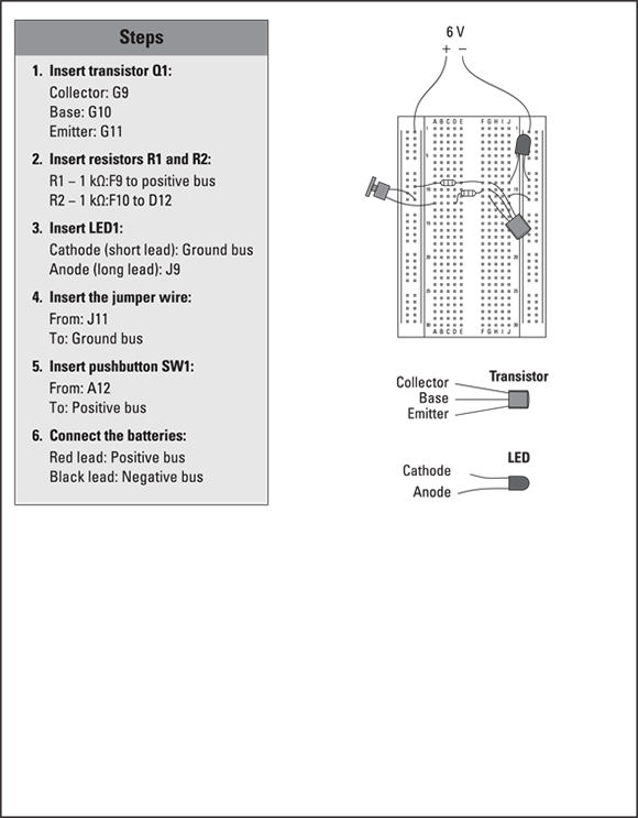
Project 3-1 demonstrates how to assemble a simple transistor NOT gate on a solderless breadboard. For this project, a normally open pushbutton is used as the input. When the button isn’t pressed, the input is low and the output is high, which causes the light-emitting diode (LED) to light. When you press the button, the input goes high, the output goes low and the LED goes out. Figure 3-2 shows the assembled project.

Figure 3-2: A transistor NOT gate assembled on a breadboard (Project 3-1).

Going high with a transistor AND gate circuit
A two-input AND gate produces a high output if both inputs are high. You can create a two-input AND gate by using two transistors and three resistors, as shown in Figure 3-3. In this circuit, the output current has to flow from the Vcc supply voltage through the collector-emitter circuits of both transistors to reach the output. Thus, current flows to the output only if both transistors are on.
The bases of both transistors are fed through R2 and R3 from the two inputs. So if both inputs are high, current flows through the base-emitter path of both transistors, turning them on and allowing current to flow through to the output. If either input is low, the corresponding transistor turns off and the output goes low.

Figure 3-3: A transistor AND gate.
Staying low with a transistor NAND gate circuit
A two-input NAND gate produces a low output if both its inputs are high. Although you can create a NAND gate by combining the circuits shown in Figure 3-1 and Figure 3-3, so that the output from the AND gate is used as input to the NOT gate, that combination requires three transistors. In fact, creating a NAND gate using just two transistors is pretty easy, as shown in Figure 3-4.

Figure 3-4: A transistor NAND gate.
 This NAND gate circuit is almost identical to the AND gate circuit shown in the earlier Figure 3-3. The only difference is that instead of connecting the output to the emitter of the second transistor, the output is obtained before the collector of the first transistor. If both inputs are high, both transistors conduct through their collector-emitter paths, which creates a short circuit to ground and in turn causes the output to go low.
If either transistor turns off, however, the supply current can’t flow through the transistors to ground, and so it flows through the output circuit instead. Thus, the output is high if either one of the inputs is low. If both inputs are high, the output is low.
Project 3-2 shows you how to assemble a simple transistor NAND gate on a solderless breadboard. Normally open pushbuttons are used for the two inputs. The LED is on until you press both the pushbuttons. This action causes both inputs to go high, which causes the output to go low and the LED to go dark. The completed project is shown in Figure 3-5.
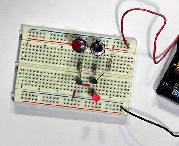
Figure 3-5: A two-transistor NAND gate on a breadboard (Project 3-2).


Looking at a transistor OR gate circuit
A two-input OR gate produces a high output if either input is high or both its inputs are high. Figure 3-6 shows a schematic for an OR gate created with two transistors and three resistors.

Figure 3-6: A transistor OR gate.
In the OR gate circuit, the supply voltage is connected separately to the collector of each transistor. Then the emitters of both transistors are connected to the output. That way, if voltage is applied to the base of either one of the transistors, that transistor turns on and passes current through to the output.
Thus, the output is high if one input is high or both inputs are high. The output is low only if both inputs are low.
Knowing about transistor NOR gate circuits
A NOR gate is an inverted OR gate. If at least one of the inputs is high, the output is low. If both inputs are low, the output is high.
Figure 3-7 shows a schematic for a NOR gate. This circuit is similar to the circuit shown in Figure 3-6 in the preceding section, except that the output is connected to the collector of both transistors and the emitter of each transistor is connected to ground. If either one of the transistors is on, current from Vcc is short-circuited to ground, bypassing the output. As a result, the output is high only when both inputs are low. If either input is high or both inputs are high, the output is low.

Figure 3-7: A transistor NOR gate.
You can build a two-transistor NOR gate by following the steps outlined in Project 3-3. As with the other projects in this chapter, Project 3-3 uses normally open pushbuttons to control the input circuits. When power is applied to this circuit, both inputs are initially low and the output is high. Pressing either one of the switches causes that switch’s input to go high, which in turn causes the output to go low. The assembled project is shown in Figure 3-8.

Figure 3-8: A two-transistor NOR gate on a breadboard (Project 3-3).


Introducing Integrated Circuit Logic Gates
Although you can build your own logic gates using transistors and resistors as we describe in the preceding sections, buying prepackaged ICs that implement logic gates is far easier. The main advantage of using IC logic gates is that you don’t have to design the individual gates yourself or waste time assembling them.
The logic gate circuits in the preceding sections are among the simplest circuits for creating logic gates, but they’re by no means the only ways to create logic gates – and not necessarily the best. Over the 50 years or so that circuit designers have been working on semiconductor-based logic circuits, many designs have been developed for creating logic gates.
Each approach to designing logic circuits results in an entire family of logic circuits for the various types of gates (NOT, AND, OR, NAND, NOR, XOR and XNOR), and for this reason the different designs are often referred to as design families. Each family has an easy-to-remember three- or four-letter acronym. Here are the most popular:
![]() RTL: Resistor-transistor logic, which uses resistors and bipolar transistors. The circuits we present in the preceding sections are examples of RTL circuits.
RTL: Resistor-transistor logic, which uses resistors and bipolar transistors. The circuits we present in the preceding sections are examples of RTL circuits.
![]() DTL: Diode-transistor logic, which is similar to RTL but adds a diode to each input circuit.
DTL: Diode-transistor logic, which is similar to RTL but adds a diode to each input circuit.
![]() TTL: Transistor-transistor logic uses two transistors, one configured to work as a switch and the other configured to work as an amplifier. The switching transistor is used in the input circuits and the amplifier transistor is used in the output circuits. The amplifier allows the gate’s output to be connected to a larger number of inputs than RTL or DTL circuits.
TTL: Transistor-transistor logic uses two transistors, one configured to work as a switch and the other configured to work as an amplifier. The switching transistor is used in the input circuits and the amplifier transistor is used in the output circuits. The amplifier allows the gate’s output to be connected to a larger number of inputs than RTL or DTL circuits.
In a TTL circuit, the switching transistors are special transistors that have two or more emitters. Each input is connected to one of these emitters so that the separate inputs all control the same collector-emitter circuit. The switching transistor’s base is connected to the Vcc supply voltage and the collector is connected to the base of the amplifying transistor. Figure 3-9 shows a typical TTL circuit.
Although you can build TTL circuits using individual transistors, ICs with TTL circuits are readily available. The most popular types of TTL ICs are designated by four-digit numbers starting with ‘74’. Several hundred types of 7400-series ICs are available, though many provide advanced logic circuits that you aren’t likely to use for home electronics projects.

Figure 3-9: A typical TTL gate.
The ICs listed in Table 3-1 provide several basic logic gates in a single package. Quad means ‘four’ in the first part listed; hex means ‘six’ in the third part and, as we explained in the preceding chapter, a NOT gate is also known as an inverter.
![]() CMOS: Complementary metal-oxide semiconductor logic refers to logic circuits built with a special type of transistor called a metal oxide semiconductor field effect transistor (fortunately known as MOSFET for short). The physics of how a MOSFET differs from a standard bipolar transistor aren’t all that important unless you want to become an IC designer. What is important is that MOSFETs use much less power, can switch states much faster and are significantly smaller than bipolar transistors. These differences make MOSFETs ideal for modern IC, which often require millions of transistors on a single chip.
CMOS: Complementary metal-oxide semiconductor logic refers to logic circuits built with a special type of transistor called a metal oxide semiconductor field effect transistor (fortunately known as MOSFET for short). The physics of how a MOSFET differs from a standard bipolar transistor aren’t all that important unless you want to become an IC designer. What is important is that MOSFETs use much less power, can switch states much faster and are significantly smaller than bipolar transistors. These differences make MOSFETs ideal for modern IC, which often require millions of transistors on a single chip.
Table 3-1 7400-Series TTL Logic Gates
|
Number |
Description |
|
7400 |
Quad two-input NAND gate (four NAND gates) |
|
7402 |
Quad two-input NOR gate (four NOR gates) |
|
7404 |
Hex inverter (six NOT gates) |
|
7408 |
Quad two-input AND gate (four AND gates) |
|
7432 |
Quad two-input OR gate (four OR gates) |
|
7486 |
Quad two-input XOR gate (four XOR gates) |
Apart from drawing less power and operating more quickly than TTL circuits, CMOS circuits work much like TTL circuits. In fact, CMOS chips are designed to be interchangeable with comparable TTL chips.
CMOS logic chips have a four-digit part number that begins with the number ‘4’ and so are often called 4000-series chips. As with the 7400 series of TTL logic chips, several hundred types of 4000-series chips are available. Table 3-2 lists the ones that provide basic logic gates.
Table 3-2 4000-Series CMOS Logic Gates
|
Number |
Description |
|
4001 |
Quad two-input NOR gate (four NOR gates) |
|
4009 |
Hex inverter (six NOT gates) |
|
4011 |
Quad two-input NAND gate (four NAND gates) |
|
4030 |
Quad two-input XOR gate (four XOR gates) |
|
4071 |
Quad two-input OR gate (four OR gates) |
|
4077 |
Quad two-input XNOR gate (four XNOR gates) |
|
4081 |
Quad two-input AND gate (four AND gates) |
 CMOS logic circuits are very sensitive to static electricity. As a result, take special precautions when you handle them. Make sure that you discharge yourself properly by touching a grounded metal surface before you touch a CMOS chip. For maximum protection, wear an antistatic wrist band. For more information about static precautions, refer to Book I, Chapter 4.
The following sections describe several popular 4000-series ICs and present a few projects that use them.
Making use of the versatile 4000-series logic gates
The 4000-series CMOS logic circuits include ICs that provide several logic gates in a single package. Figure 3-10 shows the pinout connections (a schematic of what each input and output pin does) for six popular 4000-series chips. Each of these six chips contains four two-input logic gates in a 14-pin DIP (that is, a dual in-line package). Power, which can range from +3 V to +15 V, is connected to pin 14, and ground is connected to pin 7.
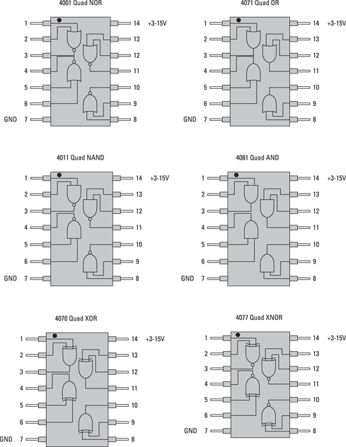
Figure 3-10: Pinout chart for 4000-series quad two-input logic gate chips.
The 4001 and 4011 chips contain four NOR and NAND gates respectively, and because they’re universal gates you can use them in combination to create other types of gates. So make sure that you stock up on 4001 or 4011 chips so that you can create any type of logic circuit you need.
Before you start building circuits with CMOS logic chips, here are a few tips for working with 4000-series chips:
![]() The outputs can source as much as 10 milliamperes (mA) with a 9 V power supply. At 6 V, the maximum is about 5 mA, which is just enough to light an LED.
The outputs can source as much as 10 milliamperes (mA) with a 9 V power supply. At 6 V, the maximum is about 5 mA, which is just enough to light an LED.
If your output circuit requires more current, you can always use a transistor. Just connect the transistor’s collector to the positive voltage source and the base to the logic gate output. Then connect your output circuit to the transistor’s emitter. The output circuit has eventually to lead to ground, of course, to complete the circuit.
![]() The input pins of CMOS logic chips are notorious for picking up stray signals in the form of electrical noise. Although you don’t need to do so in experimental breadboard circuits, in a real-world circuit you have to connect all unused input pins to the positive supply voltage or to ground. (You don’t need to connect the unused outputs to anything – just the inputs.)
The input pins of CMOS logic chips are notorious for picking up stray signals in the form of electrical noise. Although you don’t need to do so in experimental breadboard circuits, in a real-world circuit you have to connect all unused input pins to the positive supply voltage or to ground. (You don’t need to connect the unused outputs to anything – just the inputs.)
![]() In addition to connecting unused inputs to positive voltage or ground, a good idea is to place a small capacitor (47 nF is typical) across the power leads (pins 7 and 14). This capacitor helps to ensure that the input voltage stays constant.
In addition to connecting unused inputs to positive voltage or ground, a good idea is to place a small capacitor (47 nF is typical) across the power leads (pins 7 and 14). This capacitor helps to ensure that the input voltage stays constant.
![]() Don’t forget that CMOS chips are very susceptible to damage from small amounts of static electricity. Be sure to ground yourself by touching a metal object before you touch CMOS chips.
Don’t forget that CMOS chips are very susceptible to damage from small amounts of static electricity. Be sure to ground yourself by touching a metal object before you touch CMOS chips.
Building projects with the 4011 Quad Two-Input NAND Gate
The 4011 Quad Two-Input NAND Gate is a popular CMOS logic gate IC. As its name suggests, this IC contains four two-input NAND gates. The earlier Figure 3-10 illustrates its pinouts, along with those for several other quad two-input gate chips.
You can purchase a 4011 IC at Maplin or online from any of the large electronic component distributors such as Farnell (http://uk.farnell.com/), RS Components (http://uk.rs-online.com) or Digi-Key (www.digikey.co.uk). Make sure you order one in a DIP package for breadboard insertion rather than a surface-mount package for production printed circuit boards.
As we describe in this minibook’s Chapter 2, NAND gates (along with NOR gates) are universal gates, which means that you can construct any other type of gate using nothing but NAND gates combined in various ways. Projects 3-4 to 3-7 walk you through the step-by-step process of building various types of gate circuits using only NAND gates:
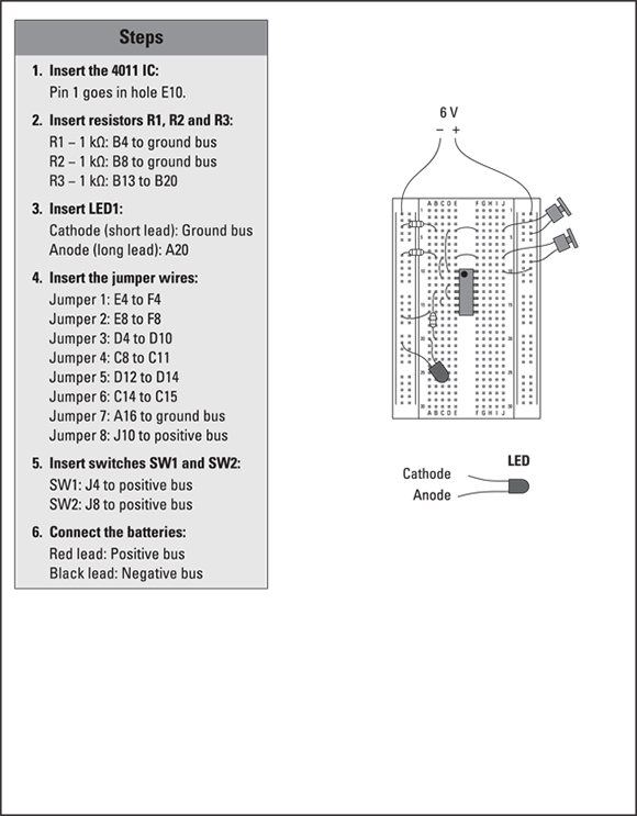
![]() Project 3-4 uses just one NAND gate in a 4011. The two inputs of the NAND gate are connected to pushbuttons and the output is connected to an LED. When you build this project, you can visualise the operation of a NAND gate: the LED is on unless you press both buttons.
Project 3-4 uses just one NAND gate in a 4011. The two inputs of the NAND gate are connected to pushbuttons and the output is connected to an LED. When you build this project, you can visualise the operation of a NAND gate: the LED is on unless you press both buttons.
Figure 3-11 shows Project 3-4 assembled on a solderless breadboard. This figure gives you a good idea of how to connect the components to the breadboard. The project description itself provides detailed instructions. The circuits for Projects 3-5, 3-6 and 3-7 are similar enough in appearance that you can use Figure 3-11 as a guide for the overall appearance of your finished projects.

Figure 3-11: A NAND gate circuit that uses a CMOS logic chip (Project 3-4).
![]() Project 3-5 uses two NAND gates on the 4011 to create an AND gate. Because a NAND gate is nothing more than an AND gate whose output is inverted, you can create an AND gate from a NAND gate by inverting the NAND gate’s output.
Project 3-5 uses two NAND gates on the 4011 to create an AND gate. Because a NAND gate is nothing more than an AND gate whose output is inverted, you can create an AND gate from a NAND gate by inverting the NAND gate’s output.
This inversion works because of a fundamental rule of logic: if you invert a value twice, you get the original value. Thus, if you invert an AND gate once, you get a NAND gate; if you invert it again, you’re back to an AND gate.
Luckily you can easily turn a NAND gate into a single-input inverter (that is, a NOT gate) by connecting the single input to both inputs of the NAND gate. This connection causes the two inputs to always be the same: either both are high or both are low. In a NAND gate, if both inputs are high, the output is low, and if both inputs are low, the output is high. Thus, wiring the inputs of a NAND gate together has the effect of inverting the input.
![]() Project 3-6 shows you how to create an OR gate using three NAND gates. As Chapter 2 of this minibook explains, a NAND gate is the same as an OR gate whose inputs are inverted. Therefore, to create an OR gate using NAND gates, you invert the two inputs with the NAND gates configured as inverters (that is, with their inputs wired together). The output from these inverters is sent to the inputs of the third NAND gate.
Project 3-6 shows you how to create an OR gate using three NAND gates. As Chapter 2 of this minibook explains, a NAND gate is the same as an OR gate whose inputs are inverted. Therefore, to create an OR gate using NAND gates, you invert the two inputs with the NAND gates configured as inverters (that is, with their inputs wired together). The output from these inverters is sent to the inputs of the third NAND gate.
![]() Project 3-7 uses all four NAND gates on the 4011 chip to create a NOR gate, which is nothing more than an OR gate whose output is inverted. Thus, you create an OR gate by using the technique in Project 3-6 and then configure the fourth NAND gate on the 4011 chip as an inverter to invert the output of the OR gate.
Project 3-7 uses all four NAND gates on the 4011 chip to create a NOR gate, which is nothing more than an OR gate whose output is inverted. Thus, you create an OR gate by using the technique in Project 3-6 and then configure the fourth NAND gate on the 4011 chip as an inverter to invert the output of the OR gate.
These projects build on one another, and so don’t tear down your breadboard after completing each project. Instead, use each assembled project as a starting point for the next one. If you build the projects in this way, you can simply scan the steps to see what resistors and jumper wires need to be moved for each project. (The 4011 IC itself, the LED and the two switches are in the same locations for all four projects.)