Chapter 5
Reading Schematic Diagrams
In This Chapter
![]() Depicting circuits in simplified diagrams
Depicting circuits in simplified diagrams
![]() Introducing common component symbols
Introducing common component symbols
![]() Representing voltage supply and common ground circuits
Representing voltage supply and common ground circuits
![]() Seeing how components are typically labelled
Seeing how components are typically labelled
You come across many different types of maps: roadmaps to take on holiday, political maps of the countries of the world and geological maps of underlying rocks, to mention just a few. When you think of a map, you may well visualise a bird’s eye view, showing the precise distances and physical relationships between places, features and landmarks.
Yet one of the world’s most famous, useful and influential maps doesn’t do that at all. Harry Beck’s colour-coded diagrammatic map of the London Underground doesn’t depict exact locations or distances, but focuses instead on the important aspects of the order and connections (check out the nearby sidebar ‘Finding your way underground’).
Electronics uses its own form of map: the schematic diagram. Like Beck’s map these diagrams show how all the different parts that make up an electronic circuit are connected, instead of attempting to show an accurate bird’s eye view.
Schematic diagrams use special symbols to represent the different parts of a circuit, such as batteries, resistors and diodes, and they have conventions that are almost always used. For example, positive voltages are usually shown at the top of a schematic diagram, just as north is usually placed at the top of a traditional map.
In this chapter, you find out how to decipher schematic diagrams, including their symbols, labels and conventions.
Introducing Simple Schematic Diagrams
In a computer programming book, the first complete computer program usually described is called Hello World, which simply displays the text “Hello World!” on a screen and then quits. This computer program is pretty much the simplest one you can write. It doesn’t do anything useful but is a great starting point for learning how to write computer programs.
Figure 5-1 shows a schematic diagram that’s the electronic equivalent of the Hello World program. This diagram is about the simplest schematic diagram possible that does something: it lights a lamp, thus announcing to the world that a circuit is indeed working.

Figure 5-1: A simple schematic of a circuit that lights a lamp.
The diagram in Figure 5-1 contains two symbols representing the two components in the circuit: a 1.5 V battery and an incandescent lamp. The lines that connect the two components represent conductors, which can be actual wires or traces of copper in a printed circuit board.
In the circuit in this schematic, the positive side of the battery is connected to one lead from the lamp, and the other lead from the lamp is connected to the negative side of the battery. When these connections are made, current flows from the battery to the lamp, through the lamp’s filament to produce light, and then back to the battery.
Schematic diagrams always depict conventional current flow, which as we state in Chapter 2 of this minibook means that current flows from positive to negative. Thus, the current flows from the positive terminal of the battery through the lamp and then back to the negative terminal of the battery.
 In reality, conventional current flow is the opposite of the actual flow of electrons through the circuit. The negative side of the battery has an excess of negatively charged particles (extra electrons) whereas the positive side has an excess of positively charged particles (missing electrons). Thus, the electric charge flows through the conductor from the negative side of the battery, through the lamp and back to the positive side. (For more about the difference between real current flow and conventional current flow, refer to Chapter 2 of this minibook.)
As it passes through the lamp, the resistance of the lamp’s filament causes the current to heat the filament, which in turn causes the filament to emit visible light.
Laying out a circuit
One of the most important things to realise about a schematic diagram is that the arrangement of components in the diagram doesn’t necessarily correspond to the physical arrangement of parts in the circuit when you build it in the real world.
For example, the circuit in Figure 5-1 shows the battery on the left side of the circuit and the lamp on the right. It also shows the battery oriented so that the positive terminal is at the top and the negative terminal is at the bottom. That doesn’t mean, however, that you have to build the circuit that way. If you want, you can put the lamp on the left and the battery on the right or place the battery at the top and the lamp on the bottom.
In that sense, as we say in the earlier sidebar ‘Finding your way underground’, schematic diagrams are more like the map of the London Underground than a road map or an ordnance survey map for hiking.
The physical arrangement of the circuit doesn’t matter as long as the component connections remain the same as shown in the schematic. Thus, in the example in the earlier Figure 5-1, no matter how you arrange the components physically, you must connect the positive terminal of the battery to one lead of the lamp and the negative terminal to the other lead.
In fact, Figure 5-1’s circuit contains only two components and two conductors and so messing up the connections would be pretty difficult. In a more complicated circuit, however, with dozens of components and dozens of connections, laying out the circuit and making sure that all the connections exactly match the connections indicated in the schematic can be a challenge. You have to check each connection carefully to ensure that it’s correct.
Connecting or not connecting
One of the goals when laying out a schematic circuit diagram is to keep the diagram as simple as possible. But the lines in all but the simplest schematic diagrams do at some places need to cross over each other. When they do, you have to be able to tell whether the lines that cross represent actual connections (also called junctions) between the conductors or whether the lines cross over each other but don’t physically connect.
Unfortunately, no clear and universally used standard exists to indicate whether crossed lines represent a junction. Figure 5-2 illustrates some of the ways for showing crossed wires with or without junctions.
The three examples on the left side of Figure 5-2 show how junctions are indicated. The example at the top left shows the most common way to indicate a junction: by placing a conspicuous dot at the point where the wires cross. Any time you see a dot where two lines intersect, you know that the two lines form a junction.
In the two junction styles shown in the middle-left and bottom-left examples in Figure 5-2, the vertical lines are angled to avoid coming together at the same spot on the horizontal line. With or without the dot, junctions are clearly indicated in both of these examples.
The three examples on the right side of Figure 5-2 show how lines that cross but don’t connect to form junctions are most commonly shown. In the top two examples, one line ‘hops’ over the other and one of the lines is broken at the spot where it crosses the other.
The example in the bottom-right corner of Figure 5-2 is a bit ambiguous. Here, the lines cross each other. The diagram, however, contains no hop or break to indicate that no junction is present and no dot to indicate that a junction should be present. So, is a junction here or not? The answer is, in most cases, no. You can usually assume that a junction is not present when lines cross but no dot is shown. But you need to examine the rest of the diagram to make sure. If you find other places in the diagram where a hop or a break is used to indicate non-junctions, the crossed lines without the hop or break may indeed depict a junction.

Figure 5-2: Wires that cross may or may not be connected.
 To make reading schematics as clear as we can for you, the schematic diagrams in this book always use a dot to indicate a junction and a hop to indicate a non-junction. You never see lines simply crossing without a hop or a dot. But be aware that you do see them used – and quite correctly – in many other published circuit diagrams.
Interpreting Symbols in Schematic Diagrams
The circuit shown in the earlier Figure 5-1 has just two components: a battery and a lamp. Most electronic circuits, of course, have additional components. Hundreds of different types of electronic components exist and each has its own unique schematic diagram symbol, as we describe in this section.
Looking at commonly used symbols
Fortunately, you need to know only a few basic component symbols to get started in electronics and we summarise them in Table 5-1. (Note that when used in an actual circuit diagram, the symbols are often rotated.)
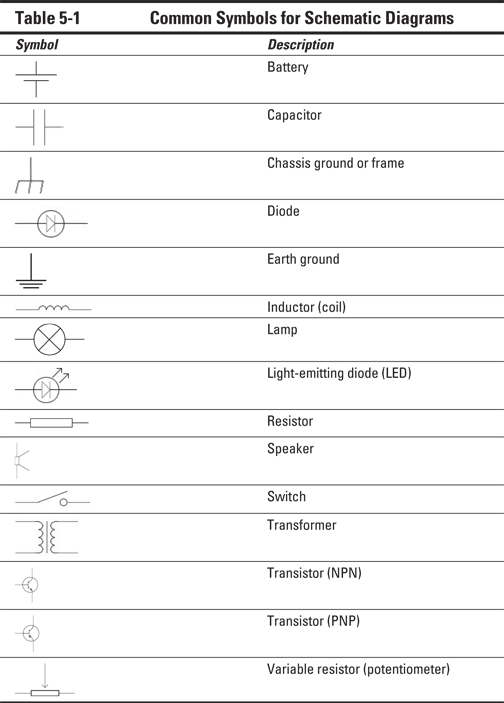
We discuss resistors, capacitors, diodes and transistors in Book II, Chapters 2, 3, 5 and 6, respectively.
Figure 5-3 shows a schematic diagram that includes several of these components. Don’t worry – you don’t need to understand this diagram right now. We just want you to get an idea of what real-world schematic diagrams look like and how to read them.

Figure 5-3: A typical schematic diagram.
As you can see, the circuit in Figure 5-3 contains six components. Working from left to right, they are:
![]() 6 V battery
6 V battery
![]() NPN transistor
NPN transistor
![]() Resistor
Resistor
![]() Capacitor
Capacitor
![]() PNP transistor (at the top right)
PNP transistor (at the top right)
![]() Light-emitting diode (at the bottom right)
Light-emitting diode (at the bottom right)
Throughout the course of this book, we use these and other symbols in the schematic diagrams that describe the circuits. Whenever we use a symbol for the first time, we explain what it is and how it works.
Representing integrated circuits in a schematic diagram
One important symbol that isn’t shown in Table 5-1 is the one for integrated circuits (ICs, which you can read more about in Book III). ICs are small assemblies that usually have multiple leads, called pins, which connect to various parts of the circuit contained within the assembly. Some ICs have as few as six or eight pins; others have dozens or even hundreds. These pins are numbered, beginning with pin 1.
 Each pin in an IC has a distinct purpose, and so connecting to the correct pins in your circuit is vital to the circuit’s proper operation. If you connect to the wrong pins, your circuit doesn’t work and you may damage the IC.
The most common way to depict an IC in a schematic diagram is as a simple rectangle with leads coming out of it to represent the various pins.
The arrangement of the pins in the schematic diagram doesn’t necessarily correspond to the physical arrangement of pins on the IC itself. Instead, the pins are positioned to provide the simplest circuit paths in the diagram. The pins in the diagram are numbered to indicate the correct pin to use.
For example, Figure 5-4 shows a schematic diagram that uses a popular IC (called a 555 timer IC) to make an LED flash. The 555 has eight pins, and you can see that the schematic calls for connections on all eight. However, the pins in the diagram are arranged in a manner that simplifies the connections you need to make to the pins. In an actual 555 IC, the pins are arranged in numerical order on either side of the IC, with pins 1 through 4 on one side and pins 5 through 8 on the other side.
You can discover the details of the operation of this circuit in Book III, Chapter 2. We include it here only so that you can see how ICs are depicted in a schematic diagram.

Figure 5-4: A circuit that uses an integrated circuit.
Simplifying Ground and Power Connections
In many electronic circuits, the distribution of voltage connections is one of the most complicated aspects of the circuit. For example, about half of the connections in the schematic diagram shown in the earlier Figure 5-3 are used to connect the resistor, transistors and LED to the positive or negative terminal of the battery.
More complicated circuits can have hundreds of power connections. If all the lines representing those connections had to be drawn to the positive or negative side of the battery symbol, schematic diagrams would quickly be overwhelmed by the power connections.
Most circuits have a common path by which current returns to its source. In the case of Figure 5-3, the conductor at the very bottom of the diagram collects current from the LED and the resistor and returns it to the battery. This conductor is necessary to complete the circuit so that current can flow in a complete loop from the battery through the various components and then back to the battery.
This common return path is often called the ground, and can be replaced by the earth ground symbol shown earlier in Table 5-1. You may also see the chassis ground symbol used to represent common ground.
Figure 5-5 shows a schematic diagram that uses ground symbols instead of a line to show the path by which current returns to the battery. (The circuit in Figure 5-5 is identical to the one shown in the earlier Figure 5-3.)

Figure 5-5: A schematic diagram that uses a common ground to complete the circuit.
In addition to a common ground path, most circuits also have a common voltage path. In the case of the circuit shown in Figures 5-3 and 5-5, the common voltage path goes from the battery to the resistor and on to the second transistor. This conductor can be replaced by symbols representing voltage sources that appear wherever voltage is required in a circuit.
The symbol used for a voltage source is an open circle or an arrow. The quantity of voltage is always indicated next to the circle or arrow. When a voltage source symbol is used in a schematic diagram, the symbol for the battery (or other power source if the circuit isn’t powered by a battery) is omitted. Instead, the presence of voltage source symbols implies that voltage is provided by some means, by a battery or some other device such as a solar cell or by a power supply plugged into an electrical outlet.
Figure 5-6 illustrates a schematic diagram for the same circuit shown in Figures 5-3 and 5-5, but with voltage source symbols instead of a battery symbol. As you can see, +6 V is required at two places in the circuit: at the resistor and at the second transistor. This circuit is functionally identical to the circuits in Figures 5-3 and 5-4.

Figure 5-6: A schematic diagram that uses a common ground to complete the circuit, with voltage source symbols.
Although the circuit shown in Figure 5-6 has a positive voltage source and the ground is negative, this isn’t always the case. You can also use the voltage source symbol to refer to negative voltage. In that case, the ground actually carries positive voltage back to the source.
In some cases, a circuit may require positive and negative voltages at different places within the circuit. As we explain in Chapter 2 of this minibook, voltages are always measured with respect to two points in a circuit. Thus, voltages are always relative. For example, the positive pole of an AAA battery is +1.5 V relative to the negative pole. At the same time, the negative pole of the battery is –1.5 V relative to the positive pole.
Now suppose that you connect two AAA batteries end to end. Then, the voltage at the positive terminal of the first battery is +3 V relative to the voltage at the negative terminal of the second battery. But the voltage at the positive pole of the first battery is +1.5 V relative to the point between the batteries, and the voltage at the negative pole of the second battery is –1.5 V relative to the point between the batteries.
Figure 5-7 shows how this arrangement may be drawn in a schematic diagram, with a pair of resistors connected across each battery to the middle point. The diagram on the left shows the batteries and connections to them. The diagram on the right shows the same circuit using ground and voltage source symbols instead.

Figure 5-7: Two equivalent diagrams showing positive and negative voltage sources.
Labelling Components in a Schematic Diagram
A symbol alone isn’t usually enough information to identify an electronic component completely in a schematic diagram. Further information is often included with text that’s placed adjacent to the symbol, as shown in Figure 5-8. This additional information may include the following:
![]() Reference identifier: Each component is usually labelled with a letter that designates the type of component followed by a number that helps identify each component of the same type. For example, if a circuit has four resistors, the resistors are identified as R1, R2, R3 and R4. We show the most commonly used letters in Table 5-2.
Reference identifier: Each component is usually labelled with a letter that designates the type of component followed by a number that helps identify each component of the same type. For example, if a circuit has four resistors, the resistors are identified as R1, R2, R3 and R4. We show the most commonly used letters in Table 5-2.
Table 5-2 Commonly Used Reference Identifiers
|
Letter |
Meaning |
|
R |
Resistor |
|
C |
Capacitor |
|
L |
Inductor |
|
D |
Diode |
|
LED (or D) |
Light-emitting diode |
|
Q |
Transistor |
|
SW |
Switch |
|
IC (or U) |
Integrated circuit |
![]() Value or part number: For components such as resistors and capacitors, the value is given in ohms (for resistors) and microfarads (for capacitors). Thus, a 470 Ω resistor has the number 470 next to it and a 100 μF capacitor has the number 100 next to it. (We discuss the resistor and capacitor measurements and abbreviations in Chapter 3 of this minibook.)
Value or part number: For components such as resistors and capacitors, the value is given in ohms (for resistors) and microfarads (for capacitors). Thus, a 470 Ω resistor has the number 470 next to it and a 100 μF capacitor has the number 100 next to it. (We discuss the resistor and capacitor measurements and abbreviations in Chapter 3 of this minibook.)
The letters K and M are used to denote thousands and millions. For example, a 10,000 Ω resistor is identified as 10K in a schematic.
Components such as diodes, transistors and integrated circuits don’t have values; instead, they have manufacturer part numbers. Thus, you may find a part number such as 1N4001 (for a diode), 2N2222 (for a transistor) or 555 (for an integrated circuit) next to one of these components.
In some cases, the value or part number is omitted from the schematic diagram itself and instead included in a separate parts list that identifies the value or part number of each referenced part that appears in the schematic. In such cases, to find the value or part number of a particular component, you look up the component by its reference identifier in the parts list.

Figure 5-8: A schematic diagram with parts labelled.