Chapter 1
Introducing Integrated Circuits
In This Chapter
![]() Examining integrated circuits
Examining integrated circuits
![]() Protecting against damage
Protecting against damage
![]() Deciphering IC data sheets
Deciphering IC data sheets
![]() Meeting some of the IC family
Meeting some of the IC family
On 25 April 1961, Robert Noyce (an engineer working in Palo Alto, California) received word that a patent application that he’d submitted a year before had been finally approved. The patent was for a new type of device that would soon become known as an integrated circuit. Exactly one month later, on 25 May, President John F. Kennedy announced to the world that the United States was going to the moon.
These two events have a lot in common, because without the integrated circuit NASA probably wouldn’t have been able to pull off Kennedy’s challenge.
In this chapter, you discover the device that put men on the moon and went on to change the world of electronics. You find out how integrated circuits are built, what they can do and why they keep getting smaller and cheaper. We also show you how to incorporate them into your own electronic projects.
Investigating Integrated Circuits
An integrated circuit (also called an IC, silicon chip or just a chip) is an entire electronic circuit – consisting of multiple individual components such as transistors, diodes, resistors, capacitors and the conductive pathways that connect all the components – constructed from a single piece of silicon crystal.
 An IC isn’t a really small circuit board with components mounted on it. In an IC, the individual components are embedded directly into the silicon crystal. Previous circuit fabrication techniques relied on mounting smaller and smaller parts on smaller and smaller circuit boards, but an IC is all one piece.
Instead of just two or three p-n junctions, an IC has thousands of individual p-n junctions. In fact, many modern ICs have millions or even billions of them, all fashioned from a single piece of silicon.
The earliest ICs were simple transistor amplifier circuits with just a few transistors, resistors and capacitors. In fact, they weren’t much more complicated than the circuits you breadboard in Book II, Chapter 6. But today’s ICs are unbelievably complex. At the time we’re writing, the most advanced Intel computer chip had 2.6 billion transistors. That number will probably have grown by the time this book reaches your hands.
Most of the ICs you’re going to use for hobby projects are much more modest, having something in the order of a few dozen transistors. For example, the 555 timer IC, which we describe in Chapter 2 of this minibook, has 20 transistors, 2 diodes and 15 resistors and costs about a pound.
Manufacturing integrated circuits
You don’t have to know how ICs are made to use them, and so you can skip this section if you prefer, but the process is pretty interesting. It’s complex, and varies depending on the type of chip being made, but here’s the typical process:
1. A large, cylindrical piece of silicon crystal is shaved into thin wafers a fraction of a millimetre thick. Each of these wafers are used to create several hundred or thousand finished ICs.
2. A special photoresist solution is deposited on top of the wafer.
3. A mask is applied over the photoresist. The mask is an image of the actual circuit, with some areas transparent to allow light through and others opaque to block the light.
4. The wafer is exposed to intense ultraviolet light, which etches the wafer under the transparent portions of the mask but leaves the areas under the opaque parts of the mask untouched.
5. The mask is removed and any remaining photoresist is cleaned off.
6. The wafer is then exposed to a doping material, which creates n-type and p-type regions in the etched areas of the wafer. (For a review on doping and n-type and p-type semiconductors, take a look at Book II, Chapter 5.)
7. If the circuit design calls for multiple layers stacked on top of one another, the process is repeated for each layer until all the layers are created.
8. The individual ICs are then cut apart and mounted in their final packaging.
The manufacturing process for ICs takes place in a clean room, where workers wear masks and special suits nicknamed ‘bunny suits’ (they only have ears on April Fools’ Day!). This extreme cleanliness is necessary, because even the smallest speck of dust is enormous on a tiny IC.
Each IC goes through a variety of complicated quality tests after the circuit is finished. The process is by no means perfect and so many ICs are discarded.
Packaging integrated circuits
Integrated circuits come in a variety of different package types, but nearly all the ICs you work with in hobby electronics come in a type of package called dual inline package (DIP). Figure 1-1 shows two ICs in DIP packages.
 Yes, we know that the phrase ‘DIP package’ is redundant because the ‘P’ in DIP already stands for ‘package’, but the phrase is commonly used. Some people justify it by claiming that the ‘P’ stands for ‘pin’, removing the redundancy. Like it or not, DIP stands for ‘dual inline package’ and ‘DIP package’ is widely used and considered correct. Get used to it.
The phrase ‘DIP chip’ is also sometimes used to describe ICs in DIP packages. It has a nice ring to it and sounds like something you’d serve at a party.
A DIP package consists of a rectangular plastic or resin case that encloses the IC itself, with two rows of pins on the long sides of the rectangle. The pins on each side jut out a bit from the case and then turn straight down. This arrangement makes the package look like an insect.
The pins on each side of a DIP package are spaced exactly 0.1” (2.54 mm) apart, and the two rows of pins are usually spaced 0.3” (7.62 mm) apart, although some larger DIP packages have wider spacing. In any event, the standard tenth-of-an-inch spacing is perfect for use with solderless breadboards, which have holes spaced at this distance. In fact, the gap that runs down the centre of a solderless breadboard happens to be 0.3” too, which makes it easy to mount DIP chips so that they straddle the gap, as shown in Figure 1-2.

Figure 1-1: Most ICs come in DIP packaging.

Figure 1-2: Solderless breadboards are designed with DIP chips in mind.
Each pin in a DIP package is numbered. Look down on the package from above and you can see an orientation mark, usually a notch, groove or dot. Orient the package so that this mark is on the top and pin 1 is immediately to the left of the mark. The pins are numbered counter-clockwise, working down the left side and then back up the right side until you get to the last pin, which is immediately to the right of the orientation mark (see Figure 1-3).

Figure 1-3: Identifying the pins on a DIP package.
The DIP package in Figure 1-3 is for an eight-pin DIP. Larger DIPs have more pins, but the numbering scheme is always the same: pin 1 is to the left of the orientation mark and the remaining pins are numbered counter-clockwise from it.
Depicting ICs in schematic diagrams
In a schematic diagram, an IC is usually represented simply as a rectangle with circuit connections placed conveniently around the rectangle without regard for the physical positioning of the pins. Each pin connection is labelled, as shown in Figure 1-4.
Notice that the pins in this schematic diagram aren’t in the same order as in the actual DIP package. Thus, when you build this circuit, you have to adjust the wiring layout to accommodate the pin arrangement of the DIP package.
Not all the pins on an IC are always used. Unused pins are usually left out of the schematic diagram. For example, pin 5 isn’t used in the circuit shown in Figure 1-4, and so it’s omitted from the schematic.
Figure 1-4: An IC in a schematic diagram.
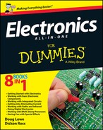
Some ICs contain two or more independent circuits that share a common power supply. For example, the 556 dual timer chip contains two complete 555 timer circuits within a single 14-pin package. When chips like this one are used in a circuit, the schematic diagram may show them separately. For example, Figure 1-5 shows a circuit that calls for a 556 dual timer chip, but each section of the timer is listed separately in the schematic.
Please don’t worry about the details of the circuits in Figures 1-4 and 1-5. We aren’t trying to explain how these circuits work, but only to show you how the ICs are depicted in the schematic diagrams. You can discover more about how these circuits work in Chapter 2 of this minibook.
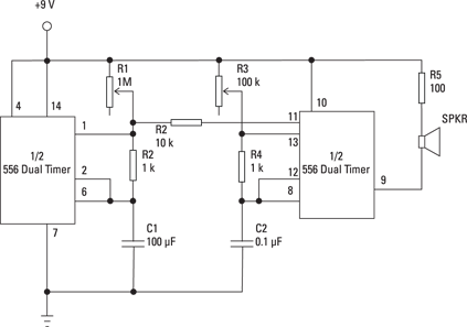
Figure 1-5: Independent sections within a single IC are often shown separately in a schematic diagram.
Powering ICs
In most DIP integrated circuits, two of the pins are used to provide power to the circuit. One of these is designated for positive voltage, typically identified with the symbol VCC. The other is the ground pin. For example, the 555 timer chip (which you can read about in Chapter 3 of this minibook) requires a positive supply voltage between 4.5–15 V at pin 8, and pin 1 is connected to ground.
In the case of ICs that contain two or more separate circuits, the circuits usually share a common power supply. Thus, even though a 556 dual timer chip contains two separate 555 timer circuits, the chip has just one positive voltage pin and one ground pin.
Some ICs call for separate positive and negative supply voltages, not just a positive and a ground connection. You can create a power supply like that using the circuit shown in Figure 1-6.

Figure 1-6: A circuit for providing positive voltage, negative voltage and ground connections.
Avoiding Static and Heat Damage
When you build a circuit board that contains one or more ICs, be careful that you don’t damage the IC when you build your circuit. In particular, watch out for these two possible problems:
![]()
 Heat damage: Some ICs are sensitive to heat, and so take precautions whenever you solder an IC to a circuit board. If possible, attach a crocodile clip to the pin to act as a heat sink that helps to dissipate some of the heat from the IC itself.
You can avoid soldering ICs altogether by using DIP sockets such as the ones shown in Figure 1-7. When you use these sockets, you solder the socket to your circuit board. Then, after the socket is safely soldered in place, you simply insert the IC into the socket.
![]() Static discharge: Many ICs can be damaged by static electricity discharged though your fingers when you handle the chips. Therefore, make sure that you discharge yourself by touching a grounded metal surface before handling an IC. You may also want to use an antistatic wristband when handling ICs.
Static discharge: Many ICs can be damaged by static electricity discharged though your fingers when you handle the chips. Therefore, make sure that you discharge yourself by touching a grounded metal surface before handling an IC. You may also want to use an antistatic wristband when handling ICs.

Figure 1-7: DIP sockets let you avoid soldering delicate ICs.
Reading IC Data Sheets
Before you work with a specific type of IC, download a copy of its data sheet (available from many sources on the Internet, including from the vendors’ websites). Search with the IC part number and ‘data sheet’ or ‘datasheet’. For example, to find a data sheet for a 555 timer chip, search for ‘555 data sheet’.
In addition to basic info such as the manufacturer’s name and the IC part number, the IC data sheet contains loads of useful details such as:
![]() A description of what the circuit does.
A description of what the circuit does.
![]() Detailed pinout descriptions that tell you the purpose of each pin.
Detailed pinout descriptions that tell you the purpose of each pin.
![]() A diagram of the internal circuitry of the chip. For simple circuits, you may get the entire detailed schematic. For more complicated chips, you get a conceptual diagram instead.
A diagram of the internal circuitry of the chip. For simple circuits, you may get the entire detailed schematic. For more complicated chips, you get a conceptual diagram instead.
![]() Detailed electrical specifications, such as maximum voltage you can feed the circuit via the VCC pin or the maximum current loads for output pins.
Detailed electrical specifications, such as maximum voltage you can feed the circuit via the VCC pin or the maximum current loads for output pins.
![]() Operating conditions such as maximum and minimum temperatures.
Operating conditions such as maximum and minimum temperatures.
![]() Charts and graphs that illustrate the circuit’s behaviour for different operating conditions.
Charts and graphs that illustrate the circuit’s behaviour for different operating conditions.
![]() Formulas for calculating operating characteristics of the circuit. For example, if the operation of the circuit depends on an external RC (resistor/capacitor) circuit, you get formulas for calculating how these external components affect the operation of the circuit.
Formulas for calculating operating characteristics of the circuit. For example, if the operation of the circuit depends on an external RC (resistor/capacitor) circuit, you get formulas for calculating how these external components affect the operation of the circuit.
![]() Sample circuit diagrams.
Sample circuit diagrams.
![]() Mechanical descriptions including dimensions.
Mechanical descriptions including dimensions.
Meeting the Family: Popular Integrated Circuits
Thousands of different types of ICs are available, most designed for specific applications. However, many ICs are designed for general-purpose use and can be used in a wide variety of circuits.
In this section, we briefly describe some of the most popular general-purpose ICs. These ICs have been around for decades, but their multipurpose design, wide availability and low cost give them enduring popularity.
555 timer
The 555 timer chip was invented in 1971 but remains one of the most popular ICs in use. By some estimates, more than a billion are made and sold every year.
As its name implies, the 555 is a timer circuit. The timing interval is controlled by an external RC network. In other words, by carefully choosing the values for the resistors and capacitors, you can vary the timing duration.
The 555 can be configured in several different ways. In one configuration (called monostable), it works like an egg timer: you set it and it goes off after a certain period of time elapses. In a different configuration (called astable), the 555 works like a metronome, triggering pulses at regular intervals.
Besides the basic 555 chip, which comes in an 8-pin DIP package, you can also get a 556 dual timer, which contains two independent 555 timers in a single 14-pin DIP package. Many common circuits call for two 555 timers working together, and so the 556 package is very popular.
You can read about the 555 and 556 timers in Chapter 2 of this minibook.
741 and LM324 Op-Amp
An operational amplifier (or op-amp for short) is a special type of amplifier circuit that has many applications throughout electronics. Although many different types of op-amp circuits exist, the 741 and LM324 are the most common.
The 741 is a single op-amp circuit in an eight-pin DIP package. It was first introduced in 1968 and is still one of the most widely used ICs ever made. The 741 is one of those ICs that require positive and negative voltage, as described earlier in the section ‘Powering ICs’.
The LM324 was introduced in 1972 and consists of four separate op-amp circuits in a single 14-pin DIP package. Unlike the 741, the LM324 doesn’t require separate negative and positive voltage supplies.
You can discover more about op-amps in Chapter 3 of this minibook.
78xx voltage regulator
The 78xx is a family of simple voltage regulator ICs. A voltage regulator is a circuit that accepts an input voltage that can vary within a certain range and produces an output voltage that’s a constant value, regardless of fluctuations in the input voltage.
The ‘xx’ represents the actual voltage regulated by the chip. For example, a 7805 produces a 5 V output. The input voltage must be at least a couple of volts over the output voltage, and can be as high as 35 V.
74xx logic family
One of the primary uses for ICs is in digital electronics, and the 74xx is one of the oldest and still most widely used families of digital ICs. The 74xx family includes a variety of chips that provide basic building blocks for digital circuits. Thus, you don’t find complete microprocessors in the 74xx family, but you do find circuits such as logic gates, flip-flops, counters, buffers and so on.
Flip to Book VI, Chapter 3 to read about this useful family of ICs.