
Device families can be used by any MEP discipline to represent the types of components that are crucial to engineering systems but do not necessarily play a major part in the physical model of the systems. Components such as thermostats, switches, and receptacles are all important to how engineering systems are used, yet their size is generally not an issue when it comes to interferences with other model components.
Although devices do not require very detailed modeling, it is useful to have solid geometry that represents the devices in your projects. This will allow you to coordinate their locations in the situations where it is important for collaboration with other disciplines. It may seem unnecessary to model receptacles or switches, but since these types of items are shown in a set of construction documents anyway, you might as well show them correctly in the model for further coordination. With a good library of device families, there is no additional effort to adding model devices as opposed to adding symbols that hold no system information or model intelligence.
Device families can be given connectors that enable them to be included in the engineering systems that you create in your projects. This adds another level of intelligence to the systems and allows you to keep track of things such as circuits and device-component relationships.
Because there is no single standard for devices that is used by all engineers and designers, it is important that you are able to develop the device families that work in the way you design. Of course, it is also important that these components look the way you want them to on your construction documents.
In this chapter, you will learn to
Model device geometry
Use annotations to represent devices
Add parameters and connectors
Creating solid geometry for device families is similar to modeling equipment families only on a smaller scale. The level of detail for devices can be kept very simple to represent the components. In most cases, the geometry does not need to be parametrically controlled, but there are some families where parametric geometry is very useful. Junction boxes are a good example of this. You can create one junction box family with parametric geometry so that multiple types can be created by editing the dimensions of the geometry. This eliminates the need for separate families for each size of junction box.
As with any family you are about to create, you should first decide how the family will be used in your projects. For the most part, device families should be face-hosted families, because it is likely they will be placed in walls, floors, and ceilings. Of course, there are some exceptions such as junction boxes, which you may want to put into the model without a host. The hosting option you choose will determine the family template that will be used. The generic family templates can be used since you can categorize the family once you have started.
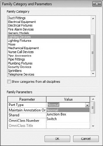
After you have chosen a template to create the family from, click the Family Category And Parameters button to assign the family to a category.
All of the device categories have the same parameters, but the options for the Part Type parameter vary depending on the category. Figure 22.1 shows the available part types for the Lighting Devices category. These are the same options for the Nurse Call and Security Devices categories. The other device categories do not have the Switch option. Using the Switch option allows you to specify the device as the switch for a system in your model.
The Maintain Annotation Orientation parameter is very important for device families that use a nested annotation symbol to represent the object in your model views. This parameter allows the annotation to be displayed regardless of the hosting of the device. This means that the annotation symbol will display whether the device is mounted to a vertical or horizontal surface. If the device is placed on a sloped surface, the annotation will not display.
Select the box for the shared parameter if you want to load your device family into another family and be able to account for the device individually when the host family is used in a project. With this functionality, you could create a family such as a typical systems furniture layout and have the outlets included by nesting them into the furniture family, for example.
The OmniClass parameters are for classifying a family for sharing on websites like Autodesk Seek. If you share a family, it can be identified or filtered based on its classification. You do not need to assign an OmniClass number to your families in order to share them.
With the family category and parameters established, you can begin modeling the geometry of your device family. It is a good idea to establish the category right away, because this will activate certain device-specific parameters, if applicable, and also because once you start working, it is easy to forget until you attempt to use the family in a project. It can be very frustrating to work on a family and load it into a project only to find that it is not available when you click the button to place it in your model.
The amount of solid geometry that you include in a device family depends not only on the object you are creating but also on how it will be used in your projects. If your intent is to only use devices so that their symbols are shown on your plans and you are not concerned with 3D visualization, you can use a simple box. This will at least give you the ability to see the location of the device in section and elevation views for coordination with things such as casework and openings.
Solid geometry is not required in order to place connectors into the family, but it gives you a good reference point for the connectors. The reference planes in the generic family templates define the insertion point of the family. The vertical plane is the center point between the left and right side, while the horizontal plane defines the front and back of the family. The insertion point will be at the intersection of these two planes. You can change the properties of a reference plane so that it will establish the insertion point by editing the Is Reference and Defines Origin parameters.
For face-hosted families, these planes only define the insertion point as it relates to the face of the host extrusion. If you place a device family into a model and attach it to a vertical face, you will need to give it an elevation. A default elevation is assigned in the type properties of the family.

If you have determined that your device family should be parametric, it is best to use reference lines or planes to establish the dimensions that are to be editable. For the most part, the length, width, and depth dimensions should give you enough flexibility to create the various family types within your device family.
When using a reference line or plane to create a dimension, consider how you want the geometry to change upon input of data. Should the geometry grow or shrink in one direction? Does it need to grow equal distances from the center? These types of questions will help you determine the amount and placement of references. The order in which you draw reference planes will determine the direction that a parametric dimension between them will move. This behavior applies only to reference planes. In Figure 22.2, the vertical reference plane on the left was drawn first. When the Length parameter is updated, the reference plane on the right will be the one that moves.

Because the two default reference planes are already in the family when you begin, any reference planes dimensioned to them will move when parameters are updated. You can use the Pin button on the Modify | Reference Planes tab to lock the position of a reference plane. This will keep it from moving when a parametric dimension is updated. Obviously, you cannot pin both reference planes that have a parametric dimension between them; otherwise, you will get an error when the parameter value is changed.
The majority of your device families can be modeled as simple boxes. It is important to create the solid geometry in the proper orientation to how it will be used in your projects. Face-hosted devices should be modeled so that the geometry is inside the host or lying on the surface of the host where applicable. For families that are not parametric, you can simply create the solid geometry as the appropriate size and position it relative to where you want the insertion point.
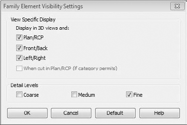
Set the visibility of your device geometry as desired by clicking the Visibility Settings button on the Mode panel when you select a solid form. Even though it is not likely that you will show this geometry in your plan views, it can be helpful to allow the geometry to be visible at some level of detail so that you can determine the exact location of the device when needed. The geometry should be kept visible in Front/Back and Left/Right views so that your devices can be seen in section and elevation. This will allow for coordination with architectural and structural features as well as the ability to edit the device location when working in section or elevation views. Figure 22.3 shows the visibility settings for device geometry that work well for standard model views while allowing for a view of the geometry in Fine detail views. Your results may vary depending on the level of detail used for your plan views at certain scales.
Another option for viewing device family geometry is to create a Yes/No parameter that controls the visibility of the solid forms in the family. The Visible parameter of a solid form can be associated with the Yes/No parameter. This enables you to turn on the geometry when needed for coordination in plan views. However, using this type of visibility control will turn on or turn off the geometry everywhere that it can be seen, so section and elevation views would be affected.
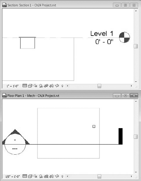
When creating geometry in a face-hosted family, be aware that if you model a solid form so that it is inside the host, the device will not be visible when the family is hosted by a floor unless the view range of the view includes the floor. Figure 22.4 shows a device family hosted by a floor in a project. The device is not visible in the plan view because the bottom of the view range is at the face of the floor. So technically, the device is not within the view range and is therefore not visible.
One way to avoid this scenario is to adjust the view range of your plan views so that the bottom of the view is slightly below the top face of the floor geometry. This could have an adverse effect on the overall look of your floor plan, depending on how the building is designed. Another option is to create the solid geometry in the family so that it protrudes from the host. This may not be a completely accurate representation of the device, but the protrusion can be minimal. Extending past the face of the host just 1/256" (0.1mm) is enough to cause the device to display.

If you are creating a device family for an object that requires a face plate, the plate geometry should be modeled to the surface of the host for a face-hosted family. This eliminates the need to extend the device geometry past the face of the host because the plate geometry will make the family visible when floor hosted. Figure 22.5 shows how adding face plate geometry to the family in the previous example causes it to display properly in the project plan view when hosted by a floor.
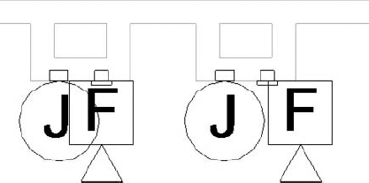
Symbolic lines are useful for adding detail to a device family without adding a lot of complexity to the family. Symbolic lines drawn on the face plate of a device are useful for identifying the device when viewed in section or elevation views. These lines will be visible only in views parallel to the plane in which they are drawn, so they will display in plan views when the device is mounted horizontally only. Vertically hosted devices shown in plan views will not display the symbolic lines; however, the lines will show in section and elevation views. This is useful for interior elevations where devices need to be coordinated with casework or furniture. Can you tell which device is a power receptacle, which is a switch, and which is a telephone outlet in Figure 22.6?

Without symbolic lines to identify the devices, additional information would have to be added to the view for the construction documents. Also, while working in the project, you would have to select the device to see what it is. With symbolic lines added to the families, it is much easier to determine what the devices are in section or elevation views. This can increase coordination of your construction documents and improve productivity during design. Figure 22.7 shows the same devices with symbolic lines added to identify them.

Although the use of symbolic lines is helpful for identifying devices in section and elevation views, these objects are typically represented in plan views by symbols. Annotation families can be added to your device families to represent them in the same manner as you would for a traditional 2D CAD project. Nested annotations can be parametric as well, allowing you to control their orientation and visibility so they can be shown on your construction documents in an appropriate manner.
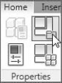
An annotation family is loaded into another family in the same way as loading a family into a project. Click the Load Family button on the Insert tab of the Family Editor to load an annotation family.
For face-hosted families, this is where the Maintain Annotation Orientation parameter is important. When you place an annotation family into your device family, it will only appear in model views that are parallel to the view in which it is placed in the family. With the parameter selected, you can place the annotation in the Ref. Level view of the family, and it will display when the device is hosted vertically. Annotation families cannot be placed into an elevation view when working in the Family Editor.
Once you have loaded an annotation family into your device family, you can place it in the Ref. Level view by dragging it from the Project Browser or by using the Symbol button on the Annotate tab within the Family Editor. While placing the annotation, you can snap to reference planes or reference lines within the device family. The snap point within the annotation is its insertion point defined by the reference planes in the annotation family. You cannot snap line work or geometry to the line work within a nested annotation. Once the annotation is placed, you can use the Move tool to locate the annotation, or you can click and drag it to the desired location.
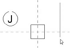
The annotation family that you use in a device family should be located in proper relationship to the geometry of the family so that when the device is placed into a project on a vertical face, the annotation symbol will be aligned with the device host. The insertion point of the annotation family is important to establish a proper relationship to the device geometry as well as the host of the device family. Figure 22.8 shows the location of a junction box annotation family nested into a device family. The insertion point of the annotation is the center of the circle. When the family is used in a project, the annotation does not properly align to the device family host.
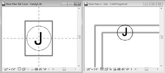
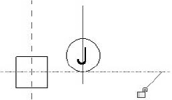
The alignment of the annotation with the vertical reference plane is correct, but regardless of where the annotation is located along that vertical plane, it will display in the project incorrectly. The solution to this problem is to have the insertion point of the annotation at the bottom quadrant of the circle. That way, when the annotation orientation is "maintained," it will display properly, as shown in Figure 22.9.

The orientation of an annotation symbol may not be correct for every instance in your projects. In some cases, the annotation may need to be rotated to display as desired.

You cannot rotate the annotation separately from the device family once the device is placed into a project. If you edit the device family, rotate the annotation, and then load it back into the project, all instances of the device will have a rotated annotation.

Consider using multiple annotations within a device family to allow for displaying a rotated annotation symbol when required. Yes/No parameters can be used to control the visibility of the individual nested annotations, giving you the ability to toggle between annotations when using the device family in a project. Figure 22.10 shows a device family with multiple annotations nested into it.
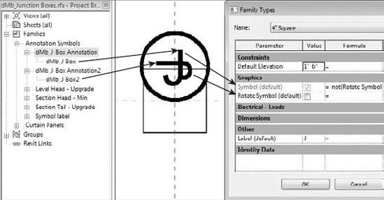
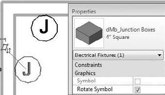
The Symbol parameter controls the visibility of the annotation for normal orientation, and the Rotate Symbol parameter controls the visibility of the rotated annotation. A formula was used so that when working in a project, only one of the boxes can be selected for each instance, preventing accidental display of both annotations. With this type of behavior built into your device families, you can display devices in your projects as desired.
Another method for controlling annotation behavior is to apply an offset parameter so that the annotation symbol can be offset from the actual location of the device. This is useful for situations where two devices are next to each other and their annotation symbols interfere. This can be done directly in the device family by creating a reference plane or line parallel to the plane that defines the left and right sides of the device. A dimension between the plane and line or plane can be associated with an instance parameter that defines the offset distance, as shown in Figure 22.11. The annotation family is aligned and locked to the reference line so that it moves when the dimension is edited.
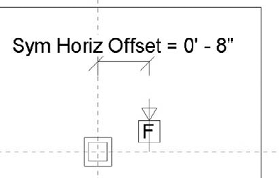
A default of 0'-0" (0mm) can be used for the offset distance to allow for the normal display of the annotation. Using this type of parametric behavior gives you the freedom to locate the annotation symbol in an appropriate location without affecting the device geometry location. You will be able to move the symbol in only one direction, so it may be necessary to rotate the device if the symbol needs to be offset to the other side. Figure 22.12 shows how an offset parameter is used to achieve the desired display of the annotations. The items on the left have interfering symbols because of the locations of the device geometry. The items on the right are displayed properly without affecting the device locations. The device geometry is visible only to show the offset.
You can use this same functionality to create an offset that will pull the annotation away from the device geometry. The offset plane or line can be created directly in the device family only if the family is a nonhosted type. For a face-hosted family, you need to have an offset defined in the annotation family. The parameter that defines the offset can be associated to a parameter in the device family for controlling the offset. See Chapter 18 for how to create an offset within an annotation family.
Having device families that are functional for both your 3D model and your construction documents enables you to be more efficient with your design and project coordination. Now that you have learned about creating a device family with a nested annotation, practice the techniques to make a device family usable in a project by completing the following exercise:
Open the
Ch22_Device Family.rfafile found onwww.wiley.com/go/masteringrevitmep2011.Click the Family Category And Parameters button located on the Properties panel of the Home tab.
In the Family Category And Parameters dialog box, set the category to Electrical Fixtures. Set the Part Type parameter to Junction Box, and select the box for the Maintain Annotation Orientation parameter. Click OK.
Select the extrusion located at the intersection of the reference planes. Click the Visibility Settings button located on the Mode panel of the Modify | Extrusion contextual tab. Remove the check mark from the Front/Back box in the Family Element Visibility Settings dialog box. Remove the check mark from the Coarse and Medium boxes also. Click OK.
Click the Symbol button located on the Detail panel of the Annotate tab. Confirm that the
Ch22_J-BoxAnnotation is shown in the Type Selector, and click to place the annotation symbol in the drawing area, near the extrusion.Click the Reference Line button located on the Datum panel of the Home tab, and draw a vertical reference line to the right of the vertical reference plane.
Click the Align button located on the Modify panel of the Modify tab. Select the vertical reference line drawn in step 6, and then move your mouse pointer over the center of the annotation symbol, highlighting the vertical reference within the annotation. Then click to align the symbol to the reference line. Click the padlock grip to lock the alignment.

With the Align tool still active, click the horizontal reference plane, and then move your mouse pointer near the bottom quadrant of the annotation symbol, highlighting the horizontal reference within the annotation, and click to align the symbol to the reference plane. It is not necessary to lock this alignment.
Click the Aligned button on the Dimension panel of the Annotate tab. Place a dimension between the vertical reference plane and the reference line drawn in step 6. Click the Modify button on the Select panel of the contextual tab.
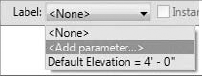
Select the dimension created in step 9. Choose the <Add Parameter ... > option from the Label drop-down on the Options Bar.
Create an instance parameter with the following settings:
Parameter Type: Family
Name: Symbol Offset
Group Parameter Under: Graphics
Click OK to exit the Parameter Properties dialog box.
Click the Family Types button on the Properties panel of the Home tab.
In the Family Types dialog box, set the Symbol Offset parameter value to 0'-0", and click OK.
Save the family to a location that you can access to test its usability in a project.
The device families you create can do more than just indicate device locations on your drawings. Connectors can be added to device families for use with systems. The parameters you add to a device family can hold the engineering data required to connect devices to the appropriate system and account for their effect on the entire system. Adding connectors also allows you to use the wiring tools available in Revit MEP 2011. Revit wire objects that are attached to devices will move and stretch with edits to the device location, reducing the amount of work required to make a simple change.
Using labels in device families seems like the logical solution to provide the information sometimes shown with devices. Although adding text labels to the annotation families that are used in your device families works well, there are some instances where the text needs to be moved for an instance of the device within a project. The best way to have the freedom to move text associated with a device is to create a parameter that holds the value and use a tag in your project that reads that parameter. This places the information directly in your project, not embedded in the device family, allowing you to place the tag wherever you want.
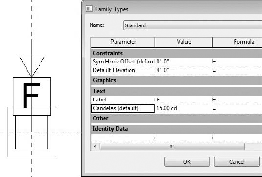
To use a project tag for device labels, you can use one of the coded parameters that exists for the family type. The Description parameter is a good candidate if you are not using it for other information. Keep in mind that this is a type parameter, so whatever value you use will apply to all instances of that type. This can result in having to create unique family types for each unique label. Using a shared parameter allows you to make it an instance parameter that can be a unique value for each instance of the device in your project. If you want to use a custom parameter for the tag, it must be a shared parameter. Figure 22.13 shows that a shared parameter has been added to a device family for its candela rating. There is no label in the device family for this parameter; it is simply there to give a value when the device is tagged in a project.
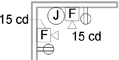
This type of functionality in your device families allows you to place the text associated with the device anywhere in the project view to avoid conflict with other graphics. A tag must be created that reads the parameter used. When creating the tag, be sure to categorize it as a tag for the appropriate type of device. Another benefit of using a tag for a device label is that you can use a leader on the tag when necessary. Figure 22.14 shows how the device with a custom parameter and a tag can be used in a project. The text shown is a Fire Alarm Device tag that was created to read the custom instance parameter called Candelas.
The connectors that you add to device families will most likely be electrical connectors, since these families are the types of building components for controlling systems or power distribution. There are several types of electrical connectors to choose from. The type you add should coincide with the function of the device in your projects.
When you click the Electrical Connector button on the Home tab in the Family Editor, you can choose the connector type from the drop-down on the Options Bar.

The connector can be placed on the face of any 3D geometry that exists in the device family. If you are creating a family without any 3D geometry, you can use the Work Plane placement option for the connector. You can find this option on the Placement panel of the Modify | Place Electrical Connector contextual tab.

An equipment connection and a motor connection are examples of device families that do not have any 3D geometry yet still require a connector for use in the electrical systems defined in your projects. The properties of the connector are what define the system behavior of the device family. Most of the electrical connector system types do not have any parameters for defining electrical behavior. These connectors are simply used for keeping track of connectivity between the devices and their equipment, so their properties are very simple.

The Power-Balanced and Power-Unbalanced system options for a connector contain more properties that are specific to the system behavior. These properties define the electrical characteristics of the device, which then determine the distribution system it can be used with in your projects.
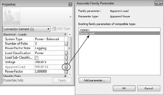
Since you cannot change the properties of a connector without editing the family it resides in, it is best to associate the connector parameters to parameters defined in the device family. This allows you to control the electrical characteristics of the device by editing its properties while working in your projects. A connector parameter can be associated to a family parameter by clicking the small box at the far right of the parameter. This opens a dialog box that lets you select the family parameter to associate the connector parameter to. Only family parameters of the same type will appear in the list. Figure 22.15 shows how the Apparent Load parameter of a connector is associated with a family parameter. Notice that only one parameter is available in the list because it is the only family parameter that is an Apparent Power type.
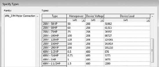
Although the Apparent Load parameter can be an instance parameter, the parameters that you use to define the device's voltage or number of poles should be type parameters. In the case of a motor connection device family where specific loads are used for each voltage, you could use a type parameter for the apparent load. With these settings in place, you can use a type catalog to create the various types of motor connections. Figure 22.16 shows a sample type catalog for a three-phase motor connection device family. The values for the parameters are taken from a code table. This ensures that the proper load values will be used when the devices are connected to systems in a project.
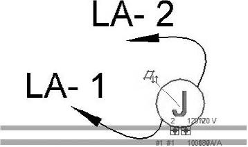
Even though the motor connection family has no 3D geometry, the connector is available when the device is used in a project. Although the location of an electrical connector is not that important in a family that contains 3D geometry, it is very important for a family without geometry. Be sure to locate the connector at the insertion point of the family; otherwise, you can end up with undesired results in your project, as shown in Figure 22.17.
For some device families, you may have the need for multiple connectors. This may be because of different systems within the device or because the device has multiple connection points.

A floor box device family can be created that allows for the connection of all the types of systems within the box. With all the connectors added to the device family, the device can be connected to the appropriate systems when used in a project. Figure 22.18 shows a floor box family with multiple connectors in a project. The systems associated with the connectors can be created for the device in the project.

A junction box is another example of a device family that may require multiple connectors. In this case, the connectors are the same type. Their properties can be associated to the same family parameters or unique ones. Having multiple connectors of the same type within a device family allows you to connect the device to multiple circuits. Figure 22.19 shows how having two connectors in a junction box device family allows the device to be connected to multiple circuits in a project.
Wendy is working on a large office building project. The open floor plan requires systems furniture to be used. She is required to provide a junction box for each group of furniture, but each cubicle within the group needs its own power source. By adding connectors to her junction box family, she is able to show that multiple circuits are provided to each junction box location.
In another area of the building she is using quad receptacles. To limit the load on each circuit, she needs a unique circuit for each pair of outlets within a quad receptacle. She creates a quad receptacle device family that has two connectors. The connector voltages are associated to the device family voltage, and she creates two load parameters, one for each connector.
When using multiple connectors in a device family, it is a good idea to use the Connector Description parameter to identify the connectors. This will help with creating systems when working in a project. When a device has multiple connectors, a dialog box will appear with a list of available connectors when a system is created for the device.
- Model device geometry
The 3D geometry of a device family may not be its most important component, but there are things you can do to make the geometry useful for project coordination and accuracy.
- Master It
Device families are commonly face-hosted because of the way they are used in a project model. Describe why a device family that is hosted by a floor in a project may not display correctly in plan view.
- Use annotations to represent devices
Because of their size and simple shapes, device families are not typically shown on construction documents, but rather a symbol is used to represent the device. Annotation families can be nested into device families for display in project views.
- Master It
The orientation of an annotation family nested into a device family is important for proper display in project views. What is the device family parameter that allows for the display of the annotation in plan and section views? What hosting options in a project allow for this parameter to work?
- Add parameters and connectors
The connectors used in device families provide the engineering characteristics of the device so that it can be incorporated into systems within a project.
- Master It
The parameters of a connector cannot be edited while working in a project file. Describe how you can change the properties of a connector without having to edit the device family.