
1
Combinational Circuit Design
This chapter describes the combinational logic circuits design and their implementation with logic gates, multiplexers, decoders, etc. Combinational circuits are the major block of any digital design or function [1]. So, a detailed overview before the design and analysis of digital circuit with Verilog modules, plays a significant role in hardware optimization to achieve the desired outcomes.
1.1 Logic Gates
Logic gates are very useful when performing a few basic operations in any digital computer system. These logic gates perform many operations in complex circuits and other control systems, e.g., basic operations like AND, OR, and NOT. The functionality of each basic gate as well as the extended version are discussed in this chapter.
AND operation:
It performs the AND operation. The circuit diagram of the N input AND operation is shown in Figure 1.1.

Figure 1.1 Symbol of an AND gate.
The AND gate may have N number of inputs and one output. If the number of inputs are N then N ≥ 2 conditions must be applied for input operation. Digital inputs are applied in terms of A, B, C……N, and the output is Y.
The mathematic equation is given below:

The truth table for an AND gate is provided in Table 1.1
Table 1.1 T. Table of AND gate.
| I/P | O/P | |
|---|---|---|
| A | B | Y |
| 0 | 0 | 0 |
| 0 | 1 | 0 |
| 1 | 0 | 0 |
| 1 | 1 | 1 |
OR operation:
It performs OR operation. The symbol for an OR operation is shown in Figure 1.2.

Figure 1.2 Symbol for an OR gate.
The OR gate may have N number of inputs and one output. If the number of inputs are N then N ≥ 2 conditions must be applied for input operation. Digital inputs are applied in terms of A, B, C……N, and the output is Y.
The mathematic equation is given below:

The truth table for an OR gate is provided in Table 1.2 .
Table 1.2 Truth table of an OR gate.
| I/P | O/P | |
|---|---|---|
| A | B | Y |
| 0 | 0 | 0 |
| 0 | 1 | 1 |
| 1 | 0 | 1 |
| 1 | 1 | 1 |
NOT operation:
This is also called an inverter. The symbol for the NOT gate is shown in Figure 1.3. It has a single input device and it generates an inverted output. Table 1.3 describes the truth table of a NOT gate. The mathematical equation is written as:
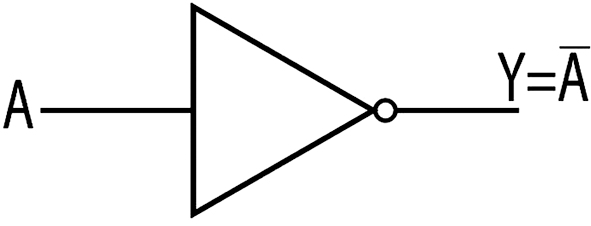
Figure 1.3 Symbol for a NOT gate.

Table 1.3 Truth table of a NOT gate.
| I/P | O/P |
|---|---|
| A | Y |
| 0 | 1 |
| 1 | 0 |
1.1.1 Universal Gate Operation
Universal gates are those in which any logical expression can be realized. The NAND and NOR gates are very popular and are widely used for realization of logical expressions. Therefore, these two NAND and NOR gates are used to implement other gates so these are called universal gates.
NAND operation
This is a universal gate. The operation NOT-AND is known as a NAND operation. It has N number of inputs and one output like other basic gates. However, two inputs and one output NAND gate are shown in Figure 1.4. Table 1.4 provides output values of a NAND gate in terms of inputs. The Boolean equation is given below:

Figure 1.4 Symbol for a NAND gate.

Table 1.4 Truth table of a NAND gate.
| I/P | O/P | |
|---|---|---|
| A | B | Y |
| 0 | 0 | 1 |
| 0 | 1 | 1 |
| 1 | 0 | 1 |
| 1 | 1 | 0 |
NOR operation
This is a universal gate. The operation NOT-OR is known as a NOR operation. It has N number of inputs and one output similar to basic gates. The symbol diagram of two inputs and one output is shown in Figure 1.5. Table 1.5 gives output values of a NOR gate in terms of inputs. The Boolean equation is given below:

Figure 1.5 Symbol for a NOR gate.

Table 1.5 Truth table of a NOR gate.
| I/P | O/P | |
|---|---|---|
| A | B | Y |
| 0 | 0 | 1 |
| 0 | 1 | 0 |
| 1 | 0 | 0 |
| 1 | 1 | 0 |
EX-OR Operation
The operation EX-OR is used in many applications. It has N number of inputs and one output like other basic gates. The symbol diagram of two I/P and one O/P is shown in Figure 1.6. Table 1.6 provides the output values of an EX-OR gate in terms of inputs. Its mathematic equation is given below:

Figure 1.6 Symbol for a NAND gate.

Table 1.6 Truth table of a NAND gate.
| I/P | O/P | |
|---|---|---|
| A | B | Y |
| 0 | 0 | 0 |
| 0 | 1 | 1 |
| 1 | 0 | 1 |
| 1 | 1 | 0 |
1.1.2 Combinational Logic Circuits
This type of circuit depends upon the I/Ps in that particular instant of time. A memory element is not available. A combinational circuit may have a number of sub-systems as shown in Figure 1.7.

Figure 1.7 Diagram of a combinational logic circuit.
There are many ways to design these combinational logic circuits. These include:
- Boolean expression
- Set of statement
- Truth table
These designs are used to design combinational logic circuits. However, a number of methods are also available to simplify Boolean function. These include:
- Algebraic method
- K-map method
- Variable entered method
- Tabulation method
Standard representation for logical functions
Any logical functions can be represented in terms of their logical variables. Logical variables and their functions are in binary form. There are two standard forms generally being used in circuit designing.
- Sum of product (SOP)
- Product of sum (POS)
Apart from the form above, other forms are also available to design circuits. However, these forms are conveniently suitable for the design process. This is discussed in more detail in the next subsection.
1.2 Combinational Logic Circuits Using MSI
This subsection describes the simplification and realization of the combinational logic circuits using gates. These methods are used to integrate complex functions in the form of IC. There are many devices are available such as adders, multiplexers, de-multiplexers, decoders, and multipliers.
1.2.1 Adders
An adder is a combinational logic circuit that performs arithmetic sums of binary numbers and produces corresponding outputs.
Half Adder
This is a basic adder that performs arithmetic sums of two inputs and gives the corresponding output in terms of sum and carry. The diagram of a H. adder is shown in Figure 1.8.

Figure 1.8 Block diagram of a H. adder.
A and B are I/Ps and O/Ps and are the sum and carry of the H. adder. The truth table is given in Table 1.7.
Table 1.7 Truth table of a half adder.
| A | B | SUM | CARRY |
|---|---|---|---|
| 0 | 0 | 0 | 0 |
| 0 | 1 | 1 | 0 |
| 1 | 0 | 1 | 0 |
| 1 | 1 | 0 | 1 |
Mathematical expressions for the H. adder are:

The circuit diagram of the H. adder is shown in Figure 1.9.
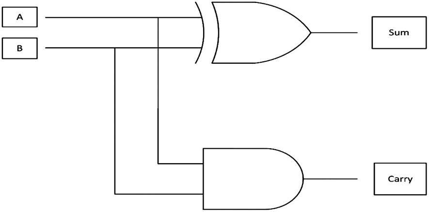
Figure 1.9 Circuit diagram of a half adder.
Full Adder
This performs the arithmetic sum of three inputs and gives the corresponding two outputs in terms of sum and carry. A block diagram of the full adder is shown in Figure 1.10. Table 1.8 provides the truth table of a full adder circuit where output variables (Sum, Cout) are expressed in terms of input values.

Figure 1.10 Block diagram of a full adder.
Table 1.8 Truth table of a full adder.
| A | B | Cin | Sum | Cout |
|---|---|---|---|---|
| 0 | 0 | 0 | 0 | 0 |
| 0 | 0 | 1 | 1 | 0 |
| 0 | 1 | 0 | 1 | 0 |
| 0 | 1 | 1 | 0 | 1 |
| 1 | 0 | 0 | 1 | 0 |
| 1 | 0 | 1 | 0 | 1 |
| 1 | 1 | 0 | 0 | 1 |
| 1 | 1 | 1 | 1 | 1 |
Boolean expressions for the F. adder are:
K-Map for Sum:
| B’Ci’n | B’Cin | BCin | BCin’ | |
|---|---|---|---|---|
| A’ | ➀ | ➀ | ||
| A | ➀ | ➀ |
K-Map for Cout:
| B’Ci’n | B’Cin | BCin | BCin’ | |
|---|---|---|---|---|
| A’ | 1 | |||
| A | 1 | 1 | 1 |
Logic diagram of a full adder


A logical representation of the F. adder is shown in Figure 1.11.

Figure 1.11 Full adder logic block.
Half Subtractor
A half subtractor is a combinational logic circuit that performs the arithmetic difference between two inputs and provides the corresponding output in terms of difference and borrows as shown in Figure 1.12. Table 1.9 provides output variables (Difference, Borrow) of the half subtractor in terms of inputs (A,B).
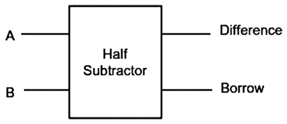
Figure 1.12 Half subtractor.
Table 1.9 Truth table of the H. subtractor.
| A | B | Difference | Borrow |
|---|---|---|---|
| 0 | 0 | 0 | 0 |
| 0 | 1 | 1 | 1 |
| 1 | 0 | 1 | 0 |
| 1 | 1 | 0 | 0 |
Boolean expressions for the H. adder are:

Logic diagram of a H. Subtractor
The logical representation of a H. adder is shown in Figure 1.13.

Figure 1.13 Half subtractor logic block.
Full Subtractor
This performs the arithmetic difference of three inputs and gives corresponding two outputs in terms of Diff. and Borrow. A block diagram of the F. subtractor is shown in Figure 1.14. Table 1.10 provides output variables (Difference, Borrow) of the full subtractor in terms of inputs (A,B).

Figure 1.14 Block diagram of the full subtractor.
Table 1.10 Truth table of the full subtractor.
| A | B | Bin | Diff | Borrow |
|---|---|---|---|---|
| 0 | 0 | 0 | 0 | 0 |
| 0 | 0 | 1 | 1 | 1 |
| 0 | 1 | 0 | 1 | 1 |
| 0 | 1 | 1 | 0 | 1 |
| 1 | 0 | 0 | 1 | 0 |
| 1 | 0 | 1 | 0 | 0 |
| 1 | 1 | 0 | 0 | 0 |
| 1 | 1 | 1 | 1 | 1 |
K-Map for Difference:
| B’Bin’ | B’Bin | BBin | BBin’ | |
| A’ | ||||
| A |
A mathematical equation for the F. subtractor is:

K-Map for Borrow:
| B’Bin’ | B’Bin | BBin | BBin’ | |
| A’ | 1 | 1 | 1 | |
| A | 1 |
The logic diagram of the F. subtractor is shown in Figure 1.15.


Figure 1.15 Full subtractor logic block.
1.2.2 Multiplexers
This is a type of combinational circuit. It has multiple inputs and a single output and its output depends upon the select lines. Select lines control the processing of the multiplexer which means that whatever the input is will be the output depending on select lines. If N select lines then input lines will be 2 N as shown in Figure 1.16.

Figure 1.16 Block diagram of the multiplexer.
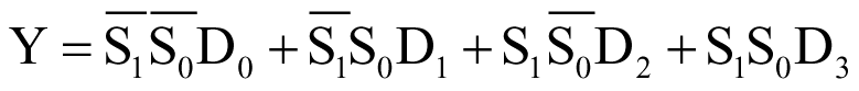
For simplicity of the expression, 4:1 MUX has been explained in the truth table. The truth table for 4:1 MUX is given in Table 1.11.
Table 1.11 Truth table of the 4:1 MUX.
| S1 | S0 | Y(Output) |
|---|---|---|
| 0 | 0 | D0 |
| 0 | 1 | D1 |
| 1 | 0 | D2 |
| 1 | 1 | D3 |
The Boolean expression for Y can be expressed as:
The logic diagram of a multiplexer is shown in Figure 1.17.

Figure 1.17 Logic diagram of the multiplexer.
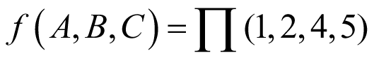
Example:
Implement the expression
Solution:There are four variables; therefore, it needs four select lines for the process. And there are four Minterms which means these inputs are connected with logic 1 and the remaining with logic 0. For this implementation, 8:1 MUX is required. The implementation is shown in Figure 1.18.

Figure 1.18 Implementation of function.
Advantages of multiplexers:
- Logic circuits can be implemented without simplification of the logic expression.
- This reduces the integrated circuit count.
- Logic design can be simplified.
1.2.3 De-multiplexer
A de-multiplexer provides 2N outputs for N select lines and a single input. These controls are used to select which O/P line to route the I/P. For example, a 1 × 4 de-multiplexer has one input and four output lines for two select or control lines, as shown in Figure 1.19. Table 1.12 describes the truth table of the de-multiplexer shown in Figure 1.19.

Figure 1.19 Block diagram of the de-multiplexer.
Table 1.12 Truth table of a 1 × 4 de-multiplexer.
| S1 | S0 | Y3 | Y2 | Y1 | Y0 |
|---|---|---|---|---|---|
| 0 | 0 | 0 | 0 | 0 | In |
| 0 | 1 | 0 | 0 | In | 0 |
| 1 | 0 | 0 | In | 0 | 0 |
| 1 | 1 | In | 0 | 0 | 0 |
With the help of the truth table, the de-multiplexer output can be expressed as:
A logical representation of the de-multiplexer is shown in Figure 1.20.

Figure 1.20 1 × 4 de-multiplexer using logic gates.
1.2.4 Decoders
This is a type of combinational circuit used to decode binary data. There are several decoders such as the BCD to seven-segment decoder, Decimal to BCD decoder etc. Here, the basic decoder 2:4 is being discussed, as shown in Figure 1.21. Table 1.13 shows the truth table of a 2:4 line decoder.

Figure 1.21 Block diagram of a 2 × 4 decoder.
Table 1.13 Truth table of decoder 2 × 4.
| A | B | D0 | D1 | D2 | D3 |
|---|---|---|---|---|---|
| 0 | 0 | 1 | 0 | 0 | 0 |
| 0 | 1 | 0 | 1 | 0 | 0 |
| 1 | 0 | 0 | 0 | 1 | 0 |
| 1 | 1 | 0 | 0 | 0 | 1 |
The truth table of the decoder is given in Table 1.10.
The Boolean function of the output is given below as:

Logic Diagram of Decoder
A logic diagram of the decoder 2 × 4 is shown in Figure 1.22.

Figure 1.22 Logic diagram of a 2 × 4 decoder.
Example:
Implementation of the given functions using a 3:8 decoder.

Solution:
Implementation of the above given function is shown in Figure 1.23.

Figure 1.23 Implementation of functions using the decoder.
1.2.5 Multiplier
A multiplier is a type of combinational circuit which is used to multiply binary numbers. There are several multipliers such as the 2-bit multiplier, 4-bit multiplier, etc.
A block diagram of the 2-bit binary multiplier is shown in Figure 1.24. It will abide by the following sequence in binary multiplication.
| A1 | A0 |
| B1 | B0 |

Figure 1.24 Block diagram of a 2-bit binary multiplier.
………………………
| A1B0 | A0B0 |
| A1B1 | A0B1 |
………………………
| P3 | P2 | P1 | P0 |
Where P0 is the product of two bits only and P1 and P2 will be worked as H. adders, P3 is the carry output. The logic diagram of the 2-bit multiplier is shown in Figure 1.25.
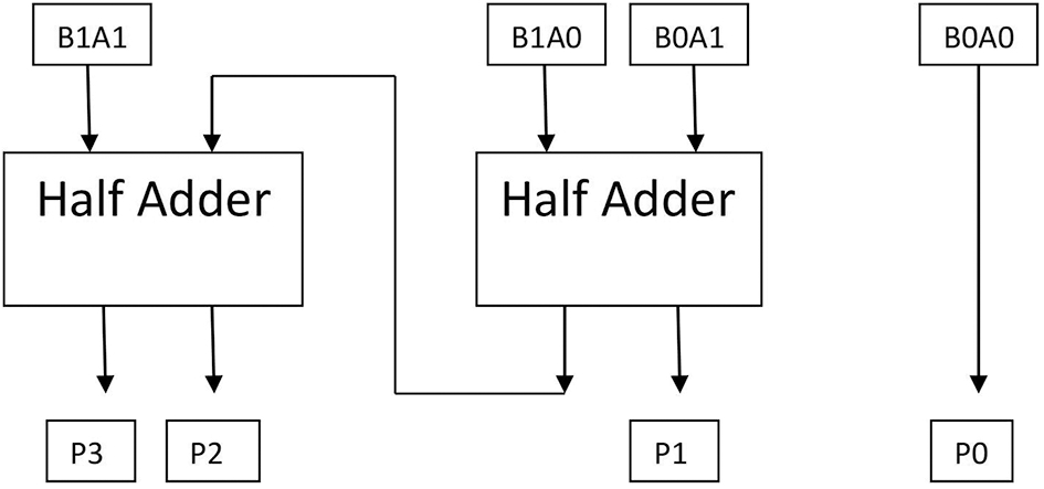
Figure 1.25 Circuit diagram of a 2-bit multiplier.
1.2.6 Comparators
Comparators are the example combinational circuit and can be implemented through a logic gate. Comparators are part of many digital and analog circuits such as ADC to DAC converters, etc. The design of comparators is usually done with the help of a truth table as shown in Table 1.14 for a 2-bit comparator. A 2-bit comparator with input A, B and output Y1(A < B), Y2(A = B) and Y3(A > B) is shown in Figure 1.26.

Figure 1.26 2-bit comparator block.
Table 1.14 Truth table of a 2-bit comparator.
| I/P | O/P | |||||
|---|---|---|---|---|---|---|
| A1 | A0 | B1 | B0 | Y1(A < B) | Y2(A = B) | Y3(A > B) |
| 0 | 0 | 0 | 0 | 0 | 1 | 0 |
| 0 | 0 | 0 | 1 | 1 | 0 | 0 |
| 0 | 0 | 1 | 0 | 1 | 0 | 0 |
| 0 | 0 | 1 | 1 | 1 | 0 | 0 |
| 0 | 1 | 0 | 0 | 0 | 0 | 1 |
| 0 | 1 | 0 | 1 | 0 | 1 | 0 |
| 0 | 1 | 1 | 0 | 1 | 0 | 0 |
| 0 | 1 | 1 | 1 | 1 | 0 | 0 |
| 1 | 0 | 0 | 0 | 0 | 0 | 1 |
| 1 | 0 | 0 | 1 | 0 | 0 | 1 |
| 1 | 0 | 1 | 0 | 0 | 1 | 0 |
| 1 | 0 | 1 | 1 | 1 | 0 | 0 |
| 1 | 1 | 0 | 0 | 0 | 0 | 1 |
| 1 | 1 | 0 | 1 | 0 | 0 | 1 |
| 1 | 1 | 1 | 0 | 0 | 0 | 1 |
| 1 | 1 | 1 | 1 | 0 | 1 | 0 |
We can obtain the out expression for Y1, Y2, and Y3 either by direct implementation with the truth table or by applying K-map reduction techniques.
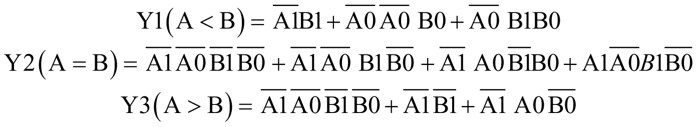
With the above Boolean expressions, a 2-bit comparator can be implemented using logic gates such as AND, OR, and NOT gate.
1.2.7 Code Converters
There is a different format of presentation for digital data like Binary, Octal, Hexadecimal, Gray code, etc. As per the requirement, any one format can be changed into another format with the help of code converters. Several examples would be decimal-to-binary, binary-to-octal or binary-to-hexadecimal, and binary-to-gray and vice versa. The design of code converters is done using logic gates with the help of a truth table (Table 1.15).
Table 1.15 Octal to Binary converter.
| Input in Octal | Output in Binary | |||||||||
|---|---|---|---|---|---|---|---|---|---|---|
| I0 | I1 | I2 | I3 | I4 | I5 | I6 | I7 | B2 | B1 | B0 |
| 1 | 0 | 0 | 0 | 0 | 0 | 0 | 0 | 0 | 0 | 0 |
| 0 | 1 | 0 | 0 | 0 | 0 | 0 | 0 | 0 | 0 | 1 |
| 0 | 0 | 1 | 0 | 0 | 0 | 0 | 0 | 0 | 1 | 0 |
| 0 | 0 | 0 | 1 | 0 | 0 | 0 | 0 | 0 | 1 | 1 |
| 0 | 0 | 0 | 0 | 1 | 0 | 0 | 0 | 1 | 0 | 0 |
| 0 | 0 | 0 | 0 | 0 | 1 | 0 | 0 | 1 | 0 | 1 |
| 0 | 0 | 0 | 0 | 0 | 0 | 1 | 0 | 1 | 1 | 0 |
| 0 | 0 | 0 | 0 | 0 | 0 | 0 | 1 | 1 | 1 | 1 |
Example:
Binary-to-Octal
From Table 1.15, the binary O/P can be derived in terms of I/P as an octal value.

Therefore, octal-to-binary implementation required the OR gate to obtain binary output in terms of octal as input variables.
1.2.8 Decimal to BCD Encoder
This is a type of priority encoder used to convert decimal to BCD number. It takes inputs in the form of numerals between 0 to 9 and gives corresponding BCD output. It works like switches; the response of the 1 or 0 turning them ON or OFF switch mode. Table 1.16 gives output values (BCD) in terms of input values.
Table 1.16 Truth table of a decimal to BCD encoder.
| Input | Output | ||||||||||||
|---|---|---|---|---|---|---|---|---|---|---|---|---|---|
| D9 | D8 | D7 | D6 | D5 | D4 | D3 | D2 | D1 | D0 | Y3 | Y2 | Y1 | Y0 |
| 0 | 0 | 0 | 0 | 0 | 0 | 0 | 0 | 0 | 1 | 0 | 0 | 0 | 0 |
| 0 | 0 | 0 | 0 | 0 | 0 | 0 | 0 | 1 | 0 | 0 | 0 | 0 | 1 |
| 0 | 0 | 0 | 0 | 0 | 0 | 0 | 1 | 0 | 0 | 0 | 0 | 1 | 0 |
| 0 | 0 | 0 | 0 | 0 | 0 | 1 | 0 | 0 | 0 | 0 | 0 | 1 | 1 |
| 0 | 0 | 0 | 0 | 0 | 1 | 0 | 0 | 0 | 0 | 0 | 1 | 0 | 0 |
| 0 | 0 | 0 | 0 | 1 | 0 | 0 | 0 | 0 | 0 | 0 | 1 | 0 | 1 |
| 0 | 0 | 0 | 1 | 0 | 0 | 0 | 0 | 0 | 0 | 0 | 1 | 1 | 0 |
| 0 | 0 | 1 | 0 | 0 | 0 | 0 | 0 | 0 | 0 | 0 | 1 | 0 | 0 |
| 0 | 1 | 0 | 0 | 0 | 0 | 0 | 0 | 0 | 0 | 1 | 0 | 0 | 0 |
| 1 | 0 | 0 | 0 | 0 | 0 | 0 | 0 | 0 | 0 | 1 | 0 | 0 | 1 |
From Table 1.16, the BCD O/P can be represented in terms of I/P as a decimal value.

Therefore, decimal to BCD encoder implementation requires the OR gate to obtain BCD output in terms of decimal as input variables.
Review Questions
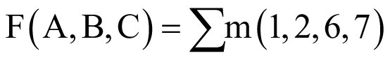
Q1 Design and implement the given function using logic gates at gate level model:

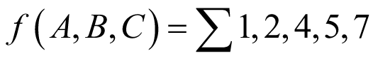
Q2 Implement the following functions using NAND only.

Q3 Implement the following multiple output function using a suitable decoder.

Q4 Implement the following multiple output function using a suitable multiplexer.
Q5 Implement the given function using 4 × 1 multiplexer:

Multiple Choice Questions
Q1 Select the correct representation of given function
- A’B’C + A’BC’ + A’B’C’ + AB’C + ABC
- A’B’C + A’BC’ + AB’C’ + AB’C + ABC
- A’B’C + A’BC’ + AB’C’ + AB’C + ABC’
- A’B’ + A’BC’ + AB’C’ + AB’C + ABC
Q2 Select the correct representation of given function
- A’B’C’ + A’BC + ABC’ + ABC
- A’B’C + A’BC’ + AB’C’ + ABC
- A’B’C + A’BC’ + AB’C’ + ABC
- AB’ + A’BC’ + AB’C’ + ABC
Q3 Select the option which does not match with

- F = a’b’c + a’bc’ + ab’c’ + abc’
- F = a’bc + a’bc’ + ab’c’ + abc’
- Option a and b
Q4 How many 4 × 1 multiplexers are required to implement 16 × 1 multiplexer?
- 4
- 6
- 5
- 6
Q5 The output of a logic gate is 1 when all its input are at logic 0, gate is
- NAND, EXOR
- OR, EXNOR
- AND, EXOR
- NOR, EXNOR
Reference
- [1] Morris, M.M., and Ciletti, M.D. (2018). Digital Design. Upper Saddle River, NJ: Pearson.