
4
Programming Techniques in Verilog I
4.1 Programming Techniques in Verilog I
Verilog HDL is a synthesized tool through which circuit designers can design their desired circuit in their own way. In Verilog, the digital circuit can be described in terms of a network of digital components. Verilog programming has the same C language type syntax. Verilog is used to describe hardware whereas C language is considered software language. In Verilog, the statements are concurrent compared to other languages. In other languages, the statements execute sequentially. The basic building block for writing Verilog code is the module statement. In a module definition, all input as well as output of the desired circuit is defined. Synthesized Verilog codes are mapped to the actual hardware logic gates of the circuits. In this chapter, the gate-level modeling of the circuit is described with the help of different types of circuit.
4.2 Gate-Level Model of Circuits
In gate-level modeling, logic gates used in the circuits are called from the available library of Verilog HDL. In this modeling, the logic gates used have one-to-one relations inside the hardware schematic. The gate-level model is considered as the lowest level of design model.
Example 1: A basic logic circuit at gate level is shown in Figure 4.1.

Figure 4.1 Logic circuit.
Verilog Code:
module Circuit(A,B,F);input A, B;output F;wire W;not (W,B);and (F,A,W);endmodule
Example 2: A logic circuit with AND, OR, and NOT gate is shown in Figure 4.2.

Figure 4.2 Logic circuit.
Verilog Code:
module circuit(A,B,C,X,Y);input A,B,C;output X,Y;wire w;and g1(w,A,B);not g2(Y, C);or g3(X,w,Y);endmodule
4.3 Combinational Circuits
In digital logic design, the circuit where output depends on the combination of present inputs, and does not depend upon previous inputs, is called a combinational circuit. It consists of logic gates, input variables, and output variables.
Gate-level modeling of a combinational circuit
- Adder and Subtractor
- Multiplexer and De-multiplexer
- Decoder and Encoder
- Comparator
4.3.1 Adder and Subtractor
4.3.1.1 Adder
In adder, irrespective of inputs, there are always two outputs in terms of sum and carry. A half adder has two inputs whereas in the case of a full adder, the number of inputs becomes three.
Half adder
A and B are the two inputs defined in the half adder whereas S and C are considered outputs. Figure 4.3 shows the block diagram of a half adder circuit. As there are only two inputs, input combinations are four e.g., 00, 01, 10, 11. All possible four combinations, as well as corresponding outputs, are described in Table 4.1.

Figure 4.3 Block diagram of a half adder.
Table 4.1 Half adder.
| Inputs | Outputs | ||
|---|---|---|---|
| A | B | S | C |
| 0 | 0 | 0 | 0 |
| 0 | 1 | 1 | 0 |
| 1 | 0 | 1 | 0 |
| 1 | 1 | 0 | 1 |
Based on the observations given in Table 4.1, one 2-input XOR gates, along with one 2-input AND gate, are required for implementation of the half adder circuit. Figure 4.4 shows the logic diagram of a half adder circuit. The Boolean expression for a half adder is defined as follows:

Figure 4.4 Logic circuit of half adder.
S = A’B + AB’ = AB and C = AB
Verilog Code:
In Verilog code of the half adder using gate-level modeling, inputs and outputs are defined inside the module HA. Inside the module, two logic gates are called.
module HA(A, B, S, C);input A,B;output S,C;xor X_2(S,A,B);and A_2(C, A,B);endmodule
Half Adder using a NAND gate:
A minimum of five NAND gates are required for a half-adder circuit. The circuit using five NAND gates is described in Figure 4.5.

Figure 4.5 Logic circuit of half adder using a NAND gate.
Verilog Code:
In Verilog code of a half adder using NAND, inputs and outputs are defined inside the module half adder. Inside the module, five NAND gates are called along with three wires.
module HA(A, B, S, C);input A,B;output S,C;wire W1,W2,W3;nand N_1(W1,A,B);nand N_2(W2,A,W1);nand N_3(W3,W1,B);nand N_4(S,W2,W3);nand N_5(C,W1,W1);endmodule
Half Adder using NOR gate:
Implementation of the half adder using NOR gates only requires five minimum gates. The circuit using five NOR gates is shown in Figure 4.6.

Figure 4.6 Logic circuit of half adder using NOR gate.
Verilog Code:
In Verilog code of half adder using NOR, inputs and outputs are defined inside the module half adder. Inside the module, five NOR gates are called along with three wires.
module HA(A, B, S, C);input A,B;output S,C;wire W1,W2,W3;nor N_1(W1,A,A);nor N_2(W2,B,B);nor N_3(W3,A,B);nor N_4(C,W1,W2);nor N_5(S,W3,C);endmodule
Full Adder
In a full-adder circuit, A, B, and C are considered as three inputs whereas S and C are considered as output. As there are only three inputs, the input combinations are eight: 000, 001, 010, 011, 100, 101, 110, 111. All possible four combinations, as well as corresponding outputs, are described in Table 4.2. Figure 4.7 presents a block diagram of a full adder.
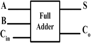
Figure 4.7 Block diagram of a full adder.
Table 4.2 Full adder.
| Inputs | Outputs | |||
|---|---|---|---|---|
| A | B | Cin | S | Co |
| 0 | 0 | 0 | 0 | 0 |
| 0 | 0 | 1 | 1 | 0 |
| 0 | 1 | 0 | 1 | 0 |
| 0 | 1 | 1 | 0 | 1 |
| 1 | 0 | 0 | 1 | 0 |
| 1 | 0 | 1 | 0 | 1 |
| 1 | 1 | 0 | 0 | 1 |
| 1 | 1 | 1 | 1 | 1 |
Based on the observations given in Table 4.2, one 3-input XOR gate, along with three 2-input AND gates, and one 3-input OR gates, are required for implementation of the full-adder circuit. Figure 4.8 presents the logic diagram of a full adder. The expression in terms of three input variables of full adder is defined as follows [1].

Figure 4.8 Logic circuit of a full adder.
S = A’B’Cin + A’BCin’ + AB’Cin’ + ABCin = ABCin
and Co = A’BCin + AB’Cin + ABCin’ + ABCin = AB + BCin + ACin
Verilog Code:
In Verilog code of the full adder using gate-level modeling, inputs and outputs are defined inside the module FA. Inside the module, one XOR gate, three AND gates, as well as one OR gates are used.
module FA(A, B, Cin, S, Co);inputA,B,Cin;outputS,Co;wire W1,W2,W3;xor X_1(S,A,B,Cin);and A_1(W1,A,B);and A_2(W2,A,Cin);and A_3(W3,B,Cin);or O_1(Co,W1,W2,W3);endmodule
4.3.1.2 Subtractor
In subtractor, irrespective of the inputs, there are always two outputs in terms of difference and borrow. In the case of the half subtractor, the number of inputs is two whereas in the case of the full subtractor, the number of inputs becomes three.
Half Subtractor
In the half-subtractor circuit, A and B are two inputs whereas D and B0 are considered as output. As there are only two inputs, the input combinations are four: 00, 01, 10, 11. All possible four combinations, as well as corresponding outputs, are described in Table 4.3. Figure 4.9 presents a half-subtractor block diagram.

Figure 4.9 Block diagram of a half subtractor.
Table 4.3 Half subtractor.
| Inputs | Outputs | |||
|---|---|---|---|---|
| A | B | D | B0 | |
| 0 | 0 | 0 | 0 | |
| 0 | 1 | 1 | 1 | |
| 1 | 0 | 1 | 0 | |
| 1 | 1 | 0 | 0 |
Based on the observations given in Table 4.3, one 2-input XOR gate, along with one 2-input AND gate and one NOT gate, are required for implementation of a half-subtractor circuit. Figure 4.10 presents the logic diagram of a half subtractor. The Boolean expression for the half subtractor is defined as follows [1].

Figure 4.10 Logic circuit of a full subtractor.
D = A’B + AB’ = AB and Bo = A’B
Verilog Code:
In Verilog code of the half subtractor using gate-level modeling, inputs and outputs are defined inside the module HS. Inside the module, three logic gates as well as one wire is called.
module HS(A, B, D, Bo);input A,B;outputD,Bo;wire W;xor X_2(D,A,B);not N_1(W,A)and A_2(Bo, W,B);endmodule
Half Subtractor using NAND gate:
Implementation of the half subtractor using NAND gates only requires a minimum of five NAND gates. The circuit using five NAND gates is described in Figure 4.11.

Figure 4.11 Logic circuit of a half subtractor using a NAND gate.
Verilog Code:
In Verilog code of the half subtractor using NAND, inputs and outputs are defined inside the module HS. Inside the module, five NAND gates are called along with three wires.
module HS(A, B, D, Bo);input A,B;output D,B0;wire W1,W2,W3;nand N_1(W1,A,B);nand N_2(W2,A,W1);nand N_3(W3,W1,B);nand N_4(D,W2,W3);nand N_5(Bo,W3,W3);endmodule
Half Subtractor using NOR gate:
Implementation of the half subtractor using only NOR gates requires a minimum of five gates. The circuit using five NOR gates is described in Figure 4.12.
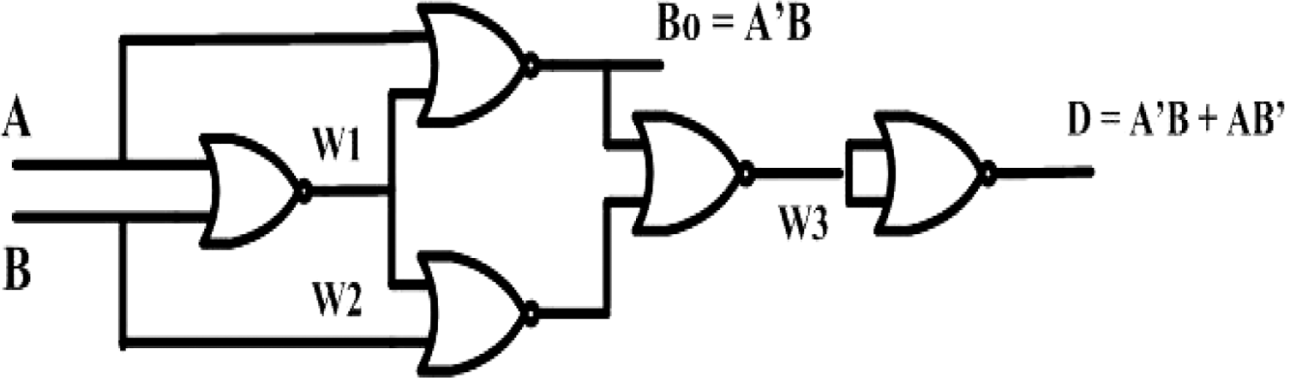
Figure 4.12 Logic circuit of the half subtractor using a NOR gate.
Verilog Code:
In Verilog code of a half subtractor using NOR, inputs and outputs are defined inside the module HS. Inside the module, five NOR gates are called along with three wires [2].
module HS(A, B, D, Bo);input A,B;outputD,Bo;wire W1,W2,W3;nor N_1(W1,A,B);nor N_2(W2,W1,B);nor N_3(Bo,A,W1);nor N_4(W3,Bo,W2);nor N_5(D,W3,W3);endmodule
Full Subtractor
In a full-subtractor circuit A, B, and C are considered as three inputs whereas D and Bo are assumed to be output. As there are only three inputs, the input combinations are eight: 000, 001, 010, 011, 100, 101, 110, 111. All possible four combinations, as well as corresponding outputs, are described in Table 4.4. Figure 4.13 shows the full-subtractor block diagram.

Figure 4.13 Block diagram of a full subtractor.
Table 4.4 Full subtractor.
| Inputs | Outputs | |||
|---|---|---|---|---|
| A | B | C | D | Bo |
| 0 | 0 | 0 | 0 | 0 |
| 0 | 0 | 1 | 1 | 1 |
| 0 | 1 | 0 | 1 | 1 |
| 0 | 1 | 1 | 0 | 1 |
| 1 | 0 | 0 | 1 | 0 |
| 1 | 0 | 1 | 0 | 0 |
| 1 | 1 | 0 | 0 | 0 |
| 1 | 1 | 1 | 1 | 1 |
Based on the observations given in Table 4.4, one 3-input XOR gate, along with three 2-input AND gates, as well as one 3-input OR gate and one NOT gate are required for implementation of a full-subtractor circuit. Figure 4.14 presents the logic diagram of a full subtractor. The Boolean expression for the full subtractor is defined as follows.

Figure 4.14 Logic circuit of a full subtractor.
D = A’B’Cin + A’BCin’ + AB’Cin’ + ABCin = ABCin
and Bo = A’B’Cin + A’BCin’ + A’BCin + ABCin = A’B + BCin + ACin
Verilog Code:
In Verilog code of the full subtractor using gate-level modeling, inputs and outputs are defined inside the module FS. Inside the module, one XOR gate, three AND gates as well as one OR gate are used [2].
module FS(A, B, C, D, Bo);input A,B,C;outputD,Bo;wire W1,W2,W3,W4;xor X_1(D,A,B,C);not n_1(W1,A);and A_1(W2,W1,C);and A_2(W3,W1,B);and A_3(W4,B,C);or O_1(Bo,W2,W3,W4);endmodule
4.3.2 Multiplexer and De-multiplexer
4.3.2.1 Multiplexer
The multiplexer is another combinational circuit which is an important part of digital electronics. Multiplexers are known as data-selector devices, which means they only select one output at a time from the many available inputs based on the select lines [1].
2 × 1 Multiplexer
In a 2 × 1 multiplexer, there are two inputs; one select line and one output line. Based on the select line, the inputs are reflected in terms of output at the output terminal. As only one select line is present in the 2 × 1 multiplexer, there are two options—0 and 1. As shown in Figure 4.15, when 0 is selected at the select line, the I0 is reflected at Y, and when the select line becomes 1, then I1 is considered as output [1].

Figure 4.15 Block diagram of a 2 × 1 multiplexer.
Based on the observations given in Table 4.5, the Boolean expression for a 2 × 1 multiplexer is defined as follows:
Table 4.5 2 × 1 multiplexer.
| Select line | Output |
|---|---|
| S | Y |
| 0 | I0 |
| 1 | I1 |
Y = S' I0 + SI1
Circuit diagram
In the implementation of a 2 × 1 multiplexer, one NOT gate along with two 2-input AND gates, as well as one 2-input OR gates are required [3]. Figure 4.16 presents the logic diagram of a 2 × 1 multiplexer.

Figure 4.16 Logic circuit of a 2 × 1 multiplexer.
Verilog Code
In Verilog code of a 2 × 1 multiplexer using gate-level modeling, inputs and outputs are defined inside the module mux_2x1. Inside the module, one NOT gate, two AND gates as well as one OR gate, along with three wires are used [2].
module mux_2x1(Y,I0,I1,S);input I0,I1,S;output Y;wire W1,W2,W3;not (W1,S);and (W2,I0,W1);and (W3,I1,S);or (Y,W2,W3);endmodule
4 × 1 Multiplexer
In the 4 × 1 multiplexer, there are four inputs, two select lines, and one output line. Based on the select lines, the inputs are reflected in terms of output at the output terminal. As only two select lines are present in a 4 × 1 multiplexer, there are four options: 00, 01, 10, 11. As shown in Figure 4.17, when the select line becomes 00, the I0 is reflected at output port Y, and when the select line becomes 11, then I3 is considered as output [3].

Figure 4.17 Block diagram of a 4 × 1 multiplexer.
Based on the observations given in Table 4.6, the Boolean expression for the 4 × 1 multiplexer is defined as follows:
Table 4.6 4 × 1 multiplexer.
| Select lines | Output | |
|---|---|---|
| S1 | S0 | Y |
| 0 | 0 | I0 |
| 0 | 1 | I1 |
| 1 | 0 | I2 |
| 1 | 1 | I3 |
Y = S1ʹS0ʹI0 + S1ʹS0I1 + S1S0ʹI2 + S1S0I3
Circuit diagram
Two NOT gates, four 3-input AND gates along with one 4-input OR gate are required for the 4 × 1 multiplexer circuit [3] as shown in Figure 4.18.

Figure 4.18 Logic circuit of a 4 × 1 multiplexer.
Verilog Code:
In Verilog code of a 4 × 1 multiplexer using gate-level modeling, inputs and outputs are defined inside the module mux_4x1. Inside the module, two NOT gates, four AND gates, as well as one OR gate, along with six wires are used.
module mux_4x1(Y,I0,I1,I2,I3,S1,S0);input I0,I1,I2,I3,S1,S0;output Y;wire w1,w2,w3,w4,w5,w6;not (w1,S1);not (w2,S0);and (w3,I0,w1,w2);and (w4,I1,w1,S0);and (w5,I2,w2,S1);and (w6,I3,S0,S1);or (Y,w3,w4,w5,w6);endmodule
4.3.2.2 De-multiplexer
The de-multiplexer is a combinational circuit known as a data distributor. In this circuit, a single input is selected through the select line into multiple outputs.
1 × 2 De-multiplexer
In a 1 × 2 de-multiplexer, there is one input, one select line and two output lines. Based on the select line, inputs are reflected in terms of output at the output terminal. As only one select line is present in the 1 × 2 de-multiplexer, there are two options; 0 and 1. As shown in Figure 4.19, when 0 is selected at the select line, D is reflected at output port Y0, and when the select line becomes 1, then input D is reflected at port Y1.

Figure 4.19 Block diagram of 1 × 2 de-multiplexer.
Based on the observations given in Table 4.7, the Boolean expression for a 1 × 2 de-multiplexer is defined as follows:
Table 4.7 1 × 2 de-multiplexer.
| Select line | Input | Outputs | |
|---|---|---|---|
| S | D | Y1 | Y0 |
| 0 | 0 | 0 | 0 |
| 0 | 1 | 0 | 1 |
| 1 | 0 | 0 | 0 |
| 1 | 1 | 1 | 0 |
Y0 = DSʹ
Y1 = DS
Circuit diagram
In the implementation of a 1 × 2 de-multiplexer, one NOT gate along with two 2-input AND gates are required. A 2 × 2 de-multiplexer logic diagram is shown in Figure 4.20.

Figure 4.20 Logic circuit of a 1 × 2 de-multiplexer.
Verilog Code:
In Verilog code of 1 × 2 de-multiplexer using gate-level modeling, inputs and outputs are defined inside the module Dmux_1x2. Inside the module, one NOT gate, as well as two AND gates along with one wire is used.
module Dmux_1x2(D,S,Y0,Y1);input D,S;output Y0,Y1;wire w1;not (w1,s);and (Y0,w1,D);and (Y1,S,D);endmodule
4.3.3 Decoder and Encoder
4.3.3.1 Decoder
The decoder circuit is a combinational circuit having n input gate with 2N number of output gates. If the number of inputs becomes n and the number of output is m then:
m = 2N
2-to-4 Decoder
In the 2-to-4 decoder, there are two input lines as well as four output lines. Based on the selection of input lines, outputs are displayed at the output terminal. As two input lines are present, there are a total of four possibilities: 00, 01, 10, 11. Figure 4.21 shows that when the input lines become 00, the output pin D0 becomes high, and when input lines are 01, 10, 11 then the output pins D1, D2, D3 are high respectively.

Figure 4.21 Block diagram of 2-to-4 decoder.
Based on the observations given in Table 4.8, the Boolean expression of a 2-to-4 decoder is defined as follows:
Table 4.8 2-to-4 decoder
| Inputs | Outputs | ||||
|---|---|---|---|---|---|
| A | B | D0 | D1 | D2 | D3 |
| 0 | 0 | 1 | 0 | 0 | 0 |
| 0 | 1 | 0 | 1 | 0 | 0 |
| 1 | 0 | 0 | 0 | 1 | 0 |
| 1 | 1 | 0 | 0 | 0 | 1 |
D0 = AʹBʹ
D1 = AʹB
D2 = ABʹ
D3 = AB
Circuit diagram
In the implementation of a 2-to-4 decoder, two NOT gates along with four 2-input AND gates are required. Figure 4.22 presents a 2-to-4 line decoder logic circuit.

Figure 4.22 Logic circuit of a 2-to-4 decoder.
Verilog Code :
In Verilog code of a 2-to-4 decoder using gate-level modeling, inputs and outputs are defined inside the module Dec_2to4. Inside the module, two NOT gates, as well as four AND gates along with two wires are used.
module Dec_2to4(A,B,D0,D1,D2,D3);input A,B;output D0,D1,D2,D3;wire w1,w2;not (w1,A);not (w2,B);and (D0,w1,w2);and (D1,w1,B);and (D2,A,w2);and (D3,A,B);endmodule
4.3.3.2 Encoder
The encoder circuit is a combinational circuit with a 2n input gate with n number of output gates. If 4 is the number of inputs, then 2 are the outputs.
4-to-2 Encoder
In a 4-to-2 encoder, there are four inputs and two output lines. Based on the selection of input lines, outputs are displayed at the output terminal. Based on four input lines, possible outputs are 00, 01, 10, 11. Figure 4.23 shows where four input lines W0, W1, W2, and W3 along with two output pins, Y0 and Y1 are present.

Figure 4.23 Block diagram of 4-to-2 encoder.
Based on the observations given in Table 4.9, the Boolean expression for the 4-to-2 encoder is defined as follows:
Table 4.9 4-to-2 encoder.
| Inputs | Outputs | ||||
|---|---|---|---|---|---|
| W3 | W2 | W1 | W0 | Y1 | Y0 |
| 0 | 0 | 0 | 1 | 0 | 0 |
| 0 | 0 | 1 | 0 | 0 | 1 |
| 0 | 1 | 0 | 0 | 1 | 0 |
| 1 | 0 | 0 | 0 | 1 | 1 |
Y1 = W2 + W3
Y0 = W1 + W3
Circuit diagram
In the implementation of a 4-to-2 encoder, two OR gates are required as shown in Figure 4.24.

Figure 4.24 Logic circuit of 4-to-2 encoder.
Verilog Code
In Verilog code of a 4-to-2 encoder using gate-level modeling, inputs and outputs are defined inside the module Enc_4to2. Inside the module, two OR gates are used.
module Enc_4to2(w1,w2,w3,y0,y1);input w1,w2,w3,w4;output y0,y1;or O_1(y0,w1,w3);or O_2(Y1,w2,w3);endmodule
4.3.4 Comparator
The comparator circuit is a combinational circuit which always has three outputs. If two inputs are present in a comparator, the three outputs are A < B, A = B, and A > B. In a 1-bit magnitude comparator, two inputs and three outputs are present.
Based on the observations given in Table 4.10, the Boolean expression for the 1-bit comparator is defined as follows:
Table 4.10 1-bit magnitude comparator.
| Inputs | Outputs | |||
|---|---|---|---|---|
| A | B | A < B | A = B | A > B |
| 0 | 0 | 0 | 1 | 0 |
| 0 | 1 | 1 | 0 | 0 |
| 1 | 0 | 0 | 0 | 1 |
| 1 | 1 | 0 | 1 | 0 |
A < B = > A’B
A > B = > AB’
A = B = > A’B’ + AB
Circuit diagram
In the implementation of a 1-bit comparator circuit, two NOT gates and two AND gates, as well as one XOR gate, are required. This circuit diagram is shown in Figure 4.25.

Figure 4.25 Logic circuit of a 1-bit magnitude comparator.
Verilog Code:
In the Verilog code of a 1-bit magnitude comparator circuit using gate-level modeling, inputs and outputs are defined inside the module Com_1. Inside the module, two NOT gates and two AND gates, as well as one XOR gate, along with two wires are used.
module Com_1(A, B, ALB, AGB, AEB);input A,B;output ALB,AGB,AEB;wire w1,w2;not (w1,A);not (w2,B);and (ALB,w1,B);and (AGB,w2,A);nor (AEB,ALB,AGB);endmodule
Review Questions
Q1 Describe the 4-bit adder circuit and write a Verilog code using gate-level modeling.
Q2 Draw the circuit of an 8 × 1 multiplexer using a 2 × 1 multiplexer and write the Verilog code using gate-level modeling.
Q3 Write a Verilog code to construct a 3-to-8 decoder circuit using gate-level modeling.
Q4 Explain the principle of magnitude comparator and write a Verilog code for a 2-bit magnitude comparator using gate-level modeling.
Q5 Write a Verilog code for a 4-bit adder/subtractor circuit using gate-level modeling.
Multiple Choice Questions
Q1 Verilog programming is case sensitive?
- True
- False
Q2 RTL in Verilog stands for?
- Register transfer logic
- Register transistor logic
- Register transfer level
- All
Q3 How many wires are used in a 4 × 1 multiplexer using gate-level modeling?
- 3
- 4
- 5
- 6
Q4 How many AND gates are called for a 2-to-4 decoder in gate-level modeling?
- 3
- 4
- 6
- 5
Q5 Which keyword is used for equal operator at the output port of a 1-bit magnitude comparator?
- AND
- OR
- NOR
- NAND