

Australian Coast. © Kathryn Watts-Martinez.
Chapter 3 Overview
The sensor is the key to digital capture. This chapter discusses how sensors are constructed and the basics of how they are designed to capture light and color. Within this chapter are considerations of types of metallic oxide semiconductors (MOS), the parts and functions of the sensors, and the architecture used for transferring the signal from the sensor. How the sensors function, how they are manufactured, and the limiting factors of the design of various sensors determine the success of the process.
Types of Sensors
Sensors commonly used in digital capture are metal oxide semiconductors (MOS). This name indicates that the basic elements for construction of the sensors are metal oxides, such as silicon oxide. The term semiconductor refers to the way the electronics function within the sensor. The two primary sensor types used in digital capture are the charge-coupled device (CCD) and the complementary metal oxide semiconductor (CMOS). Both are metal oxide semiconductors. While the CCD is purely a sensor, the CMOS is a computer chip that can have other uses beyond its function as a sensor. Because the CMOS is more versatile and offers economies of manufacture, it tends to be less costly than CCDs for comparably sized sensors.
Metal oxide semiconductor (MOS) A family of semiconductors constructed of metal oxides (such as silicon oxides) that are used to construct digital imaging sensors.
Charge-coupled device (CCD) An electronic device made up of light-sensitive sites arranged to process the output in a linear process. The charges recorded and output from each site are proportional to the light intensity at each site.
Complementary metal oxide semiconductor (CMOS) Computer chips that can be repurposed to act as a sensor. Because they are not specifically a sensor, as in the case of the CCD chip, they can handle many functions of the digital photographic process beyond capturing the light.
Regardless of the type of sensor, the basic unit is the photodiode. The photodiode (site or pixel) (Later) is comprised of layers of silicon, indium, or other metallic compounds that have been etched and assembled to absorb energy. Because visible light is the major source of this energy, the sensors correspond well with human vision. The sensor captures the energy in proportion to the amount of light reaching the sensor’s surface. (Later)
Photodiode The portion of a sensor that actually accepts the light, this is a construction of positive and negative portions (di, meaning two) that allow the light to be captured. These are also called sites.
Site The basic unit of the sensor; it is also called a photosite, photodetector, or pixel.
Electromagnetic spectrum (EMS) Range of energy, from long-wavelength radiowaves to extremely short gamma rays, including human observable light. Digital imaging sensors are capable of capturing the visible light and a portion of the infrared energy.
When considering the photodiode, it is important to understand the scale involved. Typically, the sensitive area of a site used in many digital capture devices is less than 4 μm (1 micrometer = 10 – 6 m). Silver halide crystals are about 1 mm, or about one-quarter the size of common photodiodes. The photodiode has three primary parts: the gate, doped oxide layer, depletion layer, and well. Doping adds a foreign material (a dopant) to the surface that forms positive “holes” that allow the sensor to collect light.
Gate Acts as a control in a digital imaging sensor that allows electrical charge or light energy to have an effect on the operation of the photosite. The gate both allows energy to enter the photodiode and restricts energy flow.
Depletion layer Region between the positive and negative semiconductors of the photodiode. This area is free of electrons or positive “holes.” Without free or exposed charges, this region is considered depleted.
Doping Treating the photosite with an impurity. The dopant causes positive “holes” to be formed that allow the photodiode to collect light.
While the gate can be viewed as the opening for accepting light, it is not always used for entry of the light. In some astronomical sensors, the rear side of the silicon is acid-etched to accept light through that surface. For the sensors used in digital photographic cameras, however, the gate is the access for the light to activate the site. Gates account for only a small amount of the surface or cross section of the sensor. Silicon is often used for the gates, but some are made of more expensive indium tin oxide (ITO) to provide capture across a greater color range. The ability of the sensor to accept light through a gate is increased by doping. Doping of the sensor sandwich allows photons of light with specific energies to be captured. The part of the photodiode that absorbs the light energy is the potential well.
Indium tin oxide (ITO) A material often used in place of silicon to produce the gates of sensors. ITO tends to provide a better color range because it is optically more transparent than polysilicon.
Photons Electromagnetic energy functions in either a wavelength or particle function, and the “photon” is the designation used when the electromagnetic energy is acting as a particle.
Potential well Forms in the silicon base of the sensor when an electrical charge is applied to the photodiode. As the photons of the light are captured, a potential barrier is created that holds the captured energy until it can be discharged.

LSU Theater. © Chipper Hatter.

Figure 3-1 and Figure 3-2 In the charge-coupled device (CCD), both the connection pins and the wires from the surface of the sensor give an indication of the linear electronic function of the chip. With the CMOS, connections around the chip surface and the dark portion that contains active transistors that are not able to acquire light show the more complexity of chip functions of the CMOS
To understand how light is captured, we need to look at the functions and sequencing of the parts and processes used by the sensor. In order to make the process work, the sensor site must be prepared by positively charging all the gates on the sensor. The charging is done for two reasons. First, by applying an equal charge on all gates, a uniform background is created that can be used to measure the changed charge values created by the photons that strike the sensor. The other reason is that photons act as negatively charged particles and, because opposites attract, the positive charge creates the sensitivity required to make an exposure. Because the site is grounded by the potential well, the charge on the gates migrates through the depletion layer to the wells, giving all sites on the sensor the same charges on their wells. Even though the charge has migrated to the well, its charge value is still effective in the capture process. At this point, the site can capture the light energy striking any gate.
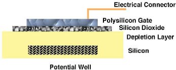
Figure 3-3 Cross section of a photodiode shows the basic parts.
The photons of light are not electrons but they function as negative energy when striking the sensor’s gates. Because the wells now have positive charges, the negative energy created by the light striking the gate is attracted to and captured in the wells. This process continues until the wells reach their maximum capacity. When the negative charge reaches excess capacity at a site, it will migrate to nearby sites. This effect is known as “blooming”; however, most cameras today are manufactured with anti-blooming technology. How the light captured by the photodiodes becomes an image is discussed in Chapter 5.
Blooming When the energy exposing a photosite is greater than can be held in the potential well, it can migrate to nearby sites and is called “blooming.” The effect is of the lightness spreading or streaking from the oversaturated site.
Anti-blooming technology In order to reduce blooming, modern sensors have electrical microcircuits located next to photosites that “drain” excess light-produced charge from the active sites without polluting nearby sites.
The parts of a sensor tell us a great deal about how the light is captured. Manufacturing of the sensors is more involved than might be expected based on their size. Most modern sensors have about 30 manufactured parts and processes. Understanding what goes into the production of the sensor provides insight into the many factors that aid in the functions of the chip. Because sensors are semiconductors, they are often referred to as chips. The common base materials for sensors are metallic wafers, such as those made of silicon. Micro-manufacturing processes such as photoetching, electroplating, coating, and laminating create a sandwich for which the various layers are designed to perform different functions in the operation of the sensor.
Photoetching Digital imaging sensors are constructed on an etched surface. This is accomplished by using photographic resist (protection) to protect parts of the surface from chemical cutting. These relief portions on the sensor’s base material allow other manufacturing processes and electronic connections to be created.
Electroplating A manufacturing process used to create sensors (such as CCD and CMOS) that utilizes electronic energy to deposit a layer of metal to specific locations or pathways within the sensor structure.

Ferris Wheel. © Christopher Gardner.
The most prominent features of sensors are the grid of gates, the electronic connections across the surface, the filters, micro-lenses, (Later) and protective and ultraviolet-reducing covering. The gates create the pattern on the sensor surface. They are regular shapes. Most commonly rectangular gates are used; however, the design and function of the sensor can also call for an octagonal or other polygonal shape. The gates are the only part of the sensor that can record the light. Depending on the shape of the gate and the need for electronics, only part of the surface of the sensor is filled with light-gathering ability. The ratio of the light-sensitive surface to the overall size of the sensor is expressed as a percentage referred to as the fill factor. Depending on the architecture of the sensor and the way it is manufactured, the fill factor will be larger or smaller.
Fill factor The ratio of the lightsensitive surface to the over all size of the sensor.

Figure 3-4 Basic components of sensor.

Lead Sled. © hansenphoto.com.
In color imaging sensors, a filter is located above each gate. The light must be filtered to record color because photodiodes do not differentiate color and only respond to changes in the intensity of the light. The organization of these filters is a product of how the image will be made and the sensor type. The most widely accepted method for color capture utilizes three colors—red, green, and blue (RGB)—to capture the color in the scene. Red, green, and blue represent the primaries of additive light, which means that combining various proportions of these three colors can produce all the colors available in light. Using filters to subtract colors can also create color. This method is called subtractive color mixing, and its primaries are cyan, magenta, and yellow. While a sensor can be manufactured to use subtraction, this type is not common.
In linear arrays filters cover one complete row of the sensor. The linear array has a row of gates covered by a red filter, a row covered by a green filter, and a row covered by a blue filter; thus, this type of array is referred to as a trilinear array. These arrays are used in scanners and scanning camera backs.
Arrays Arrangements of capture or memory elements in one or more planes.
For camera systems that capture images instantaneously, a pattern of filters must be in place to gather all colors simultaneously. Such a pattern is known as the mosaic or filter matrix (also called a Bayer array). This matrix is made up of rows, columns, or diagonals of alternating colors. The pattern of the matrix is R—G—R—G alternating with G—B—G—B. In this way, the pattern has green alternating in perpendicular directions. There are two basic reasons for using a pattern in which green is predominant. Most important is that green light is in the center of the optic sensitivity of the sensor and is most visible to humans. Because detail is more important in image formation than color information and green will record more detail than red or blue, this arrangement of the matrix ensures that the majority of the filters is green. Filters used in the construction of sensors are not pure and will “leak” or cross over small amounts of other colors beyond those in their chromic make-up. This allows crossover through the green filter meaning that energies from the red and blue spectral areas will affect the green sites on the sensor. The second reason for having more green filters than red or blue is that blue is the noisiest channel and restricting its use produces a cleaner image.
Mosaic or filter matrix A pattern of filters used to gather all colors simultaneously in a color sensor.
Bayer array A type of filter matrix used in color imaging for many image sensors. The pattern is alternating rows of filters ordered red–green–red–green and green–blue–green–blue. These filters are arranged so that a green site is never next to another green site.
Another way to capture the color is via the Foveon X3® chip. This sensor uses a natural attribute of silicon to separate the colors. Depending on wavelength, a color will penetrate to varying depths into silicon, similar to what occurs with color film. This factor, along with the stacking of three layers of sites, allows the sensor to capture the light’s color at each stack of photoreceptors. While theoretically there should be no crossover, there is some absorption of colors as the different wavelengths travel through succeeding sensitivity layers.

Figure 3-5 Arrangement of filters for photocells for a matrix or Bayer array.
Sensors are also manufactured that do not have color capture filters or do not acquire color. These cameras are designed to produce monochromatic, black and white images or are used with tricolor photography. Using a monochromatic sensor to produce tricolor photography, filters are placed in the light path to the sensor to make three sequential images—one using red filtration, one using green, and one using blue. A modification of the tricolor photographic process is the three-chip camera, which uses three non-filtered sensors that are positioned to be exposed by light that has been separated into its red, green, or blue spectral portions.

Figure 3-6 and Figure 3-7 The Foveon X3® chip stacks photodiodes to capture all light at a single location. The sensitive areas vary as shown in the colorized patent drawing.
In the most common sensors, micro-lenses are often situated above the filters. These lenses are not used to focus the light but instead concentrate the light as it travels through the filter. Concentrating the light means that the light over those parts of the sensor that are not sensitive is not lost. Just as there is a filter for every site, there is also a micro-lens for each site. “After-processing” of the material that etches the surface of a sensor is often used to create the micro-lenses. In order to etch the surface of the sensor, a material is applied to the parts of the sensor’s surface that will resist the etching. The “resist” will not allow etching on areas where it has been applied. Thus the etching action of the acids does not cut into the surface below the resist, leaving an engraved surface that forms the underlying structure of the sensor. When the etching is completed, the sensor is heated. The heat melts the resist material, forming it into a micro-lens.
Micro-lenses Part of an image sensor above the filters that are used to concentrate light through the filter.
Depending on the sensor, there may also be a glass over the sensor. This provides two benefits. First, the glass provides protection for the micro-manufactured parts, and, second, the glass is often coated with an infrared rejection filter or a “hot mirror” to reduce the sensitivity to reflected infrared wavelengths.
Hot mirror Filter used to block infrared light from the sensor that work by reflecting the nonvisible wavelengths and allowing visible light to pass through.
Many digital sensors are black on the perimeter to block light to photodiodes on the edges. This sets the lowest level of signal strength or dark current reading. While this does not necessarily correspond to black in the captured image, it becomes the base value for exposure.
The basic building block for digital images is the pixel. While there are not actually pixels on the surface of a sensor, people often ask how many pixels the sensor has. While the term pixel is inaccurately used in this case, it has become the industry method of describing the number of active sites on the chip. Both chip size and gate size vary, and both figure into the number. Many sensors have gates as small as 3.4 mm. As mentioned above, because other parts of the functional electronics use the surface of a chip, the number is not just the math of dividing the surface into the gate sizes. Sensors are designed to meet the needs of specific capture devices. For a small cell-phone camera, the sensor might have slightly more than 300,000 sites, while a high-end digital camera might require 6 million or more sites.
Pixel Smallest part or building block of a digital image. The name is derived from the words “picture” (pix) and “element” (el). Pixels are used to refer to both the individual parts of the image and the number of photosites on a sensor.
While defining the number of sites on a chip allows for comparisons between sensors, the physical size of the active sensor surface allows other comparisons of the optical functions of systems. Early in the development of sensors, impurity of the silicon caused problems for larger sensors, but, with improvements, the sensors have become effectively the same size as a roll of film. Today, both CMOS and CCDs are manufactured at sizes larger than a roll of 35-mm film, which has an impact on the number of sites that can be placed on the sensor’s surface and the demands made on the optics. More of these issues are discussed in Chapter 4 dealing with lenses.
Several architectures are used in the processing of signals for sensors. The architecture reflects the way the chip is configured and constructed to move its captured light from the potential wells to image processing. The architecture allows for speedier handling and transfer from the active sensor areas. The transfer can be organized as a linear function or through three potential transferring methods. All the transfer processes use sites or a duplicate array protected from exposure to light and will not be affected by successive exposure. Because the sites or array are not exposed to the light, the charge can be moved from the active photodiodes or active array.
Transfer Refers to a type of architecture used in the processing of digital images on the sensor. The transfer moves the collected energy rapidly. Transfer types include frame, interline, and frame interline.
With frame transfer architecture, the entire frame is rapidly moved to an adjacent fully protected array. Another architecture shifts the captured energy to sites that will not accept light and are parallel to the active sensor sites. This is known as interline transfer. When the two methods are used together, the procedure is referred to as frame interline transfer.

Olympic Jump 6. © Anacleto Rapping—Los Angeles Times.
As we close this chapter, let us compare the CCD and CMOS sensors. Depending on the way we look at the different sensor types, we will see various advantages or benefits. While both sensors will give good results, there are reasons we might wish to select one or the other sensor type. When discussing image quality and color, the CCD gives better results, and most professionals find that they prefer the quality from the CCD compared to the CMOS. Part of this is because the CCD has higher photodiode sensitivity, which produces a cleaner signal with a better signal-to-noise ratio. However, there are also advantages to using CMOS. Because the CMOS is a repurposed computer chip, it can perform many non-imaging functions that must be handled with other circuitry for a CCD. Because the CMOS is used in other computer applications, a greater number of them is manufactured, thus lowering the price. The enhanced computing power of the CMOS offers faster readout of the captured signal. The CMOS is more energy efficient than a CCD and currently can be manufactured with larger surface areas; however, even with recent improvements, the CMOS tends to have a higher noise level because it is more electronically active (the issue of noise is discussed in Chapter 5).
Noise Unwanted electronic information. Noise is common to all electronic equipment and shows up in a digital image as lighter pixels in otherwise dark-toned areas.
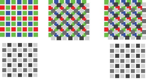
Figure 3-8 Frame transfer and interline transfer interline frame.
Summary
- The two major sensors used in digital cameras are the charge-coupled device (CCD) and the complementary metal oxide semiconductor (CMOS).
- Photodiodes are the active light receptors on a sensor.
- The sensor has many other manufactured parts in addition to the photodiodes.
- Both the construction and structure of sensors are concerned with the capture of color. Two area array structures are used: the Bayer array of filters and the Foveon X3®.
- The structure of the sensors allows the captured charges from the active sites to be moved through various sensor architectures.
Glossary of Terms
Anti-blooming technology In order to reduce blooming, modern sensors have electrical microcircuits located next to photosites that “drain” excess light-produced charge from the active sites without polluting nearby sites.
Arrays Arrangements of capture or memory elements in one or more planes.
Bayer array A type of filter matrix used in color imaging for many image sensors. The pattern is alternating rows of filters ordered red–green–red–green and green–blue–green–blue. These filters are arranged so that a green site is never next to another green site.
Blooming When the energy exposing a photosite is greater than can be held in the potential well, it can migrate to nearby sites and is called “blooming.” The effect is of the lightness spreading or streaking from the oversaturated site.
Charge-coupled device (CCD) An electronic device made up of light-sensitive sites arranged to process the output in a linear process. The charges recorded and output from each site are proportional to the light intensity at each site.
Complementary metal oxide semiconductor (CMOS) Computer chips that can be repurposed to act as a sensor. Because they are not specifically a sensor, as in the case of the CCD chip, they can handle many functions of the digital photographic process beyond capturing the light.
Depletion layer Region between the positive and negative semiconductors of the photodiode. This area is free of electrons or positive “holes.” Without free or exposed charges, this region is considered depleted.
Doping Treating the photosite with an impurity. The dopant causes positive “holes” to be formed that allow the photodiode to collect light.
Electromagnetic spectrum (EMS) Range of energy, from long-wavelength radiowaves to extremely short gamma rays, including human observable light. Digital imaging sensors are capable of capturing the visible light and a portion of the infrared energy.
Electroplating A manufacturing process used to create sensors (such as CCD and CMOS) that utilizes electronic energy to deposit a layer of metal to specific locations or pathways within the sensor structure.
Fill factor The ratio of the light-sensitive surface to the overall size of the sensor.
Gate Acts as a control in a digital imaging sensor that allows electrical charge or light energy to have an effect on the operation of the photosite. The gate both allows energy to enter the photodiode and restricts energy flow.
Hot mirror Filter used to block infrared light from the sensor that works by reflecting the nonvisible wavelengths and allowing visible light to pass through.
Indium tin oxide (ITO) A material often used in place of silicon to produce the gates of sensors. ITO tends to provide a better color range because it is optically more transparent than polysilicon.
Metal oxide semiconductor (MOS) A family of semiconductors constructed of metal oxides (such as silicon oxides) that are used to construct digital imaging sensors.
Micro-lenses Part of an image sensor above the filters that are used to concentrate light through the filter.
Mosaic or filter matrix A pattern of filters used to gather all colors simultaneously in a color sensor.
Noise Unwanted electronic information. Noise is common to all electronic equipment and shows up in a digital image as lighter pixels in otherwise dark-toned areas.
Photodiode The portion of a sensor that actually accepts the light, this is a construction of positive and negative portions (di, meaning two) that allow the light to be captured. These are also called sites.
Photoetching Digital imaging sensors are constructed on an etched surface. This is accomplished by using photographic resist (protection) to protect parts of the surface from chemical cutting. These relief portions on the sensor’s base material allow other manufacturing processes and electronic connections to be created.
Photons Electromagnetic energy functions in either a wavelength or particle function, and the “photon” is the designation used when the electromagnetic energy is acting as a particle.
Pixel Smallest part or building block of a digital image. The name is derived from the words “picture” (pix) and “element” (el). Pixels are used to refer to both the individual parts of the image and the number of photosites on a sensor.
Potential well Forms in the silicon base of the sensor when an electrical charge is applied to the photodiode. As the photons of the light are captured, a potential barrier is created that holds the captured energy until it can be discharged.
Site The basic unit of the sensor; it is also called a photosite, photodetector, or pixel.
Transfer Refers to a type of architecture used in the processing of digital images on the sensor. The transfer moves the collected energy rapidly. Transfer types include frame, interline, and frame interline.