
8
What’s Next: Challenges Ahead
8.1 INTRODUCTION
With rapid advances in transistor density, it is time to look ahead to the future. One extreme is the completely autonomous system-on-chip (ASOC): a convergence of RFID (radio-frequency identification) technology with SOC technology coupled with transducers, sensor controllers, and battery, all on the same die. The major architectural implication is design for extremely low power (down to 1 µW or less) and a strict energy budget. This requires rethinking of clocking, memory organization, and processor organization. The use of deposited thin film batteries, extremely efficient radio frequency (RF) communications, digital sensors, and microelectromechanical systems (MEMS) completes the ASOC plan. Short of this extreme, there are many system configurations providing various trade-offs across power, RF, and speed budgets.
Throughout this text, it is clear that design time and cost are the major SOC limitations now and even more so in the future. One way to address these limitations is to develop a design process in which components can optimize and verify themselves to improve efficiency, reuse, and correctness, the three design challenges identified by the International Technology Roadmap for Semiconductors. Self-optimization and self-verification before and after design deployment are key to future SOC design.
This chapter has two parts. Part I covers the future system: ASOC. Part II covers the future design process: self-optimization and self-verification. There are various challenges which, if met, would enable the opportunities outlined in this chapter. We highlight some of these challenges in the text.
I. THE FUTURE SYSTEM: AUTONOMOUS SYSTEM-ON-CHIP
8.2 OVERVIEW
SOC technology represents an expanding part of the microprocessor marketplace; growing at 20% per annum rate, there’s much more to come [134].
The typical SOC consists of multiple heterogeneous processors and controllers, and several types of memory (read-only memory [ROM], cache, and embedded dynamic random access memory [eDRAM]. The various processors are oriented toward one or more types of media processing. Typical applications include cell phones, digital cameras, MP3 players, and various gaming devices.
Another fast-growing chip marketplace is autonomous chips (ACs). These have little processing power or memory, but have RF communications and some type of self-contained power source or power management. The more elaborate ACs also contain or are coupled with some types of sensors. The simple versions include RFID chips [205], smart cards, and chip-implanted credit cards.
The simplest AC is the passively powered RFID. The chip simply reflects the source RF carrier and modulates it (using carrier power) to indicate its ID. More complex examples include the patient monitoring alarm [31] and the Smart Dust research program [63, 181] of the 1990s. Both of these used battery-powered RF to broadcast an ID on a detected sensor input.
The various Smart Cards and Money Cards include VISA cards and Hong Kong’s Octopus Card. All (except those that require contact) use a form of RFID. The simplest cards are passive without on-card writeable memory. Records are updated centrally. Implementation is frequently based on Java Card [234]. Based on the extraordinary interest, there are a series of contactless identification cards (RFID) standards:
- ISO 10536 close coupling cards (0–1 cm),
- ISO 14443 proximity coupling cards (0–10 cm),
- ISO 15693 vicinity coupling (0–1 m).
The future autonomous SOC or ASOC is the combination of the SOC with the AC technology (Table 8.1). While conceptually simple, the engineering details are formidable as it involves rethinking the whole of processor architecture and implementation to optimize designs for very low power operation—in the submicrowatt region.
TABLE 8.1 Some ASOC Examples
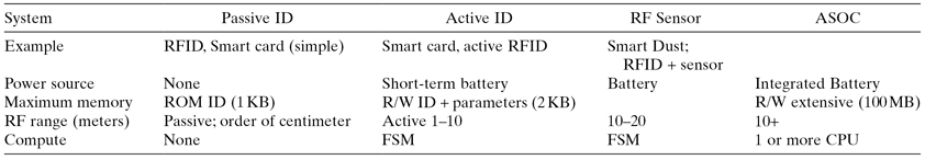
FSM represents a simple finite state machine or microcontroller; R/W: Read/Write memory.
The motivation for ASOC follows the Smart Dust project [63], which started in the early 1990s and pioneered significant work in the sensor and RF areas. That project targeted sensor plus RF integrated into a form factor of the order of 1 mm3 called motes. As a power source it relied on AA type batteries. That project was targeted at sensing an “event,” such as a moving object or a thermal signal.
ASOC is an updated extension of that work that places more emphasis on computational ability and memory capacity; as well as fully integrating a power source on die.
A simplified classification of ACs, by their level of sophistication, is:
1. Simple identification of the die itself (as in RFID) with RF response.
2. Identification of a sensor-detected “event” with RF response (as in Smart Dust and many Smart Cards).
3. Detection of an “event” and processing (classification, recognition, analyzing) the event (ASOC) with RF response of the result.
The ability of the ASOC to process data is clearly valuable in reducing the amount of sensor data required to be transmitted. It enables applications (such as supporting planetary exploration) where interactive computational support is impossible; so too with the recognition of a rare bird or other species in remote areas; or swallowing an ASOC “pill” for diagnosis of the gastrointestinal tract. Not all dimensions of ASOC are equally important in all applications. A rare species “listening” post may require little size concern and may have ample battery support. We look at ASOC as a toolkit for the new systems designer, offering the ability to configure systems to respond to an almost endless set of environmental and computational requirements.
In the next few sections we consider the evolution of silicon technology, limits on batteries and energy, architecture implications, communications, sensors, and applications.
8.3 TECHNOLOGY
As we saw in the earlier chapters over the next few years transistor and memory density is expected to increase 10-fold [134] to several billion transistors/cm2. Since a reasonable powerful processor can be realized with a few 100,000 transistors, there are a lot of possibilities for ASOC applications.
This density, however, has a price. Very small devices pose significant performance problems in traditional workstation implementations. Simply the dopant variability (number of dopant atoms needed to create a device) causes variability in delay from device to device. Small structures involve large electric fields causing reliability problems: electromigration in conductors and diaelectric fatigue. These are not significant problems for ASOC at the very low projected power and speed employed.
The main problem for useful ASOC is battery power or stored energy. In dealing with this issue recall two general relationships discussed in Chapter 2, relating silicon area A, algorithmic execution time T, and power consumption P (in these expressions k is a constant):
(8.1)
![]()
This result [247] simply related area (the number of transistors) to the execution time required to complete an operation. The more area (transistors) used, the faster (smaller) the execution time. Recall from chapter 2 the relationship between execution time and power [99].
(8.2)
![]()
It is easy to see that as voltage is decreased power is reduced by the square but speed is reduced linearly. But in transistors the charging current (representing delay) and voltage have a nonlinear relationship. As we saw in Chapter 2, this gives the cubic result:
(8.3)
![]()
So if we want to double the frequency we should expect the design to use eight times more power. While the range of applicability of expression 8.2 is not precise, suppose we use it to project the frequency of a processor design that operates at a microwatt. The best power–performance design of today might consume 1 W and achieve 1 GHz (corresponding perhaps to 1000 million instructions per second [MIPS]); this may be optimistic. Reducing the power by a factor of 106 should reduce frequency by a factor of 100 or 10 MHz. Within the past 2 years a sensor processor has been built that achieves almost 0.5 MIPS/µW [271]. While this is an order of magnitude away from our target of 10 MHz/µW, silicon scaling projections may compensate for the difference.
CHALLENGE
Is the T3P = k rule robust down to microwatts?
We know that this rule seems valid at the usual operating conditions, but how can we scale it to microwatts? What circuits and devices are required?
8.4 POWERING THE ASOC
The key problems in forming robust ASOC are energy and lifetime. Both relate to the power source, that is, the battery. Batteries can be charged once or are rechargeable (with varying recharge cycles). For ASOC purposes, rechargeable batteries use scavenged energy from the environment. The capacity of the battery is usually measured in milliamp-hours; which we convert to joules (watt-seconds) at about 1.5 V. Both capacity and rechargeability depend on size, which we assume is generally consistent with the size and weight of the ASOC die (about 1 cm2 surface area).
In Table 8.2 we list three common battery types: the printed [47, 203] and thin film batteries [67] can be directly integrated into the ASOC die (usually the reverse side); button batteries are external and are less than 1 cm in diameter.
TABLE 8.2 Batteries of ASOC
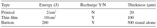
Printed batteries are formed by printing with special inks in a flat surface; thin film batteries are deposited on silicon much as the system die itself.
CHALLENGE
Battery technology that can provide over 100 J in form factor of 1 cm2 × 100 µm that can be deposited on a silicon substrate.
Microbattery technology is emerging as a critical new need for many applications.
Energy may be scavenged from many sources (some are illustrated in Table 8.3); usually the larger the battery format, the more the charge. Much depends on the system environment as to which, if any, scavenging is suitable.
TABLE 8.3 Some Energy-Scavenging Sources [173, 195, 206]
| Source | Charge rate | Comment |
| Solar | 65 (milliwatts per square centimeter) | |
| Ambient light | 2 (milliwatts per square centimeter) | |
| Strain and acoustic | A force (sound) changes alignment of crystal structure, creating voltage | Piezoelectric effect |
| RF | An electric field of 10 V/m yields 16 µW/cm2 of antenna | See Yeatman [266] |
| Temperature difference (Peltier effect) | 40 (microwatts per 5°C difference) | Needs temperature differential |
Assuming ASOC consumption of 1 µW (when active), the operational lifetime between charges is plotted in Figure 8.1. Duty cycle can play an important role in expending the ASOC serviceability. The assumption is that a passive sensor can detect an event and power up the system for analysis.
Figure 8.1 Maximum time between recharge for 1 µW of continuous power consumption.
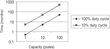
Comparing Figures 8.1 and 8.2, if we can configure the ASOC to use of the order of 1 µW we should be able to incorporate a suitable battery technology especially if we have the ability to scavenge some addition energy.
Figure 8.2 The area–time–power trade-off.

CHALLENGE
Scavenge energy from many more sources with ready implementation technologies.
To date, most attention on energy scavenging has been restricted to light and possibly RF (as in RFID). We need an integrated study of alternatives, especially when the amount scavenged is in microwatts. In the past, such low power recovery was considered useless; with ASOC it becomes useful.
8.5 THE SHAPE OF THE ASOC
The logical pieces of the ASOC die are shown in Figure 8.3. It consists of the power source, sensors(s), main computer and memory, and the communications module. What distinguishes the ASOC from the earlier RFID plus sensor technology is the compute power and memory. It is this facility that enables the system to analyze and distinguish patterns, to synthesize responses before communicating with the external environment.
Figure 8.3 An ASOC die.

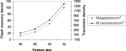
Physically the ASOC is just a silicon die, probably 1 cm2 in surface area. Surface size is dictated by cost, which is determined by defect density. Current technology gives excellent yields for 1 cm2 and smaller die sizes. Much below 1 cm2 costs are limited by testing and handling so this represents the preferred size for most applications. Die thickness is limited by wafer fabrication considerations and is about 600 µm. A thin film battery deposited in the reverse side might add another 50 µm. The resultant ASOC would be 65 mm3 and weigh about 0.2 g. From Figure 8.4 it could have of the order of 1 billion transistors. These transistors would realize the sensors, computer, memory, and RF; the battery is on the reverse side.
Figure 8.4 ITRS [134] projection for transistor density.
8.6 COMPUTER MODULE AND MEMORY
With a power budget of only 1 µW the microarchitecture of the computer is considerably different from the conventional processor:
1. Asynchronous clocking: Data state transitions must be minimized to reduce dynamic power. There may be only one-tenth asynchronous transitions required compared to a clocked system.
2. Use of VLIW: Transistors are plentiful but power is scarce, so the effort is to use any available parallelism to recover performance.
3. Beckett and Goldstein [39] have shown that by careful device design (lowering drive current and managing leakage), it is possible to arrange for overall die power to be a reducing function of die area. This sacrifices maximum operating frequency but the additional area can more than compensate by parallelizing aspects of the architecture.
4. Minimum and simple cache system: The memory and processor are in relatively closer time proximity if the processor is performing an action once every 0.1 µs and the flash memory has access time between 1 and 10 µs. A small instruction cache and explicitly managed data buffers seem most suitable in the context of specified applications.
The flash memory is another essential piece of the system as it has a persistent data image even without power. Current densities (NAND-based flash) give excellent access times, 10 µs, and ASOC capacity of perhaps 16–64 MB.
As the technology is currently configured, Flash is largely incompatible with integrated CMOS technology and seems restricted to off-die implementations. However, there are a number of Flash variants that are specifically designed to be compatible with ordinary SOC technology. SONOS [233] is a nonvolatile example and Z-RAM [91] is a DRAM replacement example. Neither seems to suffer from the conventional Flash rewrite cycle limitations (the order of 100,000 writes).
Even though the Flash memory consumes no power when it is not being used, when it is accessed the power consumption is proportional to the active memory array size; that is, the number of memory cells connected to each bit and word-line (assuming 2-D square structure). In the context of ASOC this implies a memory partitioned into smaller units, which may be most effective from both a power and access time basis.
8.7 RF OR LIGHT COMMUNICATIONS
One of the great challenges of ASOC is communications. There are two obvious approaches: laser and RF communications.
CHALLENGE
Extremely low power processors that achieve perhaps 1/100 of the performance of a conventional processor with microwatt power.
This requires a rethinking of processor design issues from the device level (absolutely minimum static power) to new circuit technology (subthreshold or adiabatic circuits); new clocking; and finally, a completely new look at architectures.
8.7.1 Lasers
Integrating laser with silicon is an emerging technology. A recent development [85] uses an Indium Phosphide laser with silicon waveguide bonded directly to a silicon chip. Using lasers for optical free-space communications has possibilities and difficulties.
Optical sensors are quite responsive [136]; reception of 1 µW supports about 100 MHz data rates (Figure 8.5). The difficulty is that reception is subject to ambient light (noise). In general the signal must be 10 times greater than the noise. The other difficulty is beam divergence (especially in laser diodes). This requires optics to collimate the beam for low divergence [192].
Figure 8.5 Photo detector sensitivity is a function of pulse width.

The beam should not be too narrow (focused) as communications with the receiver must be spatially and temporally synchronized. With a coherent narrow beam, light must be diffused to allow for movement between source and receiver. A slight movement (vibration) can cause an angular displacement of α either vertically or horizontally over distance d. This results in an uncertainty of δ at the receiver. So the receiver must accommodate signals across a box of area R × R; see Figure 8.6.
Figure 8.6 Free space light communications.
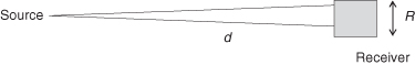
Since R > δ = αd in both x- and y-axes, signal is lost at a rate of k(1/d2).
Given the limitations, the use of laser free space (as distinct from fiber optics) for communication is probably a secondary prospect for ASOC.
8.7.2 RF
The work of the Smart Dust program seems to the most relevant and useful here [63, 181]. That program demonstrated the integration of low-power RF into an SOC chip. To summarize some of their many findings:
1. A feasibility study realized a transceiver achieving 100 Kbps over a 20-m distance with an energy budget of 25 nJ/bit. This corresponds to about 1011 bits/J/m. One joule of battery energy allows 100 Gbits to be transferred across 1 m [181].
2. Expressing data volume on a per-meter basis (as above) might imply a linear relation between signal loss and distance. This is incorrect. As with light, RF signal strength is a function of at least distance, d, squared; but it is also a function of frequency, f. At best the RF signal is proportional to k(1/fd2). In many situations the signal may be reflected and arrives at the receiver in multiple uncoordinated modes. This multipath signal represents additional signal loss. It is usually expressed as k(1/fd2)(d0/d)n, where d0 is a standard distance (usually 1 m) and typically n is 3 or 4.
3. Communications with less than 1 mW was not only feasible but likely to be commercialized. With typical duty cycle of less than 1% the average power consumption was between 1 and 10 µW.
4. There is a large data packet overhead (including start-up and synchronization, start symbol, address, packet length, encryption, and error correction). Short messages can have as little as 3% payload packet efficiency. It is better to create fewer longer messages.
5. As a result of (2) and (3), the system designer will want to minimize the number of transmissions and maximize the data packet payload.
8.7.3 Potential for Laser/RF Communications
Table 8.4 summarizes and compares the communications (data volume or total number of bits) potential per joule of energy. While laser light seems to offer more bits per joule, its limitations restrict its use.
TABLE 8.4 Comparing Communication Technologies

CHALLENGE
Adaptive and optimized communications including hyperdirectional antennae for RF and adaptive special synchronization for light and transmission.
Protocols are needed to support short broadly directional initial transmission, which enables sender and receiver to align for optimum path transmission.
8.7.4 Networked ASOC
In many situations multiple ASOCs form a network connecting an ultimate sender and receiver across several intermediate nodes. For such a system to be viable and connected, the ASOC placement must be constrained to a maximum average distance between nodes. This maximum distance depends on path loss characteristics. In RF, the Smart Dust experiment showed that this distance could vary from 1 km to 10 m as n varies from 2 to 4. It is important to remember that the message bits passed across the network comes with a (sometimes large) overhead due to synchronization. Spatial and temporal synchronization requires adaptation and signaling overhead. This can be of the order of 100 bits/message for time synchronization alone. Ideally, the system would have infrequent but long messages so as to minimize this overhead.
CHALLENGE
Communications technology that minimizes synchronization (both special and temporal) overhead.
In order to enable efficient short message communications, it is essential to reduce overhead to the order of 10s of bits rather than much more.
8.8 SENSING
8.8.1 Visual
Vision and motion sensors are usually configured as an array of photodiodes, with array sizes varying from 64 × 64 to 4000 × 4000 or more [144]. Each photodiode represents a pixel in the image (for grayscale digital images). Three or more diodes are needed for colored and multiple spectrum images. To conserve power and reduce state transitions an ASOC would probably implement the vision processor as an array with a single element per pixel.
In either image recognition or motion detection and recognition, it is necessary to find either the correspondence with a reference image or the direction in which a block in one image shifts with respect to a previous image [65]. Determining the match between two images or successive frames of the same scene requires that the image be partitioned into blocks. The blocks of one image are compared to the reference or previous image block by block in a spiral pattern. Each comparison involves computing the SAD (sum of absolute difference) index. When the image configuration with the minimum SAD index is found, the recognition or motion flow is resolved. While image recognition should be possible in milliseconds, the challenge for vision sensors is to meet the computational requirements of relatively fast-moving objects (Figure 8.7).
Figure 8.7 Visual processing.
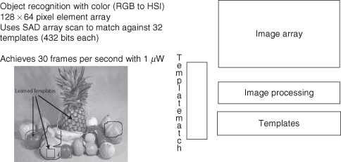
While it is clear that the image sensors can be integrated in the ASOC, optics for focusing distant object in varying amounts of light can improve performance.
8.8.2 Audio
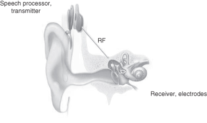
As mentioned above the piezoelectric effect applied to silicon crystal can be used to record sounds and is the basis for many simple sound detection and microphone systems. Alternatively, in specialized applications such as hearing aids, it is sometimes important to mimic the action of the ear. Various cochlear chips have been realized using a sequence of low-pass filters to emulate the operation of the cochlea. In one silicon implementation [251], 360 cells each containing dual low-pass filters are arranged as a linear array. Cochlea-type implementations are usually preferred when speech recognition is required: they form the frontend signal processing of the auditory system, separating sound waves and mapping them into the frequency domain (Figure 8.8).
Figure 8.8 Audio processing (Cochlear implant from Wikipedia).
Since audible sound frequencies are relatively low there are few real-time constraints for an ASOC.
8.9 MOTION, FLIGHT, AND THE FRUIT FLY
Of course, the ultimate ASOC can both move and fly. Given a weight of only 0.2 g motion per se is not a problem when the ASOC has associated MEMS. MEMS and nanomotors are used to anchor and move the ASOC across a surface. The energy required to move on a surface is simply the force to start (accelerate) and then to overcome friction. One joule of energy translates into 107 ergs. An erg is the energy required to move a gram for 1 cm with the force of a dyne. So slow motion (order of 1–2 cm/s) that occurs relatively infrequently (less than 1% duty cycle) should not cause significant ASOC energy dissipation.
The motion of flight is by far the most complex. Various attempts [273] have been made for small vehicle autonomous flight. Flight encapsulates many of the ASOC challenges: power, vision (avoiding obstructions), environment (wind, etc.), and communications. While the flying ASOC is a way off, such systems are feasible as any small fruit fly [209] knows!
It is interesting to note that even the ambitious ASOC described here has modest specifications when compared with biological creatures such as a fruit fly (Figure 8.9). A fruit fly has a typical length of 2.5 mm, occupies a volume of 2 mm3, and weighs less than 20 mg. Typically it has only a 1-month lifetime.
Figure 8.9 The fruit fly (from Wikipedia).
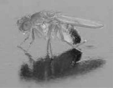
Its vision processing is quite impressive. It has 800 vision receptor units, each with eight photoreceptors for colors through the ultraviolet (using 200,000 neurons out of a total of about 1 million). It is estimated that it has 10 times better temporal vision than the human vision system. When coupled with processing for olfaction, audition, learning/memory, and communications with other nodes (flies), it represents an elegant ASOC. Its ability in flight just further impresses: its wings beat 220 times per second and can move at 10 cm/s and rotate 90 degrees in 50 ms. Its energy source is scavenged rotting fruit.
There have been recent proposals about the development of robotic flies with control systems inspired by the real ones [255]. Clearly the designer of silicon-based ASOC described here has much to learn from the fruit fly.
CHALLENGE
Sensor miniaturization and integration of transducers for measurement of temperature and strain, and movement and pressure.
At present, there is an assumption that these units will be off die and hence large. At issue is how to miniaturize and integrate these into an ASOC.
II. THE FUTURE DESIGN PROCESS: SELF-OPTIMIZATION AND SELF-VERIFICATION
8.10 MOTIVATION
The remaining sections of this chapter cover an approach that can be used to develop advanced SOC including the ASOC described earlier.
A good design is efficient and meets requirements. Optimization enhances efficiency, while verification demonstrates that requirements are met. Unfortunately, many existing designs are either inefficient, incorrect, or both.
Optimization and verification are recognized to be of major importance at all levels of abstraction in design. A recent International Technology Roadmap for Semiconductors listed “cost-driven design optimization” and “verification and testing” as two of the three overall challenges in design; the remaining challenge is “reuse.”
What would a future be like in which these three challenges are met? Let us imagine that building blocks for use in design are endowed with the capability of optimizing and verifying themselves. A new design can be completed in the following ways:
1. Characterize the desired attributes of the design that define the requirements, such as its function, accuracy, timing, power consumption, and preferred technology.
2. Develop or select an architecture that is likely to meet the requirements and explore appropriate instantiations of its building blocks.
3. Decide whether existing building blocks meet requirements; if not, either start a new search, or develop new optimizable and verifiable building blocks, or adapt requirements to what can be realized.
4. After confirming that the optimized and verified design meets the requirements, organize the optimization and verification steps to enable the design to become self-optimizing and self-verifying.
5. Generalize the design and the corresponding self-optimization and self-verification capabilities to enhance its applicability and reusability.
A key consideration is to be able to preserve self-optimization and self-verification in the design process: starting from components with such properties, the composite design is also self-optimizing and self-verifying. In the next few sections, we include more information about this approach.
8.11 OVERVIEW
Optimization can be used to transform an obvious but inefficient design into one that is efficient but no longer obvious. Verification can then show, for instance, that the optimization preserves functional behavior subject to certain preconditions. A common error in design is to apply optimizations disregarding such preconditions. Verification can also be used to check whether a design possesses desirable properties, such as safety and security, to a particular standard.
Optimization and verification, when combined with a generic design style, supports reuse in three main ways. First, an optimized generic design provides abstraction from details, enabling designers to focus on the available optimization options and their effects. Second, a generic design offers choices at multiple levels of abstraction, from algorithms and architectures to technology-specific elements. Third, a verified optimization process improves confidence in the correctness of its optimized designs. Correctness must be established before a design can be reused. In the event of errors, one can check whether the verification is incorrect or whether the design is applied in a context outside the scope of the verification.
We take a broad view of self-optimization and self-verification. One way is to think of a design—which can include both hardware and software—and its characterization about the key properties that an implementation should possess. Such properties include functional correctness, type compatibility, absence of arithmetic underflow or overflow, and so on. The characterization can include prescriptions about how the design can be optimized or verified by specific tools locally or remotely. Various mechanisms, from script-driven facilities to machine learning procedures, can be used in the self-optimization and self-verification processes, making use of context information where available. Designers can focus on optimizing and verifying particular aspects; for instance, one may wish to obtain the smallest design for computing Advanced Encryption Standard (AES) encryption on 128-bit data streams with a 512-bit key at 500 MHz.
The proposed design flow involves self-optimization and self-verification before and after deployment (Table 8.5). Before deployment, compilation produces an initial implementation and its characterization. The characterization contains information about how the design has been optimized and verified, and also about opportunities for further optimization and verification; such opportunities can then be explored after deployment at run time for a particular context to improve efficiency and confidence of correctness.
TABLE 8.5 Context for Predeployment and Postdeployment
| Predeployment | Postdeployment | |
| Focus context | Designer productivity design tool environment, often static | Design efficiency operation environment, often dynamic |
| Acquire context | From parameters affecting tool performance | From data input, for example, sensors |
| Optimize/verify | Optimize/verify initial postdeployment design | Optimize according to situation |
| Planning | Plan postdeployment optimize/verify | Plan to meet postdeployment goals |
| External control | Frequent | Infrequent |
The self-optimization of a design depends on context. Before deployment, the context is the design tool environment; the context can be acquired by identifying parameters that affect design tool performance. While automated facilities, possibly self-improving, attempt to figure out what combinations of libraries and tools would produce a design that best meets the requirements, designers can optionally control the tools to ensure such self-optimization and self-verification proceed in the right direction. In contrast, after deployment such external control is usually less frequent, for instance if the design is part of a spacecraft. To summarize, predeployment tasks are mainly strategic and try to proactively determine possible courses of action that might take place at run time; postdeployment tasks are mainly tactical and must choose between the set of possible actions to react to the changing run-time context.
Our approach has three main benefits. First, it enhances confidence in design correctness and reliability by automating the verification process. Second, it improves design efficiency by automating the optimization process and exploiting run-time adaptivity. Third, it raises productivity by enabling reuse of designs and their optimization and verification.
However, adopting systematic design reuse—especially when self-optimization and self-verification are involved—can require more initial effort than doing a one-off design. The designer needs to organize, generalize, and document the designs appropriately. Only after some time, design reuse would become worthwhile (Figure 8.10). Moreover, there can be large overheads involved in supporting optimization and verification after deployment. In the long term, however, those who invest in capabilities for design reuse and design adaptability are likely to achieve substantial improvement in design efficiency and productivity.
Figure 8.10 Design effort: The impact of reuse.

CHALLENGE
Capture composable generic descriptions of design and context, together with their optimization and verification characterization, at various levels of abstraction.
Composition is a convenient way of reuse, but it may not be straightforward, other than for those that adopt simple communication regimes such as streaming. In particular, before composing heterogeneous components, they may need to be transformed to support a common communication and synchronization infrastructure. System-level design composition is challenging, since not only the designs themselves are composed, but also their corresponding optimization and verification procedures.
8.12 PRE-DEPLOYMENT
Before deployment, a designer has the characterization of a desired design and has access to building blocks and their characterization. The task is to develop an architecture that defines how selected building blocks are instantiated and composed to produce an initial design that either meets the requirements, or can be further optimized to do so, after deployment at run time. Postdeployment optimization and verification have to be planned carefully to avoid becoming an unaffordable overhead.
We assume that, at compile time before deployment,
1. the available computing resources are adequate to support the design and the tools, but
2. there is a limit on how much optimization and verification can take place since, for instance, some data values useful for optimization are only known at run time, and it is impractical to compute all possibilities for such values.
As a simple example, given that one of the two operands of an n-bit adder is a constant whose value is only known after deployment at run time, we wish to optimize the adder by constant propagation. It is, however, impractical to precompute the configuration of all 2n possibilities, unless n is a small number. Fortunately, if we target a bit-slice architecture, then it may suffice to precompute only two configurations for each of the n bits so that, at run time when the value is known, the appropriate configuration can be placed at the right location at the right time [216].
Designers may have to prioritize or to change their requirements until a feasible implementation is found. For instance, one may want the most power-efficient design that meets a particular timing constraint or the smallest design that satisfies a given numerical accuracy. Other factors, such as safety or security issues, may also need to be taken into account.
Given that predeployment optimization is to produce an optimized design that would, where appropriate, be further optimized after deployment, the following are some examples of optimizations that can take place before deployment:
1. Choose a circuit technology in which the design would be implemented. The two common technologies are application-specific integrated circuit (ASIC) and field-programmable gate array (FPGA); the choice of technology depends on volume and flexibility (Figure 8.11). For instance, cell-based ASIC tends to be cheaper at large volume since they have large nonrecurring engineering cost, while FPGA is the other way around with structured ASIC somewhere in between. While ASIC technology can be used to implement adaptive instruction processors with, for instance, custom instruction extensions [29] or a reconfigurable cache [76], all the options for reconfiguration have to be known before fabrication. Adaptive instruction processors can also be implemented in FPGA technology [77, 269], which allows them much more flexibility at the expense of speed and area overheads in supporting reconfigurability.
2. Choose the granularity and synchronization regime for the configurable units. Current commercial FPGAs are mainly fine-grained devices with one or more global clocks, but other architectures are emerging: there are coarse-grained devices containing an array of multi-bit ALUs (arithmetic logic units) executing in parallel [25, 80], as well as architectures based on self-synchronizing technology to enhance scalability [52]. Generally, fine-grained devices have a better chance to be tailored to match closely with what is required. For instance, if a 9-bit ALU is needed, nine bit-level cells in an FPGA would be configured to form that 9-bit ALU. For a coarse-grained device containing cells with 8-bit ALUs, two such cells would be needed. However, fine-grained devices tend to have a large overhead in speed, area, power consumption, and so on, since there are more resources that can be configured. Coarse-grained devices, in contrast, have lower overheads at the expense of flexibility.
3. For instruction processors with support for custom instructions [29, 77], choose the granularity of custom instructions to achieve the right balance between speed and area. Coarse-grained custom instructions are usually faster but require more area than fine-grained ones. For instance, if the same result can be achieved using: (a) one coarse-grained custom instruction, or (b) 50 fine-grained custom instructions, then (a) is likely to be more efficient since there are fewer instruction fetch/decode, and there are more opportunities to customize the instruction to do exactly what is needed. However, since the more coarse-grained an instruction, the more specific it can become, there would be fewer ways for reusing a coarse-grained custom instruction than a fine-grained one.
4. Choose the amount of parallelism and hardware/software partitioning to match performance or size constraints by determining, for instance, the number of processing elements, the level of pipelining, or the extent of task sharing for each processing element. Various factors, such as the speed and size of control logic and on-chip memory, and interfaces to other elements such as memory or sensors, would also need to be taken into account. As an example, Figure 8.12 shows how speedup varies with the number of processors targeting an FPGA for a multiprocessor architecture specialized for accelerating inductive logic programming applications [89]. Since the amount of FPGA on-chip memory is fixed, increasing the number of processors reduces the amount of cache memory for each processor; hence, the linear speedup until there are 16 processors. After this optimal point, adding more processors reduces the speedup since the cache for each processor becomes too small.
5. Choose data representations and the corresponding operations. Trade-offs in adopting different kinds of arithmetic representations are well known: for instance, redundant arithmetic tends to produce faster designs, since no carry chain is required at the expense of size. Since fine-grained FPGAs support designs with any word length, various static and dynamic word-length optimization algorithms can be used for providing designs with the best trade-off between performance, size, power consumption, and accuracy in terms of, for instance, signal-to-noise ratio [62]. Models and facilities to support exceptions, such as arithmetic overflow and underflow, should also be considered [153].
6. Choose placement strategies for processing and memory elements on the physical device, such as those interacting frequently are placed close to one another to improve performance, area, and power consumption. It may be possible to automate the optimization of placement by a combination of heuristics and search-based autotuners [27] that generate and evaluate various implementation options; such methods would need to take into account various architectural constraints, such as the presence of embedded computational or memory elements [36].
Figure 8.11 Comparing cost and volume for FPGA and ASIC technologies.
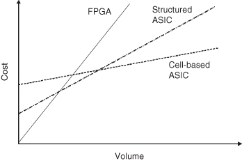
Figure 8.12 Variation of speedup and aggregate miss rate against the number of processors for the Arvand multiprocessor system targeting the XC2V6000 FPGA.

Each example above has aspects that would benefit from verification, from high-level compilation [43] to flattening procedures [168] and placement strategies [196]. There are verification platforms [236] enabling consistent application of verification facilities such as symbolic simulators, model checkers, and theorem provers. Such platforms show promise in supporting self-verification for complex designs, but much remains to be done to verify designs involving various technologies and across multiple levels of abstraction. Also, many of these platforms and facilities may be able to benefit from automatic tuning [121].
One important predeployment task is to plan self-optimization and self-verification after deployment. This plan would depend on how much run-time information after deployment is available. For instance, if some inputs to a design are constant, then such constants can be propagated through the design by boolean optimization and retiming. Such techniques can be extended to cover placement strategies for producing parametric descriptions of compact layout [168]. Another possibility is to select appropriate architectural templates to facilitate run-time resource integration [211].
Before deployment, if verification already covers optimizations and all other postdeployment operations, then there is no need for further verification. However, if certain optimizations and verifications are found useful but cannot be supported by the particular design, it may be possible for such optimizations and verifications to take place remotely, so that the optimized and verified design would be downloaded securely into the running system at an appropriate time, minimizing interruption of service.
CHALLENGE
Develop techniques and tools for specifying and analyzing requirements of self-optimizing and self-verifying systems, and methods for automating optimization and verification of operations and data representations.
Relevant optimization techniques include scheduling, retiming, and word-length optimization, while relevant verification techniques include program analysis, model checking, and theorem proving. Their effective tuning and combination, together with new methods that explore, for instance, appropriate arithmetic schemes and their impact, would enable efficient designs to be produced with reduced effort.
8.13 POST-DEPLOYMENT
The purpose of optimization is to tailor a design to best meet its requirements. Increasingly, however, such requirements no longer stay the same after the design is commissioned; for instance, new standards may need to be met, or errors may need to be fixed. Hence there is a growing need for upgradable designs that support postdeployment optimization. Besides upgradability, postdeployment optimization also enables resource sharing, error removal, and adaptation to run-time conditions—for instance, selecting appropriate error-correcting codes depending on the noise variation.
Clearly any programmable device would be capable of postdeployment optimization. As we described earlier, fine-grained devices have greater opportunities of adapting themselves than coarse-grained devices, at the expense of larger overheads.
In the following we focus on two themes in postdeployment optimization: situation-specific optimization and autonomous optimization control. In both cases, any untrusted postdeployment optimizations should be verified by lightweight verifiers; possible techniques include proof-carrying code checkers [252]. Such checkers support parameters that capture the safety conditions for particular operations. A set of proof rules are used to establish acceptable ways of constructing the proofs for the safety conditions.
As mentioned in the preceding section, should heavy-duty optimizations and verifications become desirable, it may be possible for such tasks to be carried out by separate trusted agents remotely and downloaded into the operational device in a secure way, possibly based on digital signatures that can verify senders’ identity. Otherwise it would be prudent to include a time-out facility to prevent nontermination of self-optimization and self-verification routines that do not produce results before completion.
Besides having a time-out facility, postdeployment verification should be capable of dealing with other forms of exceptions, such as verification failure or occurrence of arithmetic errors. There should be error recovery procedures, together with techniques that decide whether to avoid or to correct similar errors in the future. For some applications, on-chip debug facilities [120] would be useful; such facilities can themselves be adapted to match the operational and buffering requirements of different applications.
8.13.1 Situation-Specific Optimization
One way to take advantage of postdeployment optimization in a changing operational environment is to continuously adapt to the changing situation, such as temperature, noise, process variation, and so on. For instance, it has been shown [241] that dynamic reconfiguration of a Viterbi decoder to adapt the error-correcting convolutional codes to the variation of communication channel noise conditions can result in almost 70% reduction in decoder power consumption, with no loss of decode accuracy.
Figure 8.13 shows a reconfiguration schedule that optimally adapts to the program phase behavior of the SPECviewperf benchmark 9 [232]. A program phase is an interval over which the working set of the program remains largely constant; our purpose is to support a dynamic optimization regime that makes use of program phase information to optimize designs at run time. The regime consists of a hardware compilation scheme for generating configurations that exploit program branch probability [231] and other opportunities to optimize for different phases of execution, and a run-time system that manages interchange of configurations to maintain optimization between phase transitions. The idea is to accelerate the hardware for branches that occur frequently in a particular program phase; when the beginning of the next program phase is detected, the hardware would be reconfigured to optimize the new program phase.
Figure 8.13 Optimal reconfiguration schedule for upper bound performance measure, SPECviewperf benchmark 9. The dotted and solid lines show, respectively, the branch probabilities of the inner and outer loop over time.

In addition to improving performance by exploiting, for instance, program phase behavior, postdeployment optimization also has the potential to improve power consumption. Figure 8.14 shows a possible variation of power consumption over time. Comparing to a static design, a postdeployment optimizable design can be configured to a situation-specific design with the lowest possible power consumption for that situation, although there could be power surges when the device is being reconfigured. Techniques have been proposed for FPGAs that would automatically adjust their run-time clock speed [49] or exploit dynamic voltage scaling [57]; related methods have been reported for microprocessors [73]. Such techniques would be able to take advantage of run-time conditions after deployment, as well as adapting to effects of process variation in deep submicron technology.
Figure 8.14 Possible variation of instantaneous power consumption over time. The two narrow spikes indicate power consumption during two reconfigurations for run-time optimization.

A useful method for supporting situation-specific optimization is to integrate domain-specific customizations into a high-performance virtual machine, to which both static and dynamic information from postdeployment instrumentation is made available. Such information can be used in various situations for self-optimization and self-verification, such as optimizing the way hardware or software libraries are used based on special properties of the library code and context from postdeployment operation.
8.13.2 Autonomous Optimization Control
“Autonomic computing” [139] has been proposed for systems that support self-management, self-optimization, and even self-healing and self-protection. It is motivated by the increasing complexity of computer systems that require significant efforts to install, configure, tune, and maintain. In contrast, we focus on the design process that can support and benefit from self-optimizing and self-verifying components.
An evolving control strategy for self-optimization can be based on event-driven, just-in-time reconfiguration methods for producing software code and hardware configuration information according to run-time conditions, while hiding configuration latency. One direction is to develop the theory and practice for adaptive components involving both hardware and software elements, based on component metadata description [138]. Such descriptions characterize available optimizations and provide a model of performance together with a composition metaprogram that uses component metadata to find and configure the optimum implementation for a given context. This work can be combined with current customizable hardware compilation techniques [245], which make use of metadata descriptions in a contract-based approach, as well as research on adaptive software component technology.
Another direction is to investigate high-level descriptions of desirable autonomous behavior and how such descriptions can be used to produce a reactive plan. A reactive plan adapts to a changing environment by assigning an action toward a goal for every state from which the goal can be reached [238]. Dynamic reconfiguration can be driven by a plan specifying the properties a configuration should support.
Other promising directions for autonomous optimization control include those based on machine learning [6], inductive logic programming [89], and self-organizing feature maps [200]. Examples of practical self-adaptive systems, such as those targeting space missions [140], should also be studied to explore their potential for widening applicability and for inspiring theoretical development. It would be interesting to find an appropriate notion of verifiability for these optimization methods.
CHALLENGE
Find strategies that provide the best partitioning between co-optimization and coverification before and after deployment.
The more work is done before deployment, the more efficient the postdeployment design for a given application tends to become, but at the expense of flexibility. Strategies for getting the right balance between predeployment and postdeployment optimization and verification will be useful.
8.14 ROADMAP AND CHALLENGES
In the short term, we need to understand how to compose self-optimizing and self-verifying components, such that the resulting composite design is still self-optimizing and self-verifying. A key step is to provide both theoretical and practical connections between relevant design models and representations, as well as their corresponding optimization and verification procedures, to ensure consistency between semantic models and compatibility between interfaces of different tools.
It seems a good idea to begin by studying self-optimizing and self-verifying design in specific application domains. Experience gained from such studies would enable the discovery of fundamental principles and theories concerning the scope and capability of self-optimizing and self-verifying design that transcend the particularities of individual applications.
Another direction is to explore a platform-based approach for developing self-optimizing and self-verifying systems. Promising work [236] has been reported in combining various tools for verifying complex designs; such work provides a basis on which further research on self-optimization and self-verification can be built. Open-access repositories that enable shared designs and tools would be useful; in particular, the proposed approach would benefit from, and also contribute to, the verified software repository [43], currently being developed as part of the UK Grand Challenge project in dependable systems evolution.
Clearly, much research remains to be done to explore the potential for self-optimizing and self-verifying design. Progress in various areas is required to enhance self-optimization and self-verification for future development.
Challenge. So far, we focus on designing a single element that may operate autonomously. The criteria for optimality and correctness become more complex for a network of autonomous elements, especially if the control is also distributed. We need to develop theoretical and practical connections between the optimality and correctness of the individual elements, and the optimality and correctness of the network as a whole.
Challenge. Design reuse would only become widespread if there are open standards about the quality of the re-usable components as well as the associated optimization and verification processes. Such standards cover a collection of methods for verifying functional and performance requirements, including simulation, hardware emulation, and formal verification, at different levels of abstraction.
Challenge. There is a clear need for a sound foundation to serve as the basis for engineering effective self-optimization and self-verification methodologies that closely integrate with design exploration, prototyping, and testing. The challenge is that adaptability, while improving flexibility, tends to complicate optimization and verification.
8.15 SUMMARY
There is a whole new field to be explored based on the next generation of SOC and ASOC. As we have seen, transistor density improvements will enable a billion transistors per square centimeter. This enormous computational potential has a major limitation: limited electrical energy. There is a new direction opening in computer architecture, nanocomputing, to contrast with historical efforts in supercomputing. The target of this field is to produce the algorithms and architectural approaches for high performance at less than 1 millionth of the current levels of power dissipation, freeing the chip from external power coupling.
For untethered operation, a form of wireless communication is required. This is another significant challenge, especially with a power budget also in the order of microwatts. While RF is the conventional approach, some form of light or infrared may offer an alternative.
In addition, digitizing the sensors and even the transducers offers a final challenge where multiple sensors are integrated into a seamless SOC.
The chapter also projects a vision of design with self-optimizing and self-verifying components, to address the design challenges identified by the International Technology Roadmap for Semiconductors. Tasks for self-optimization and self-verification before and after deployment are described, together with a discussion of possible benefits and challenges. Making progress in theory and practice for self-optimization and self-verification would contribute to our goal: enabling designers to produce better designs more rapidly.
The best designs anticipate system complexity and deal effectively with the unanticipated. System complexity includes many issues overlooked in this chapter: component design and suppliers, design tools, validation and testing, security, and so on. Successful trade-offs across a myriad of issues define effective design.
While there is little expectation that all of the ASOC components discussed here will actually be integrated into a single die, there are many different possible combinations. Each combination with its own system requirements must be optimized across all of the constituent components. Designers, with the help of a self-optimizing and self-verifying development approach, are now no longer concerned about a component but only about the final system; they become the ultimate systems engineers.