7
Application Studies
7.1 INTRODUCTION
This chapter describes various applications to illustrate the opportunities and trade-offs in SOC design. It also shows how some of the techniques described in earlier chapters can be applied.
We first present an approach for developing SOC designs. Then we illustrate the proposed techniques in analyzing simple designs for the Advanced Encryption Standard (AES). Next, we have a look at 3-D computer graphics, showing the use of analysis and prototyping techniques and their application to a simplified PS2 system. After that we describe compression methods for still image and real-time video, as well as a few other applications to illustrate the variety of requirements and architectures of SOCs.
Our discussion separates requirements from designs that can be shown to meet the requirements. Requirements cover what are needed, while a design includes sufficient implementation detail for it to be evaluated against the requirements.
7.2 SOC DESIGN APPROACH
Figure 7.1 shows a simplified SOC design approach based on the material from the preceding chapters. Chapter 2 introduces five big issues in SOC design: performance, die area, power consumption, reliability, and configurability. These issues provide the basis on which design specification and run-time requirements for SOC designs can be captured. An initial design can then be developed, which would show promise in meeting the key requirements. This initial design can then be systematically optimized by addressing issues related to memory (Chapter 4), interconnect (Chapter 5), processor (Chapter 3) and cache (Chapter 4), and customization and configurability (Chapter 6). This process is repeated until reaching a design that meets the specification and run-time requirements. More details will be given later in this section.
Figure 7.1 An approach for designing SOC devices.

Following this approach, however, can appear to be a formidable task. System design is often more challenging than component or processor design, and it often takes many iterations through the design to ensure that (1) the design requirements are satisfied and (2) the design is close to optimal, where optimality includes considerations for overall cost (including design, manufacturing, and other costs) and performance (including market size and competition).
The usual starting point for a design is an initial project plan. As discussed in Chapter 1, this includes a budget allocation for product development, a schedule, a market estimate (and a corresponding competitive product analysis), and some measure of targeted product performance and cost. As shown in Figure 7.2, the next step is to create an initial product design. This design is merely a placeholder (or “straw man”) that has a good chance of meeting requirements in target product performance and cost. Further analysis may prove that it may or may not satisfy the requirements. An important part of this initial analysis is to develop a complete understanding of the performance and functional requirements and their inter-relationship. The various pieces of the application are specified and formally defined, and appropriate analytic and simulation models are developed. These models should provide an idea of the performance–functionality trade-off for the application and the implementation technology, which would be important in meeting run-time requirements such as those shown in Table 7.1.
TABLE 7.1 Run-Time Requirements Showing Various Constraints to Be Met for Some Video and Graphics Applications
| Application | Real-Time Constraint (fps) | Other Constraints |
| Video conference | 16 | Frame size, error rate, missed frames |
| 3-D graphics | 30 | Image size, shading, texture, color |
Figure 7.2 The system design process.

REQUIREMENTS AND DESIGN
The input to the requirement understanding task is usually a requirement specification from customers or from a marketing study. The output is often a functional requirement specification for the design. The specification may be detailed and carefully written for review; this is the case in large companies. However, the specification may also be brief, captured, for example, in a spreadsheet; this is often the case in small companies and startups. The specification, whether detailed or brief, is essential for design review, documentation, and verification, and must be clear and consistent. Moreover, mathematical, executable, or diagrammatic descriptions can be used to capture data flow and control flow for the main operations or selected functions of the SOC, during various system design stages. Such descriptions can help designers to understand the functional requirements. Once the functional requirements are understood, these descriptions can be mapped to possible implementations of the main components and their interactions in the SOC.
With the design specification ready, we propose an initial system design (Figure 7.3). Design specifications usually anticipate the general product layout, addressing issues such as having all on one die or system on a board, operating system selection, total size of memory, and backing store. The development of the initial design then proceeds as follows, to ensure that the critical requirements are met:
1. Selection and allocation of memory and backing store. This generally follows the discussions in Chapter 4.
2. Once the memory has been allocated, the processor(s) are selected. Usually a simple base processor is selected to run the operating system and manage the application control functions. Time critical processes can be assigned to special processors (such as VLIW and SIMD processors discussed in Chapter 1 and Chapter 3) depending on the nature of the critical computation.
3. The layout of the memory and the processors generally defines the interconnect architecture covered in Chapter 5. Now the bandwidth requirements must be determined. Again the design specifications and processor target performance largely determine the overall requirement but cache memory can act as an important buffer element in meeting specifications. Usually the initial design assumes that the interconnect bandwidth is sufficient to match the bandwidth of memory.
4. The memory elements are analyzed to assess their effects on latency and bandwidth. The caches or data buffers are sized to meet the memory and interconnect bandwidth requirements. Some details can be covered later, so for instance bus latency is usually determined without considering the effects of bus contention. Processor performance models are developed.
5. Some applications require peripheral selection and design, which must also meet bandwidth requirements. Example peripherals are shown in Section 7.5.1, which covers the JPEG system for a digital still camera, and also in Section 8.7, which covers radio frequency and optical communications for future autonomous SOCs.
6. Rough estimates of overall cost and performance are determined.
Figure 7.3 An example of an initial design, with three processors P1, P2, and P3.

Following initial design, the design optimization and verification phase begins. This phase is supported by various tools, including profiling facilities and optimizing compilers. All components and allocations are reassessed with the view toward lowering cost (area) and improving both performance and functionality. For instance, customization and configurability techniques, such as the use of custom instructions or the adoption of run-time reconfiguration as discussed in Chapter 6, can be applied to enhance flexibility or performance. As another example, software optimizations, such as those that improve locality of reference, can often provide large performance improvement for little hardware cost. The optimization would, where applicable, involve repartitioning between hardware and software, which could affect the complexity of embedded software programs [151] and the choice of real-time operating systems [34].
After each optimization, its impact on accuracy, performance, resource usage, power and energy consumption, and so on needs to be analyzed. Also the design needs to be verified to make sure that its correctness would not be affected by the optimizations [53]. Such analysis and verification can often be supported by electronic system-level design tools (see box), as well as by prototyping.
ESL: ELECTRONIC SYSTEM LEVEL DESIGN AND VERIFICATION
There does not seem to be a standard description of what ESL covers. Wikipedia describes ESL design and verification to be “an emerging electronic design methodology that focuses on the higher abstraction level concerns first and foremost.” Another definition of ESL is the utilization of appropriate abstractions in order to increase comprehension about a system, and to enhance the probability of a successful implementation of functionality in a cost-effective manner [32]. Various ESL tools have been developed, which are capable of supporting a design flow that can generate systems across hardware and software boundaries from an algorithmic description [108].
When the design appears optimal after several iterations, another complete program plan is developed to understand any changes made to schedule fixed costs and to address issues involved in system integration and testing. Finally, the product market is assessed based on the final design and the overall program profitability can be assessed.
7.3 APPLICATION STUDY: AES
We adopt the AES as a case study to illustrate how techniques discussed in the preceding chapters can be used for exploring designs that meet specified requirements.
7.3.1 AES: Algorithm and Requirements
The AES cipher standard [69] has three block sizes: 128 (AES-128), 192 (AES-192), and 256 (AES-256) bits. The whole process from original data to encrypted data involves one initial round, r − 1 standard rounds, and one final round. The major transformations involve the following steps (Figure 7.4):
- SubBytes. An input block is transformed byte by byte by using a special design substitution box (S-Box).
- ShiftRows. The bytes of the input are arranged into four rows. Each row is then rotated with a predefined step according to its row value.
- MixColumns. The arranged four-row structure is then transformed by using polynomial multiplication over GF (28) per column basis.
- AddRoundKey. The input block is XOR-ed with the key in that round.
Figure 7.4 Fully pipelined AES architecture [107].

There is one round AddRoundKey operation in the initial round; the standard round consists of all four operations above; and the MixColumns operation is removed in the final round operation, while the other three operations remain. On the other hand, the inverse transformations are applied for decryption. The round transformation can be parallelized for fast implementation.
Besides the above four main steps, the AES standard includes three block sizes: 128 (AES-128), 192 (AES-192), and 256 (AES-256) bits. The whole block encryption is divided into different rounds. The design supporting AES-128 standard consists of 10 rounds.
Run-time requirements are shown in Table 7.2 for various applications, such as Wi-Fi and VoIP (Voice over Internet Protocol); our task is to find designs that meet one or more of these throughput requirements.
TABLE 7.2 Different Application Throughput Requirements, PAN: Personal Area Network
| Application | Throughput requirement |
| Wi-Fi 802.11b | 11 Mbps |
| Wi-Fi 802.11g | 54 Mbps |
| Wi-Fi 802.11i/802.11n | 500 Mbps |
| Metropolitan area network (MAN) 802.16a | 75 Mbps |
| PAN 802.15 TG4 (low rate) | 250 Kbps |
| PAN 802.15 TG3 (high rate) | 55 Mbps |
| VoIP | 64 Kbps |
| Cisco PIX firewall router | 370 Mbps |
7.3.2 AES: Design and Evaluation
Our initial design starts with a die size, design specification, and run-time requirement (Figure 7.1). We assume that the requirements specify the use of a PLCC68 (Plastic Leaded Chip carrier) package, with a die size of 24.2 × 24.2 mm2.
Our task is to select a processor that meets the area constraint while capable of performing a required function. Let us consider ARM7TDMI, a 32-bit RISC processor. Its die size is 0.59 mm2 for a 180 nm process, and 0.18 mm2 for a 90 nm process. Clearly, both processors can fit into the initial area requirement for the PLCC68 package. The cycle count for executing AES from the SimpleScalar tool set is 16,511, so the throughput, given an 115-MHz clock (as advertised by the vendor) with the 180-nm device, is (115 × 32)/16,511 = 222.9 Kbps; for a 236-MHz clock with the 90-nm device, the throughput is 457.4 Kbps. Hence the 180-nm ARM7 device is likely to be capable of performing only VoIP in Table 7.2, while the 90 nm ARM7 device should be able to support PAN 802.15 TG4 as well.
Let us explore optimization of this SOC chip such that we can improve the total system throughput without violating the initial area constraint. We would apply the technique used in Chapter 4 for modifying the cache size and evaluate its effect, using facilities such as the SimpleScalar tool set [30] if a software model for the application is available.
Using SimpleScalar with an AES software model, we explore the effects of doubling the block size of a 512-set L1 direct mapped instruction cache from 32 bytes to 64 bytes; the AES cycle count reduces from 16,511 to 16,094, or 2.6%. Assume that the initial area of the processor with the basic configuration without cache is 60K rbe, and the L1 instruction cache has 8K rbe. If we double the size of the cache, we get a total of 76K rbe instead of 68K. The total area increase is over 11%, which does not seem worthwhile for a 2.6% speed improvement.
The ARM7 is already a pipelined instruction processor. Other architectural styles, such as parallel pipelined datapaths, have much potential as shown in Table 7.3; these FPGA designs meet the throughput requirements for all the applications in Table 7.2, at the expense of larger area and power consumption than ASICs [146]. Another alternative, mentioned in Chapter 6, is to extend the instruction set of a processor by custom instructions [28]; in this case they would be specific to AES.
TABLE 7.3 Performance and Area Trade-off on a Xilinx Virtex XCV-1000 FPGA [107]

BRAM: block RAM. Note that a fully pipelined design requires more resources than the XCV-1000 device can support.
A note of caution: the above discussion is intended to illustrate what conclusions can be drawn given a set of conditions. In practice, various other factors should be taken into account, such as how representative are the numbers derived from, for instance, benchmark results or application scenarios based on the SimpleScalar tool set. In any case, such analysis should only be used for producing evaluations similar to those from back-of-envelope estimates—useful in providing a feel for promising solutions, which should then be confirmed by detailed design using appropriate design tools.
Two further considerations. First, as shown in Figure 7.4, an AES design can be fully pipelined and fitted into an FPGA device. To achieve over 21 Gbit/s throughput, the implementation exploits technology-specific architectures in FPGAs, such as block memories and block multipliers [107].
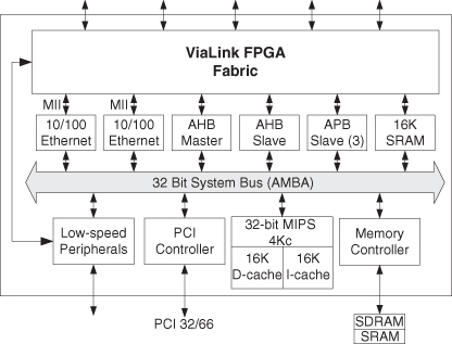
Second, AES cores are often used as part of a larger system. Figure 7.5 shows one such possibility for implementing the AES core, in the ViaLink FPGA fabric on a QuickMIPS device [116]. This device has a separate 32-bit MIPS 4Kc processor core and various memory and interface elements. Another possibility is to use AES in the implementation of designs involving secure hash methods [88].
Figure 7.5 QuickMIPS block diagram for the AES SOC system [116].
7.4 APPLICATION STUDY: 3-D GRAPHICS PROCESSORS
This section considers 3-D graphics accelerators, similar to the Sony PS2 architecture [237]. Our study illustrates two useful techniques in deriving an initial design:
- Analysis. The application is viewed as a high-level algorithm for back-of-envelope-type estimates about, for instance, the amount of computation and communication so that a preliminary choice of design styles and components can be made.
- Prototyping. A simplified version of the application is developed using common software tools and off-the-shelf hardware platforms, for example using a standard PC or a general-purpose FPGA platform. The experience gained will suggest areas that are likely to require attention, such as performance bottlenecks. It may also help identify noncritical components that do not need to be optimized, saving development time.
The analysis and prototyping activities can often be assisted by ESL techniques and tools [32, 108].
7.4.1 Analysis: Processing
In 3-D graphics, objects are represented by a collection of triangles in 3-D space, and there are lighting and texture effects on each picture element—or pixel—to make objects look realistic. Such 3-D representations are transformed into a 2-D space for viewing. Animation consists of providing successive frames of pixels over time.
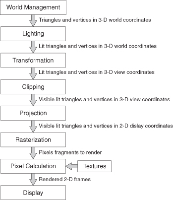
There are two main stages in the graphics pipeline (Figure 7.6): transformation and lighting, and rasterization. We cover them in turn.
Figure 7.6 3-D graphics pipeline.
Requirements
For transformation and lighting, consider v visible triangles per frame, and l light sources; the realism and complexity of the objects improve with larger v and l. To facilitate perspective projection, a system of four coordinates is used: three space dimensions and one homogeneous component capturing the location of the plane to which the 3-D image is projected.
During transformation and lighting, each triangle vertex is transformed from world space to view space, requiring a 4 × 4 matrix multiplication; then projected into 2-D, requiring a division and a further four multiplies for perspective correction. This can be approximated as about 24 FMACs (floating-point multiply and accumulate) per vertex, where a floating-point division (FDIV) is assumed to take the equivalent of four FMACs. The lighting process requires another 4 × 4 multiplication to rotate the vertex normal, followed by a dot product and some further calculations. This is approximated as 20 FMACs per light source. This results in 24 + 20l FMACs per vertex. In the worst case of three distinct vertices per triangle, v(72 + 60l) FMACs are needed per frame; if vertices between adjacent triangles can be shared, we would only need v(24 + 20l) in the best case.
Let n be the number of triangles processed per second and m be the number of FMAC per second. Given there are f frames per second (fps), n = fv and:
(7.1)
![]()
If n = 50M (M = 106) triangles per second and no lights (l = 0), then 1200M ≤ m ≤ 3600M; if n = 30 × 106 triangles per second and with one light (l = 1), then 1320 M ≤ m ≤ 3960M.
Design
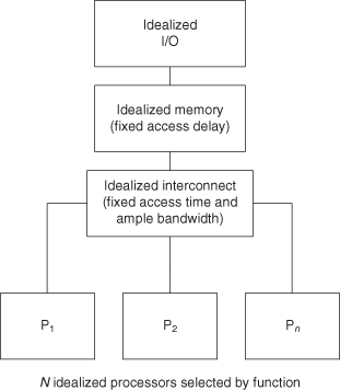
Let us describe how we come up with a design that meets the requirements. Our initial design is based on the simple structure in Figure 7.7, introduced in Chapter 1.
Figure 7.7 Idealized SOC architecture.
The proposed design is inspired by the Emotion Engine, which contains two groups of processors as shown in Figure 7.8. The first group of processors includes:
- CPU, a MIPS-III processor with 32 registers, 128 bits, dual issue;
- Floating-point unit (FPU), supporting basic FMAC and floating-point division;
- VPU0, a vector processing unit that can operate as a slave to the MIPS or as an independent SIMD/VLIW processor.
- IPU, an image processing unit for decoding compressed video streams.
Figure 7.8 Initial design for 3-D graphics engine.
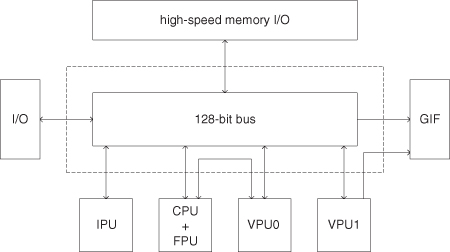
These components are connected by a 128-bit bus at 150 MHz.
The second group of processors includes:
- VPU1, the same as VPU0, but only operates as a SIMD/VLIW processor.
- GIF, a graphics interface that mainly shunts data onto the graphics synthesizer using a dedicated 128-bit bus.
Since VPU0 and VPU1 each contains four floating-point multipliers at 300 MHz, their performance is given by 300 MHz × 8 = 2400M FMAC/s; this value is within the range of 1200M ≤ m ≤ 3960M derived earlier.
There are other components that we do not cover in detail. An example is IPU, an image processing unit for decoding compressed video streams.
Requirements
The rasterization process needs to scan convert each 2-D triangle, calculating the set of output pixels corresponding to each triangle. This is usually performed by stepping vertically along the edges of the triangles using DDA (digital differential analyzer) or another line-drawing method, allowing each horizontal span to be handled at once. Within each span, it is necessary to use more DDAs to interpolate the values of Z (for occlusion testing), color, and texture coordinates where appropriate. We ignore the vertical DDAs and approximate this as requiring 2 + 2t DDA steps per pixel.
Design
If each DDA step requires four integer instructions, and the operation at each pixel (such as comparing updating frame and z-buffer) also requires four integer instructions, then the number of instructions for each rendered pixel is:
These steps must be performed each time a pixel is rendered, even if the pixel has already been rendered. Given there are o output pixels in each frame and each output pixel needs to be recalculated p times due to overlapping shapes, the total number of instructions required per frame is
We would use this result in the prototyping process below. Note that we have ignored the time taken to perform the vertical DDAs, so we would expect there to be some additional computation time that varies with v, but overall computation time is dominated by the per-pixel operation time.
7.4.2 Analysis: Interconnection
In our model of the 3-D graphics pipelines, there are two main intertask logical communications channels: lists of 3-D triangles passed from the creation/management task to the transformation task, and lists of 2-D triangles passed from the transformation task to the rendering task. Both these channels are essentially unidirectional: once a task has passed a set of triangles (2-D or 3-D) onto the next stage, there is no substantial flow of data needed in the other direction apart from obvious data flow signals such as status indicators.
Requirements
In the first channel, between world management and transformation, all the 3-D coordinates consist of three single-precision floating point components, requiring 4 × 3 = 12 bytes. The minimal triangle size, where each triangle consists only of three coordinates, requires 3 × 12 = 36 bytes. However, in most cases there will need to be additional information, such as texture information and lighting information. In order to support lighting, it is sufficient to store the surface normal at each vertex. This applies no matter how many lights are applied, so the size of each vertex then becomes 3 × (12 + 12 × min(l,1)). Texture information additionally requires the storage of a 2-D texture coordinate for each vertex; assuming floating-point texture coordinates, this adds 8 bytes to each vertex per applied texture. With n visible triangles, the total bandwidth on the channel is:
(7.4)
![]()
As an example, given n = 50 × 106, l = 0, t = 1, the bandwidth required is 3 GB/s; for n = 30 × 106, l = 1, t = 1, the bandwidth required is 2.88 GB/s.
In the second channel, each point is now in screen coordinates, so each point can be represented as two 16-bit integers. In addition the depth of each pixel is needed, but this is stored in greater precision, so the total size is 4 bytes per vertex. Assuming that lights have been applied, the vertices also require a color intensity, requiring 1 byte per channel, or approximately 4 bytes per vertex: 4 + 4 min(l,1). Each texture coordinate must still be applied individually at rasterization, so a 4-byte (2 × 16 bit integers) coordinate must be retained. This results in a total required bandwidth for the second channel as:
(7.5)
![]()
This time, given n = 50 × 106, l = 0, t = 1, the bandwidth required is 1.2 GB/s; for n = 30 × 106, l = 1, t = 1, the bandwidth required is 1.08 GB/s.
Design
As shown in Figure 7.8, the interconnect consists of a 128-bit bus. Since the peak transfer rate of a 128-bit bus at 150 MHz is 2.4 GB/s, which meets the bandwidth required for the second channel but not the first, an additional 64-bit dedicated interface to the rendering engine is included.
7.4.3 Prototyping
A prototype 3-D renderer is written in the C language. This prototype incorporates a world management stage that creates a random pattern of triangles, a transformation stage that projects triangles into 2-D using a single-precision floating point, and a z-buffer-based renderer using integer DDAs. Among the parameters of the renderer that can be varied are:
- number of triangles;
- size of triangles;
- width and height of output.
By adjusting these parameters, it is possible to selectively adjust parameters such as o, v, and p. For example, p can be varied by increasing the size of triangles, as this increases the chance that each triangle is covered by another.
Figure 7.9 shows the changes in execution time on an Athlon 1200 when the number of output pixels are increased. As expected, both the creation and transformation stages show no significant variation as the number of output pixels is increased. In contrast, the rendering stage’s execution time is clearly increasing linearly with output pixel count. The fitted line has a correlation coefficient of 0.9895, showing a good linear fit. The fitted linear relationship between rasterization time and pixel count is given by Equation 7.3: t = o × 5 × 10⁻⁸ + 0.0372. The large offset of 0.0372 is caused by the per-triangle setup time mentioned (and ignored) in the analysis section. Based on this prototype we might now feel it appropriate to include the effects, as they are clearly more significant than expected.
Figure 7.9 Increase in execution times of stages as pixel count increases.

According to Equation 7.2, the instructions per output pixel is p × 12 in the case that no textures are applied (t = 0). In this experiment P = 1.3, so the instructions per frame should be 15.6. The reported performance in million instructions per second (MIPS) of the Athlon 1200 is 1400, so according to the model each extra pixel should require 15.6/1.4 × 10−9 = 1.1 × 10⁻⁸. Comparing the predicted growth of 1.1 × 10⁻⁸ with the observed growth of 5 × 10⁻⁸, we see that they differ by a factor of 5. The majority of this error can probably be attributed to the unoptimized nature of the prototype and to the approximations in our models.
In Figure 7.10 and Figure 7.11 the performance of the transformation stage for different numbers of FPUs is tested using the PISA simulator [30]. When four multipliers are used the performance increases significantly, although there is little benefit when more than four are used. This suggests that a VLIW or SIMD processor that can perform four floating-point operations at once would be efficient. Also shown in the graph is the performance when the matrix multiply loop is unrolled, rather than being implemented as a doubly nested loop. The unrolling allows the processor to use the FPUs to better advantage, but the cost is still significant compared to the speedup. Finally, Figure 7.12 shows that the highest performance per unit area is achieved with eight floating-point multipliers and 16 ALUs.
Figure 7.10 Graph of transform stage execution time for different numbers of FPUs when original version is compared to fully unrolled version. The size of the queues, issue width, and commit width are held at a constant (fairly large) value.

Figure 7.11 Graph of transform stage execution time for different numbers of FPUs when the original version is compared with the fully unrolled version. The size of the queues, issue width, and commit width are also scaled with the number of FPUs. The approximate area in rbes is also shown, for the whole processor and for just the FPUs.
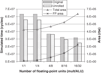
Figure 7.12 Comparison of increases in area and performance for unrolled transform stage. The maximum performance per area is achieved with eight floating-point multipliers (mult) and 16 ALUs.

This section has demonstrated that application modeling can provide useful predictions of the broad computational characteristics of a 3-D engine. While the predicted times may not be accurate due to the need for estimating instruction counts, the overall trends can usually be used as a basis for further development. The only trend not predicted by our simple analysis is the growth in rasterizer time due to increasing numbers of triangles.
7.5 APPLICATION STUDY: IMAGE COMPRESSION
A number of intraframe operations are common to both still image compression methods such as JPEG, and video compression methods such as MPEG and H.264. These include color space transformation and entropy coding (EC). Video compression methods usually also include interframe operations, such as motion compensation (MC), to take advantage of the fact that successive video frames are often similar; these will be described in Section 7.6.
7.5.1 JPEG Compression
The JPEG method involves 24 bits per pixel, eight each of red, green, and blue (RGB). It can deal with both lossy and lossless compression. There are three main steps [42].
First, color space transformation. The image is converted from RGB into a different color space such as YCbCr. The Y component represents the brightness of a pixel, while the Cb and Cr components together represent the chrominance or color. The human eye can see more detail in the Y component than in Cb and Cr, so the latter two are reduced by downsampling. The ratios at which the downsampling can be done on JPEG are 4:4:4 (no downsampling), 4:2:2 (reduce by factor of 2 in horizontal direction), and most commonly 4:2:0 (reduce by factor of 2 in horizontal and vertical directions). For the rest of the compression process, Y, Cb, and Cr are processed separately in a similar manner. These three components form the input in Figure 7.13.
Figure 7.13 Block diagram for JPEG compression. Color space transformation is not shown.

Second, discrete cosine transform (the DCT block in Figure 7.13). Each component (Y, Cb, Cr) of the image is arranged into tiles of 8 × 8 pixels each, then each tile is converted to frequency space using a two-dimensional forward DCT (DCT, type II) by multiplication with an 8 × 8 matrix. Since much information is covered by the low-frequency pixels, one could apply quantization—another matrix operation—to reduce the high-frequency components.
Third, EC. EC is a special form of lossless data compression. It involves arranging the image components in a “zigzag” order accessing low-frequency components first, employing run-length coding (RLC) algorithm to group similar frequencies together in the AC component and differential pulse code modulation (DPCM) on the DC component, and then using Huffman coding or arithmetic coding on what is left. Although arithmetic coding tends to produce better results, the decoding process is more complex.
As an example for estimating the amount of operations, consider a 2-D DCT involving k × k blocks. We need to compute:
![]()
for 0 < i ≤ k, input x, DCT coefficients c, and output y. We would need k image data loads, k coefficient data loads, k multiply accumulations, and 1 data store. So in total there are 3k + 1 operations/pixel. Hence each k × k block DCT with row–column decomposition has 2k2 (3k + 1) operations.
For frames of n × n resolution at f fps, the number of operations is 2fn(3k + 1). Two common formats are CIF (Common Intermediate Format) and QCIF (Quarter CIF), which correspond, respectively, to a resolution of 352 × 288 pixels and 176 × 144 pixels.
For a YCbCr QCIF frame with 4:2:0 sampling ratio, which has 594 tiles of 8 × 8 blocks, at 15 fps the total number of operations is: 2 × 15 × 594 × 8 × 8 × (24 + 1) = 28.5 million operations per second (MOPS). For a CIF frame, 114 MOPS are required.
Typically, lossless compression can achieve up to three times reduction in size, while lossy compression can achieve up to 25 times reduction.
7.5.2 Example JPEG System for Digital Still Camera
A typical imaging pipeline for a still image camera is shown in Figure 7.14 [128]. The TMS320C549 processor, receiving 16 × 16 blocks of pixels from SDRAM, implements this imaging pipeline.
Figure 7.14 Block diagram for a still image camera [128]. A/D: analog to digital conversion; CFA: color filter array.

Since the TMS320C549 has 32K of 16-bit RAM and 16K of 16-bit ROM, all imaging pipeline operations can be executed on chip since only a small 16 × 16 block of the image is used. In this way, the processing time is kept short, because there is no need for slow external memory.
This device offers performance up to 100 MIPS, with low power consumption in the region of 0.45 mA/MIPS. Table 7.4 illustrates a detailed cycle count for the different stages of the imaging pipeline software. The entire imaging pipeline, including JPEG, takes about 150 cycles/pixel, or about 150 instructions/pixel given a device of 100 MIPS at 100 MHz.
TABLE 7.4 TMS320C54X Performance [128]
| Task | Cycles/Pixel |
| Preprocessing: for example, gain, white balancing | 22 |
| Color space conversion | 10 |
| Interpolation | 41 |
| Edge enhancement, false color suppression | 27 |
| 4:1:1 decimation, JPEG encoding | 62 |
| Total | 152 |
A TMS320C54x processor at 100 MHz can process 1 megapixel CCD (charge coupled devices) image in 1.5 second. This processor supports a 2 second shot-to-shot delay, including data movement from external memory to on-chip memory. Digital cameras should also allow users to display the captured images on the LCD screen on the camera, or on an external TV monitor. Since the captured images are stored on a flash memory card, playback-mode software is also needed on this SOC.
If the images are stored as JPEG bitstreams, the playback-mode software would decode them, scale the decoded images to appropriate spatial resolutions, and display them on the LCD screen and/or the external TV monitor. The TMS320C54x playback-mode software can execute 100 cycles/pixel to support a 1 second playback of a megapixel image.
This processor requires 1.7 KB for program memory and 4.6 KB for data memory to support the imaging pipeline and compress the image according to the JPEG standard. The complete imaging pipeline software is stored on-chip, which reduces external memory accesses and allows the use of slower external memory. This organization not just improves performance, but it also lowers the system cost and enhances power efficiency.
More recent chips for use in digital cameras would need to support, in addition to image compression, also video compression, audio processing, and wireless communication [217]. Figure 7.15 shows some of the key elements in such a chip.
Figure 7.15 Block diagram for a camera chip with video, audio, and networking capabilities.

7.6 APPLICATION STUDY: VIDEO COMPRESSION
Table 7.5 summarizes the common video formats used in various applications, together with the associated compression methods such as MPEG1, MPEG2, and MPEG4. Video quality depends on the bitrate and the video resolution—higher bitrate and higher resolution generally mean better video quality, but requiring higher bandwidth.
TABLE 7.5 Some Common Video Formats
From http://www.videohelp.com/svcd.

*Approximate resolution, can be higher or lower.
†Approximate bitrate, can be higher or lower.
Kbps, thousand bits per second; Mbps, million bits per second; min, minutes.
There is another set of compression methods known as H.261, H.262, H.363, and H.264; some of these are related to the MPEG methods, for instance MPEG2 and H.262 are the same and H.264 corresponds to MPEG4/Part 10. Generally the more recent methods such as H.264 offer higher quality and higher compression ratio. In the following we shall provide an overview of some of these video compression methods [42, 270], without going into the details.
7.6.1 MPEG and H.26X Video Compression: Requirements
In addition to intraframe compression methods for still images described earlier, video compression methods also deploy interframe compression methods such as motion estimation. Motion estimation is one of the most demanding operations in standard-based video coding, as shown in the requirement below for H.261 involving CIF images with 352 × 288 pixels at 30 fps:
968 MOPS for compression:
| RGB to YCbCr | 27 |
| Motion estimation | 608 (25 searches in 16 × 16 region) |
| Inter/intraframe coding | 40 |
| Loop filtering | 55 |
| Pixel prediction | 18 |
| 2-D DCT | 60 |
| Quant., zigzag scanning | 44 |
| EC | 17 |
| Frame reconstruct | 99 |
Most compression standards involve asymmetric computations, such that decompression is usually much less demanding than compression. For instance, for H.261, the amount of operations for decompression (around 200 MOPS) is around 20% of that for compression (about 1000 MOPS):
198 MOPS for decompression:
| Entropy decode | 17 |
| Inverse quantization | 9 |
| Inverse DCT (IDCT) | 60 |
| Loop filter | 55 |
| Prediction | 30 |
| YCbCr to RGB | 27 |
The motion estimation method involves three kinds of frames (Figure 7.16). First, the intrapicture I, which does not include motion information, so it is like lossy JPEG. Second, the picture P, which covers motion prediction based on earlier I frames; it contains motion vectors (MVs) and error terms. Since error terms are small, quantizing gives good compression. Third, the bidirectional picture B, which supports motion prediction based on past and future I or P frames.
Figure 7.16 Three kinds of frames in MPEG motion estimation.

The goal of the motion estimator is to describe the information in the current frame based on information in its reference frame. The reference frame is typically the reconstructed version of the immediately preceding frame in the sequence, which is known to both the encoder and decoder.
In the motion estimator for video compression methods such as H.264, pixel values are examined between these pairs of frames. Based on the operations of the motion estimator, the pixel values in the current frame can be alternately represented by a combination of two quantities: pixel values from a predictor based on the reference frame plus a prediction error that represents the difference between the predictor values and the actual pixel values in the current frame.
The function of the motion estimator can be interpreted in the following way. Suppose that the image of a moving object is represented by a group of pixels in the current frame of the original video sequence, as well as by a group of pixels in the previous frame of the reconstructed sequence. The reconstructed sequence is the designated reference frame. To achieve compression, the pixel representation of the object in the current frame is deduced from the pixel values in the reference frame. The pixel values representing the object in the reference frame is called the predictor, because it predicts the object’s pixel values in the current frame. Some changes are usually needed in the predictor to attain the true pixel values of the object in the current frame; these differences are known as the prediction error.
In block-based motion estimation, the boundaries of objects represented in the current frame are assumed to approximately align along the boundaries of macroblocks. Based on this assumption, objects depicted in the frame can be represented well by one or more macroblocks. All pixels within a macroblock share the same motion characteristics. These motion characteristics are described by the macroblock’s MV, which is a vector that points from the pixel location of the macroblock in the current frame to the pixel location of its predictor. Video coding standards do not dictate how the MV and prediction error are obtained.
Figure 7.17 illustrates the process of motion estimation. Typically, the motion estimator examines only the luminance portion of the frame, so each macroblock corresponds to 16 × 16 luminance pixels. The current frame is subdivided into nonoverlapping macroblocks. To each macroblock, the motion estimator assigns a predictor, which must necessarily also be a square region of the size of 16 × 16 luminance pixels. The predictor can also be considered a macroblock. It is chosen based on the “similarity” between it and the macroblock in the current frame.
Figure 7.17 Motion estimation process.

The similarity metric for the macroblocks is not specified by video coding standards such as H.264; a commonly used one is the SAD (sum of the absolute difference) metric, which computes the SAD between the values of corresponding luminance pixels in two macroblocks.
All macroblocks in a search region of the reference frame are evaluated against the current macroblock using the SAD metric. A larger SAD value indicates a greater difference between two macroblocks. The predictor macroblock is chosen to be the one which has the lowest SAD.
Many video compression standards require the search region to be rectangular and located about the coordinates of the original macroblock. The dimensions of the rectangle are adjustable but may not exceed a standard-specified maximum value.
The search strategy used to find the best-matching predictor macroblock, called the motion search, is usually not specified by the standard. Many motion search algorithms have been proposed. One possible motion search is an exhaustive (or full) search over all possible macroblocks in the search region; this strategy guarantees a global SAD minimum within the search region. However, exhaustive search is computationally expensive and is therefore primarily adopted by hardware designers, due to its regularity.
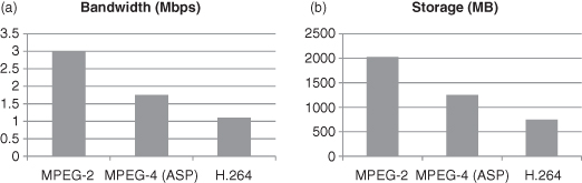
Figure 7.18 summarizes bandwidth and storage requirements of different compression methods for 90 minutes of DVD-quality video.
Figure 7.18 Bandwidth (a) and storage (b) of different video compression methods. ASP stands for Active Simple Profile, a version of MPEG-4.
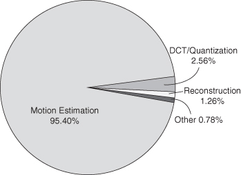
If we look at the percentage execution time of the operations in a compression or a decompression algorithm, it can be seen that motion compensation and motion estimation usually take the lion’s share. For instance, H.264/AVC (Advanced Video Coding) decompression contains four major kernels: motion compensation, integer transform, entropy coding, and deblocking filtering. Motion compensation is the most time-consuming module; see Figure 7.19.
Figure 7.19 Comparing kernels in H.264/AVC decompression.

Similar results have been reported for compression as well. For instance, Figure 7.20 shows that motion estimation can take over 95% of execution time in a software H.263 encoder [270].
Figure 7.20 Comparing kernels in H.263 compression with a basic encoder using half-pel exhaustive motion search [270].
7.6.2 H.264 Acceleration: Designs
One of the most common digital video formats is H.264. It is an international standard that has been adopted by many broadcasting and mobile communication standards, such as DVB and 3G. Its coding efficiency has enabled new applications for streaming video.
Advanced algorithms are included in H.264 for motion estimation and for other methods for video compression. For motion estimation, blocks from 16 × 16 to 4 × 4 pixels are supported. Residual data transforms are applied to 4 × 4 blocks with modified integer DCT to prevent rounding errors.
H.264 provides better results than previous standards, due to the adoption of wider search ranges, multiple reference frames, and smaller macroblocks for motion estimation and motion compensation—at the expense of increased load in computation. It requires, for example, high-speed memory and highly pipelined designs, to meet the demand of various encoding tasks, such as those in motion estimation.
Let us consider two approaches. The first approach is to implement the tasks in programmable or dedicated hardware. For instance, a recent design of a baseline H.264/AVC encoder core [158] has been implemented in various hardware technologies, including:
1. 4CIF (704 × 576) at 30 fps with low-cost FPGAs: Xilinx Spartan-3 and Altera Cyclone-II,
2. 720 pixels (1280 × 720) at 30 fps with high-end FPGAs: Xilinx Virtex-4 and Altera Stratix-II,
3. 1080 pixels (1920 × 1080) at 30 fps with 0.13-µm ASIC.
The features of these implementations are summarized in Table 7.6.
TABLE 7.6 FPGA and ASIC Designs for H.264/AVC Encoding [158]

ALUT, Adaptive Lookup Table; M4K, a configurable memory block with a total of 4,608 bits.
The second approach is to implement the tasks on a software configurable processor introduced in Section 6.5.3, which has an instruction set extension fabric (ISEF) to support demanding operations implemented as custom instructions (also called extension instructions). The one used here is a 300-MHz Stretch S5 processor, which achieves H.264 encoding of Standard Definition (SD) video at 30 fps [152]. We shall look at this approach in more detail below.
Successful real-time video encoding applications have to deliver the best image quality feasible for a particular screen resolution, given real-world operating constraints. For example, an uncompressed video stream has an image size of 720 × 480 pixels and requires 1.5 bytes for color per pixel. Such a stream has 518 KB per frame, and at 30 fps it consumes 15.5 MB per second storage and bandwidth.
Figure 7.21 shows the architecture of an H.264 encoder. The efficiency of the encoder can be found in the implementation of the following functions:
1. forward DCT and IDCT,
2. intraprediction utilizing forward and inverse quantization,
3. deblocking filtering, and
4. motion estimation employing interframe comparisons.
Figure 7.21 H.264 encoder architecture [152]. ME, motion estimation; MC, motion compensation; Quant, quantization.
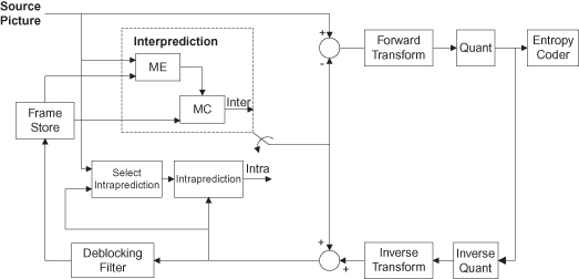
The above are prime candidates for hardware acceleration because of the amount of computation required. Additional acceleration can be achieved by taking advantage of the inherent parallelism in these algorithms.
DCT
Consider the processing of 4 × 4 blocks of luma pixels through a 2-D DCT and quantization step. The computations for the DCT portion of the matrix computation can be reduced to 64 add and subtract operations by taking advantage of symmetry and common subexpressions. All 64 operations can be combined into a single custom instruction for the ISEF.
Quantization (Q)
This follows the DCT. The division operation, which is costly, is avoided by implementing quantization as a simple multiply and shift operation. Total processing required for luma encode and decode using DCT + Q + IDCT + IQ involves about 594 additions, 16 multiplications, and 288 decisions (using multiplexers).
Deblocking Filtering
The 128-bit bus to the ISEF takes a single cycle to load a row of eight 16-bit prediction data. So one ISEF instruction can replace many conventional instructions, provided that the compiler can recognize the inherent parallelism in the function. The total number of cycles to perform these operations on a 4 × 4 block using a standard processor is over 1000 cycles. The same processing can be done in the software configurable processor in 105 cycles, offering more than 10 times acceleration. Hence a video stream of 720 × 480 pixels at 30 fps would only require 14.2% utilization of the RISC processor, since the bulk of the task is off-loaded to the ISEF. Increasing sub-block sizes enhances parallelism: for example, operating on two 4 × 4 blocks in parallel reduces execution time in half, dropping the utilization of the RISC processor to 7.1% as the ISEF takes on a heavier load.
Accelerating deblocking requires developers to minimize conditional code. Instead of determining which values to calculate, it is often more efficient to create a single custom instruction that calculates all the results in hardware and then select the appropriate result.
Reordering the 128-bit result from the IDCT stage simplifies packing of 16 8-bit edge data pixels into a single 128-bit wide datum to feed the deblocking custom instruction. Precalculating macroblock parameters is another optimization option supported by the state registers inside the ISEF and the instruction.
The filter’s inner loop loads the 128-bit register and executes the deblockFilter() custom instruction, computing two edges per instruction. Because the same custom instruction can be used for both horizontal and vertical filtering, there is zero overhead.
This inner loop takes three cycles and is executed twice (horizontal and vertical), with about 20 cycles for loop overhead. With 64 edges in each MB of data, there are approximately 416 (64/4 × 26) cycles required per MB. For a video stream of resolution 720 × 480 pixels at 30 fps, this results in 16.8 Mcycles/s, or approximately 5.2% processor utilization.
Motion Estimation
This is known to consume much of the processor budget (50–60%). The key computation requirements are the repeated SAD calculations used in determining the best MV match.
The data calculations and comparisons are repetitive, with many of the intermediate results needing to be reused. These large data sets do not fit well within the limited register space of the traditional processor and digital signal processor (DSP) architectures. Also, these processors and DSP implementations struggle to feed the fixed arithmetic and multiplier units from the data cache.
With the Stretch S5 Software Configurable Processor, the ISEF custom processing unit is capable of performing computations in parallel and holding the intermediate results in the state registers while executing fully pipelined SAD instructions.
Motion estimation consists of potentially 41 SAD and 41 MVs calculations per macroblock. A full motion search on a single macroblock requires 262K operations for a video stream at 30 fps, for a total of 10.6 giga operations per second (GOPS).
By using heuristic algorithms for many implementations, the application developer can minimize the computations to meet target image quality and/or bitrate requirements.
Custom algorithms optimized to perform estimates across different search areas, numbers of frames, or the number of MVs needing to be calculated can easily be converted to ISEF instructions. A single custom instruction can replace multiple computations, as well as pipeline many of the computations using intermediate results.
For example, a single custom instruction can perform 64 SAD calculations. The ISEF maintains the 64 partial sums to reduce the number of data transfers and to reuse the results in the next instruction. The ISEF instructions can be pipelined to improve compute capacity.
Motion estimation also involves various pixel predictions that require nine SADs computed in nine directions around the pixel. By using custom instructions, a 16 × 16 SAD calculation with quarter pixel precision takes 133 cycles, and a 4 × 4 SAD calculation with quarter pixel precision takes 50 cycles.
The above discussion covers the Stretch S5 processor. The Stretch S6 processor comes with a programmable accelerator that supports a dedicated hardware block for motion estimation, so there is no need to implement this operation in the ISEF for the S6 processor.
7.7 FURTHER APPLICATION STUDIES
This section covers a number of applications to illustrate the variety of requirements and SOC solutions.
7.7.1 MP3 Audio Decoding
MP3, short for MPEC-1/2 Audio layer-3, is probably the most popular format for high-quality compressed audio. In this section we outline the basic algorithm [42] and describe two implementations: one in ASIC, the other in an FPGA [117].
Requirements
The MPEG-1 standard involves compressing digital video and audio at a combined bitrate of 1.5 Mbps. The standard is divided into a few parts, with Part 3 dealing with audio compression. The audio compression standard contains three layers according to different levels of complexity and performance; the Layer 3 standard—commonly referred to as MP3—performs best but is also the most complex.
The MP3 audio algorithm involves perceptual encoding; a block diagram is shown in Figure 7.22. The algorithm is based on associating a psychoacoustic model to a hybrid sub-band/transform coding scheme. The audio signal is divided into 32 sub-band signals, and a modified discrete cosine transform (MDCT) is applied to each sub-band signal. The transform coefficients are encoded according to a psychoacoustically motivated perceptual error measure, using scalar quantization and variable-length Huffman coding.
Figure 7.22 Block diagram for perceptual encoding and decoding [42].

The MP3 bitstream is a concatenation of sequence of data “frames,” where each frame corresponds to two “granules” of audio such that each granule is defined as precisely 576 consecutive audio samples. A granule may sometimes be divided into three shorter ones of 192 samples each.
There are three main steps involved in decoding an MP3 frame. First, synchronize to the start of the frame and decode header information. Second, decode the side information including scale factor selection information, block splitting information, and table selection information. Third, decode the main data for both granules, including the Huffman bits for the transform coefficients, and scale factors. The main data may overflow into adjoining frames, so multiple frames of data may need to be buffered.
After the frame bits have been parsed, the next stage is to reconstruct the audio for each granule from the decoded bits; the following steps are involved:
1. Dequantizing the transform coefficients from the main and side information. A nonlinear transformation is applied to the decoded coefficients.
2. In the case of short blocks, the dequantized coefficients may be reordered and divided into three sets of coefficients, one per block.
3. In the case of certain stereo signals where the right (R) and left (L) channels may be jointly encoded, the transform coefficients are recast into L and R channel coefficients via a channel transformation.
4. An “alias reduction” step is applied for long blocks.
5. The inverse MDCT (IMDCT) module is applied for coefficients corresponding to each of the 32 sub-bands in each channel.
6. An overlap-add mechanism is used on the IMDCT outputs generated in consecutive frames. Specifically, the first half of the IMDCT outputs arc overlapped and added with the second half of the IMDCT outputs generated in the corresponding sub-band in the previous granule.
7. The final step is performed by an inverse polyphase filterbank for combining the 32 sub-band signals back into a full-bandwidth, time-domain signal.
Design
Function-level profiling for an ARM processor and a DSP processor reveals that the synthesis filter bank is the most time-consuming task (Table 7.7).
TABLE 7.7 MP3 Profiling Results for ARM and DSP Processors
| Module | Percentage Time on ARM | Percentage Time on DSP |
| Header, side intonnation, decoding scale factors | 7 | 13 |
| Huffman decode, stereo processing | 10 | 30 |
| Alias reduction, IMDCT | 18 | 15 |
| Synthesis filter bank | 65 | 42 |
An ASIC prototype has been fabricated in a five metal layer 350 nm CMOS process from AMI Semiconductor [117]. The chip contains five RAMs including the main memory, and a ROM for the Huffman tables (Table 7.8). The core size is approximately 13 mm2. The power consumption is 40 mW at 2 V and 12 MHz. It is possible to lower the clock frequency to 4–6 MHz while still complying with the real-time constraints.
TABLE 7.8 MP3 Decoding Blocks in 350-nm ASIC Technology [117]

The real-time requirement for the decoding process is determined by the audio information in an MP3 frame. Table 7.9 presents the computation time for the different sub-blocks for a 24 MHz system clock [117]. The total time for the decoding process is 2.3 ms, which results in a slack of 24.7 ms. This shows that the clock speed for the decoder can be reduced, and that resources can be shared to lower costs.
TABLE 7.9 Resource Utilization and Computation Time for MP3 Decoding Blocks in Xilinx Virtex-II 1000 FPGA Technology [117]
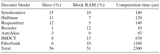
The resource utilization on a Virtex-II 1000 FPGA is also reported in Table 7.9. This design takes up 56% of the FPGA slices, 15% of the flip-flops, 45% of the four-input lookup tables, and 57% of the block RAMs. Moreover, a 32 × 32 bit multiplier, which is shared among the sub-blocks, is made from four of the available 18 × 18 bit multipliers.
As indicated above, there is scope for reducing the area and power consumption of this design by resource sharing among sub-blocks. However, such resource sharing may complicate control and implementation, for instance by introducing routing bottlenecks; hence, its pros and cons must be evaluated before adoption.
7.7.2 Software-Defined Radio with 802.16
The WiMAX or IEEE 802.16 wireless communications standard, along with a variety of other wireless communication standards, attempts to increase the data transfer rates to meet the demands for end applications and to reduce deployment costs. The techniques used to identify the digital data in the presence of large amounts of noise stress the computational capabilities of most processors. With the standards still evolving and the requirements changing, a programmable solution is particularly attractive.
Requirements
The basic transmitter block diagram for an 802.16 implementation is shown in Figure 7.23 [169]. At the high level, the physical layer (PHY) on the transmitter is responsible for converting the raw digital data stream to a complex data stream ready for upconverting to an analog radio signal. The PHY on the receiver is responsible for extracting the complex data stream and decoding the data back to the original form.
Figure 7.23 802.16 transmitter block diagram [169] IP stack, internet protocol stack; ARQ, automatic repeat reQuest; IFFT, inverse FFT; LPF, low-pass filter; PAPR, peak to average power ratio; RF, radio frequency.

The blocks in PHY that are computationally demanding include fast Fourier transforms (FFT) and its inverse, forward error correction (FEC) including block coding such as Reed–Solomon codec and bit-level coding such as convolution encoding and Viterbi decoding, quadrature amplitude modulation (QAM), interleaving, and scrambling. The media access control (MAC) layer provides the interface between the PHY and the network layer. The MAC processing is much more control oriented as it takes packets from the network layer and schedules the data to be sent according to the quality of service (QoS) requirements; while at the receiver end, the MAC reassembles the data for handing back to the network layer. The MAC layer also includes the necessary messaging to maintain communications between the base and the subscriber stations as well as automatically requesting the retransmission of any bad packets. The network layer is the interface to the application. A TCP/IP network stack is the most common networking stack in use today. For a complete wireless solution, all layers must be connected.
Design
The physical layer PHY in the 802.16 WiMAX standard performs 256-point FFT and orthogonal frequency-division multiplexing (OFDM). On a Stretch S5 Software Configurable Processor (Section 6.5.3), the OFDM can be configured to operate in channel widths of 3.5, 7, and 10 MHz [169]. Modulation support includes BPSK (Binary Phase Shift Keying), QPSK (Quadrature Phase Shift Keying), 16 QAM or 64 QAM. For noisy environments, the FEC is a requirement, with the standard allowing a variety of choices. Note that a conventional RISC or DSP processor does not have enough power to support the high demand of WiMAX baseband processing and the control tasks at the same time. A single software configurable processor meets the demand of all the heavy-duty WiMax signal processing and control tasks such as a base MAC layer and full TCP/IP stack to achieve full bitrate for all three channel widths on a single chip.
The Stretch Software Configurable Processor adopts a Radix-2 FFT design through defining a custom instruction as an extension instruction, which supports sixteen 16 × 16 multiplies, eight 32-bit adds, and sixteen 16-bit adds with rounding and rescaling operation. This custom instruction makes use of the 128-bit wide registers to pass three sets of four complex values to the ISEF for parallel operations. This results in performing 256-point FFT in 4 µs. Implementing a Radix-4 FFT provides an additional 28% performance improvement.
The FEC block is another one that benefits from flexibility and performance. Forward error correction increases data throughput in the presence of channel noise by introducing data redundancy on the transmitter side, and errors are corrected on the receiver side. In convolutional coding, every encoded bit is generated by convolving the input bit with the previous input bits. The constraint length is the number of bits used in the computation and the rate is the number of input bits per output bit. The WiMax standard uses convolutional encoding with the constraint length of 7 and a rate of 1/2. Other rates can also be supported.
RISC processors are often not sufficiently efficient for the bit-level operations involved in convolutional encoding. In the Stretch Software Configurable Processor, bit-level operations can be optimized by making use of the custom processing unit ISEF. A custom instruction is implemented to take 64 bits from the input to generate 128 outputs. This custom instruction uses internal states to keep six state bits; it performs parallel processing of 64 input bits by convolving the input bits with the state bits to produce 128 outputs.
The bitstreams generated by convolutional encoding can be decoded by using a trellis diagram to find the most likely sequence of codes. A Viterbi decoder is an efficient way to decode the bitstream by limiting the number of sequences needed to be examined. It keeps a record of the most likely path for each state at each trellis stage. Viterbi decoding is computationally demanding; it requires add–compare–selection (ACS) for each state at each stage, as well as keeping the history of the selected path. It involves three main steps: (1) branch metric computation, (2) ACS for each state at each stage, and (3) traceback.
In the trellis diagram, there is a metric associated with each branch, called branch metric, which measures the distance between a received signal and the output branch labels. Branch metric is computed as the Euclidean distance between the received sample and branch label.
One custom instruction, EI_ACS64, is created to perform the branch metric computation, addition of the branch metric with the path metric at the previous stage, comparing the path metrics of the two incoming paths, and updating the path metric with the maximum and then selecting the path. This EI_ACS64 instruction does this ACS operation for all the states at one trellis stage in parallel. In other words, this custom instruction performs 32 butterfly operations in parallel. The 64 path metrics are stored as internal states in ISEF. As we move from one stage to the next stage, EI_ACS64 also updates output wide registers with 1 bit for each state, which indicates the selected path. As we traverse four trellis stages, it will accumulate 4 bits for each state. In total, it accumulates 4 × 64 = 256 bits for all the states. Two store instructions (WRAS128IU) can then be used to move these bits to memory.
The actual decoding of symbols back to the original data is accomplished by tracing backwards through the trellis along the maximum likelihood path. The length of the traceback is commonly four to five times the constraint length of the convolutional encoder. In some cases, the entire frame of data is received before beginning traceback. We traverse the trellis in reverse direction to decode the input bitstream. Assume the state reached at the last trellis stage is in a known state, typically state 0. This can be achieved by sending additional K − 1 bits of 0 to bring all the states to 0. The bit stored for each state tells which branch to traverse as we traverse from stage j to j − 1. Another custom instruction is created, VITERBI_TB, which does traceback for four trellis stages, uses an internal state to keep the previous state for the next round of traceback, and outputs 4 bits for the decoded bitstream. The VITERBI_TB instruction is called twice before the 8-bit decoded bitstream is stored back to memory.
7.8 CONCLUSIONS
We hope that the material in this chapter has illustrated the variety of SOC applications and the range of design techniques and SOC architectures—ranging from embedded ARM processors to reconfigurable devices from Xilinx and Stretch—many of which have been introduced in the preceding chapters. Interestingly, the rapid increase in performance requirements in multimedia, cryptography, communications, and other key applications has led to a wave of start-ups, such as Achronix, Element CXI, Silicon Hive, Stretch, and Tabula; time will tell which are the winners.
We have not, however, attempted to provide a detailed and complete account of design development for a specific application or design style using the latest tools. Such accounts are already available: for instance, Fisher et al [93] and Rowen and Leibson [207] have dedicated their treatment, respectively, to VLIW architectures and to configurable processors. SOC design examples [164] and methodologies [32] from an industrial perspective are also available. Those interested in detailed examples involving application of analytical techniques to processor design are referred to the textbooks by Flynn [96] and by Hennessy and Patterson [118].
7.9 PROBLEM SET
1. How fast would a 32-bit processor with the ARM7 instruction set need to run to be able to support AES for Wi-Fi 802.11b? How about a 64-bit processor?
2. Estimate the number of operations per second involved in computing the DCT for high-resolution images of 1920 × 1080 pixels at 30 fps.
3. Explain how the JPEG system for the camera in Figure 7.14 can be revised to support 10 megapixel images.
4. Estimate the size in number of rbes of the FPGA and ASIC designs in Table 7.6, assuming that the FPGAs are produced in a 90 nm process.
5. Compare the pros and cons of the FPGA and ASIC designs in Table 7.6, assuming that the FPGAs are produced in a 90 nm process. How would your answer change when both the FPGAs and the ASIC are produced in a 45 nm process?
6. Consider a 3-D graphics application designed to deal with k nonclipped triangles, each covering an average of p pixels and a fraction α of which being obscured by other triangles. Ambient and diffuse illumination models and Gouraud shading are used. The display has a resolution of m × n pixels, updated at f fps. Estimate:
(a) the number of floating-point operations for geometry operations,
(b) the number of integer operations for computing pixel values, and
(c) the number of memory access for rasterization.
7. Table 7.10 shows data for the ARM1136J-S PXP system. The datapath runs at a maximum of 350 MHz for the 16K instruction cache plus 16K data cache; the 32K + 32K and 64K + 64K implementations are limited in speed by their cache implementations.
(a) Comment on the effect of increasing the size of L1 on performance.
(b) Suggest reasons to explain why the design with the largest cache area is not the fastest.
(c) Compare the fastest design and the one just behind that one. Which one is more cost effective and why?
TABLE 7.10 MPEG4 Decode Performance on ARM1136J-S PXP System

Area values include that of L2 where appropriate.
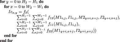
8. Figure 7.24 shows a convolution algorithm between an H1 × W1 image (I1) and an H2 × W2 image (I2), which have optional masks M1 and M2, respectively, of the same width and height. Given that H2 > H1 and W2 > W1, and f3, f12, f11, and f22 are pure functions—that is, they have no internal state and their results depend only on their parameters:
(a) What are the values of M1, M2 and f3, f12, f11, and f22 for (1) SAD correlation, (2) normalized correlation, and (3) Gaussian blur?
(b) What is the resolution of the result image Ic?
(c) How many cycles are needed to produce the resulting image Ic?
Figure 7.24 Convolution algorithm with resulting image Ic.