
6
Customization and Configurability
6.1 INTRODUCTION
To broaden SOC applicability while reducing cost, one can adopt a common hardware platform that can be customized to improve efficiency for specific applications. This chapter looks at different customization technologies, particularly those based on configurability. Here configurability covers both one-time configurability, when application-oriented customization takes place once either before or after chip fabrication, and reconfigurability, when customization takes place multiple times after chip fabrication.
Customization opportunities at design time, particularly those exploited in device fabrication, often result in high performance but at the expense of flexibility when the design is deployed. Such postfabrication flexibility is achieved by devices with various degrees of programmability, including coarse-grained reconfigurable architectures (CGRAs), application-specific instruction processors (ASIPs), fine-grained field-programmable gate arrays (FPGAs), digital signal processors (DSPs), and general-purpose processors (GPPs). The trade-off between programmability and performance is shown in Figure 6.1, which is introduced in Chapter 1.
Figure 6.1 A simplified comparison of different technologies: programmability versus performance. GPP stands for general-purpose processor, while CGRA stands for coarse-grained reconfigurable architecture.

Structured ASIC (application-specific integrated circuit) technology supports limited customization before fabrication compared with custom ASIC technology. In Figure 6.1, the ASIPs are assumed to be customized at fabrication in ASIC technology. ASIPs can also be customized at compile time if implemented in FPGA technology as a soft processor; a customizable ASIP processor will be presented in Section 6.8.
There are many ways of customizing SOC designs, and this chapter focuses on three of them:
1. customization of instruction processors (Sections 6.4 and 6.8), illustrating how (a) availability of processor families and (b) generation of application-specific processors can offer architectural optimizations such as very long instruction word (VLIW), vectorization, fused operation, and multithreading to meet requirements in performance, area, energy efficiency, and costs;
2. customization of reconfigurable fabrics (Sections 6.5 and 6.6), showing that fine-grained reconfigurable functional units (FUs) and the related interconnect resources are versatile but incur large overheads—hence coarse-grained blocks are increasingly adopted to reduce such overheads;
3. customization techniques for optimizing implementations, such as instance-specific design (Section 6.7) and run-time reconfiguration strategies (Section 6.9), together with methods for assessing related trade-offs in performance, size, power, and energy efficiency.
Other customization methods, such as those based on multiprocessors, would not be treated in detail. Pointers to references on various related topics are included in Section 6.10.
6.2 ESTIMATING EFFECTIVENESS OF CUSTOMIZATION
It is important to be able to estimate and compare the effectiveness of different ways of customization applied to part of a design. The method is simple. For a given metric such as delay, area, or power consumption, assume that α is the factor of improvement applicable to a fraction β of a design. So the metric is improved by:
![]()
This metric is reminiscent of the parallel processor analysis of G. Amdahl. As an example, consider the well-known 90:10 rule: a good candidate for acceleration is the case when 10% of the code takes 90% of the time. What happens if that 10% of the code can be accelerated k times?
From the expression above with α = 1/k, β = 0.9, we obtain (k + 9)/10k. Assuming k = 10, the execution time is reduced to 19% of the original, resulting in a speedup of 5.26 times.
However, if the effect of the code that can be accelerated is reduced from 90% of the time to only 60% of the time, we can find that the speedup is only 2.17 times—almost halved.
Note that the amount of code, which provides an estimate of the amount of effort required for customizing it, does not affect the above result; it is the effect of the customizable fraction on the metric that matters, not the fraction itself.
This method can be applied in various ways. As another example, consider the use of embedded coarse-grained blocks to customize a fine-grained reconfigurable fabric, as we shall explain in a later section. Assume that 50% of the fine-grained fabric can be replaced by coarse-grained blocks, which are three times more efficient in speed and 35 times more efficient in area. One can find that the design could be improved up to 50% faster with its area reduced by half.
There are, however, several reasons against customizability. Tools for customizable processors such as performance profilers and optimizers are often not as mature as those for noncustomizable processors; backwards compatibility and verification can also become an issue. One approach is to develop customizable processors that are compatible with existing noncustomizable building blocks, such that there is interoperability between customizable and noncustomizable technologies [94].
6.3 SOC CUSTOMIZATION: AN OVERVIEW
Customization is the process of optimizing a design to meet application requirements and implementation constraints. It can take place at design time and at run time. Design time has two components: fabrication time and compile time. During fabrication time, a physical device is constructed. If this device is configurable, then after fabrication it can be customized by a program produced at compile time and executed at run time.
There are three common means of implementing computations: standard instruction processors, ASICs, and reconfigurable devices.
1. For standard instruction processors such as those from ARM, AMD, and Intel, fabrication-time customization produces a device supporting a fixed instruction set architecture, and compile-time customization produces instructions for that architecture; run-time customization corresponds to locating or generating appropriate code for execution at run time.
2. For ASICs, much of the customization to perform application functions takes place at fabrication time. Hence the high efficiency but low flexibility, since new functions not planned before fabrication cannot easily be added. Structured ASICs, such as gate array or standard-cell technologies, reduce design effort by limiting the options of customization to the user to, for instance, the metal layers. One-time customization of antifuse technology can be performed in the field.
3. Reconfigurable devices generally include FPGA and complex programmable logic device (CPLD) technology, as well as instruction processors coupled with a reconfigurable fabric to support custom instructions [25]. In this case, fabrication-time customization produces a device with a reconfigurable fabric, typically containing reconfigurable elements joined together by reconfigurable interconnections. At compile time, configuration information is produced from a design description for customizing the device at appropriate instants at run time.
The standard instruction processors are general purpose. There are, however, opportunities to customize the instruction set and the architecture for a specific application. For instance, the standard instruction set can be customized to remove unused instructions or to include new instructions that would result in improved performance. Custom instruction processors can be customized during fabrication in ASIC technology or during configuration in reconfigurable hardware technology.
- Processors that are customized during fabrication include those from ARC and Tensilica. Typically some of the building blocks are hardwired at fabrication to support, for instance, domain-specific optimizations, including instructions that are customized for specific applications. To reduce risk, there are often reconfigurable prototypes before designs are implemented in ASIC technology.
- For soft processors such as MicroBlaze [259] from Xilinx or Nios [11] from Altera, the challenge is to support instruction processors efficiently using resources in a reconfigurable fabric such as an FPGA. Efficiency can be improved by exploiting device-specific features or run-time reconfigurability [213].
- Another alternative is to implement the instruction processor in ASIC technology, and a suitable interface is developed to enable the processor to benefit from custom instructions implemented in a reconfigurable fabric. An example is the software configurable processor from Stretch [25], which consists of the Xtensa instruction processor from Tensilica and a coarse-grained reconfigurable fabric. These devices can offer higher efficiency than FPGAs when an application requires resources that match their architecture.
A key consideration for deciding which technology to use is volume. Recall from Chapter 1 that the product cost usually has a fixed or nonrecurring component that is independent of volume and has a variable or recurrent component that varies with volume. Reconfigurable technologies like FPGAs have little fixed cost, but have a higher unit cost than ASIC technologies. Hence, below a certain volume threshold, reconfigurable technologies offer the lowest cost—and this threshold moves in favor of reconfigurable technologies with time, since the cost of mask sets and other fixed fabrication costs increase rapidly with each new generation of technology.
There are various ways of classifying a customizable SOC. A customizable SOC typically consists of one or more processors, reconfigurable fabrics, and memories. One way is to classify such SOCs according to the coupling between the reconfigurable fabric and the processor [61].
Figure 6.2a shows the reconfigurable fabric attached to the system bus. Figure 6.2b illustrates the situation when the reconfigurable fabric is a coprocessor of the CPU, with a closer coupling between them than the ones in Figure 6.2a.
Figure 6.2 Four classes of customizable SOC [61; 244]. The shaded box denotes the reconfigurable fabric. (a) Attached processing unit; (b) coprocessor; (c) reconfigurable FU; (d) processor embedded in a reconfigurable fabric.

Next, Figure 6.2c shows an architecture in which the processor and the fabric are tightly coupled. In this case, the reconfigurable fabric is part of the processor itself, perhaps forming a reconfigurable subunit that supports custom instructions. An example of this organization is the software configurable processor from Stretch.
Figure 6.2d shows another organization. In this case, the processor is embedded in the programmable fabric. The processor can either be a “hard” core [261] or can be a “soft” core, which is implemented using the resources of the reconfigurable fabric itself; examples include the MicroBlaze and the Nios processors mentioned earlier.
It is also possible to integrate configurable analog and digital functionality on the same chip. For instance, the PSoC (programmable system on a chip) device [68] from Cypress has an array of analog blocks that can be configured as various combinations of comparators, filters, and analog-to-digital converters, with programmable interconnects. The inputs and outputs of these and the reconfigurable digital blocks can be flexibly routed to the input/output (I/O) pins. Moreover, these blocks can be reconfigured to perform different functions when the system is operating.
6.4 CUSTOMIZING INSTRUCTION PROCESSORS
Microprocessors in desktop machines are designed for general-purpose computation. Instruction processors in an SOC are often specialized for particular types of computations such as media processing or data encryption. Hence they can benefit from customization that is highly specific to their intended function, eliminating hardware elements that would not be needed. Such customization usually takes place before fabrication, although many techniques can also be applied to the design of soft processors. Customization allows designers to optimize their designs to meet requirements such as those in speed, area, power consumption, and accuracy, while improving product differentiation.
6.4.1 Processor Customization Approaches
There are two main approaches for providing customized processors. The first approach is to provide families of processors customized for specific application domains. For example, ARM provides the Cortex-A Series for supporting applications with demanding computation, the Cortex-R Series for real-time processing, the Cortex-M series for microcontrollers in embedded applications (with the Cortex-M1 processors optimized for FPGA implementation), and the SecurCore processors for tamper-resistant smart cards. Each series contains a range of processors with different characteristics, allowing designers to choose one that best fits their requirements in function and performance, including power and energy consumption.
The second approach is to provide the capability of generating customized processors. Companies such as ARC and Tensilica provide design tools to allow SOC designers to configure and extend a processor, either through a graphical user interface or through tools based on an architecture description language. Such tools enable designers to add only the features they need while deleting the features they do not need. In addition, they allow designers to extend the architecture of the core by adding custom instructions, allowing further optimization of the processor for the end application.
To help optimize the design for size, power, and application performance, some SOC tools provide guidelines for final silicon area and memory requirements. Designers are able to configure features around the core, such as the type and size of caches, interrupts, DSP subsystem, timers, and debug components, as well as features within the core, such as the type and size of core registers, address widths, and instruction set options. The aim is to support rapid performance and die-size trade-offs to provide an optimized solution. Specific functions often included in SOC tools are:
- Integration of intellectual properties from various sources.
- Generation of simulation scripts and test benches for system verification.
- Enhancement of software development tools to support, for instance, custom instructions for the customizable processor.
- Automated generation of FPGA designs for an emulation platform.
- Documentation of selected configuration for inclusion in licensees’ chip specifications and customer-level documentation.
Such tools can usually configure and deliver a custom processor within minutes. Also, by generating all configuration-specific information required for testing, downstream development tools, and documentation, the configurator reduces time to silicon and reduces project risk.
Further information about tools and applications of customizable embedded processors can be found in various publications [127, 207].
6.4.2 Architecture Description
As processors become increasingly complex, it is useful to provide a significant degree of automation in implementing both the processor and the software tools associated with that processor. Without automation, much design and verification effort is needed to build a processor and its tools from scratch for every application.
To automate development of processors and tools, architecture description languages or processor description languages can help [179]. Such languages should be sufficiently concise and high level for designers to adopt them for different applications; they should also be comprehensive enough to produce realistic, efficient implementations. Many languages have been proposed for describing instruction processors. The goal of these languages is to capture the design of a processor so that supporting tools and the processor itself can be automatically generated.
Architecture description languages can be classified by the description style and by the level and type of automation provided. For example, one can classify architecture description languages as either behavioral, structural, or a combination of the two.
Behavioral descriptions are instruction-set centric: The designer specifies the instruction set and then uses tools to generate a compiler, assembler, linker, and simulator. The nML [87] and TIE [240] languages fall into the behavioral category. Automating generation of a compiler backend from a behavioral description is facilitated when the instructions can be expressed as a tree grammar for a code-generator-generator tool such as BURG [100]. Many behavioral languages support synthesis of processor hardware, and synthesis tools are available for the above examples. In the case of TIE, synthesis is simplified since the base processor is fixed and only extensions to this base processor can be specified by designers. The nML “Go” tool designs the processor architecture automatically [86] from the instruction set, inferring structure from explicitly shared resources such as the register file.
The main advantage of a behavioral description is the high level of abstraction: only an instruction set specification is required to generate a custom processor. The main disadvantage is the lack of flexibility in the hardware implementation. Synthesis tools must fix some aspects of the microarchitecture [87] or even the entire base processor [240]. Efficient synthesis from an instruction set alone is a difficult design automation problem when resource sharing [50] is taken into account.
Structural descriptions capture the FUs, storage resources, and interconnections of a processor. SPREE [269] is a library built onto C++ that generates FPGA soft processors using a structural description. In particular, the designer can remove instructions or change the implementation of FUs, since SPREE provides a method for connecting functional blocks, with built-in support for common functions such as forwarding networks and interlocks.
The main advantage of structural descriptions is that they can be directly converted into a form suitable for synthesis to hardware. Additionally, most structural description styles maintain the generality of a hardware description language (HDL). This generality provides much scope for describing diverse microarchitectures, for example, superscalar or multithreaded ones. The prime disadvantage is the lower level of abstraction: the designer needs to manually specify FUs and control structures.
We present a summary of existing processor description languages in Table 6.1. For each language, we indicate the description style, the scope (whole processor or just instruction set), and the tools available to automate generation of a processor system.
TABLE 6.1 Features of Some Architecture Description Languages

Some systems, such as LISA [119], cover both structural and behavioral information. This combines the advantages of pure behavioral and structural descriptions, but there is a need to ensure that related behavioral and structural elements are consistent.
All languages except TIE are whole processor descriptions, meaning that the entire processor design is specified, as opposed to just the instruction set. However, many processor description languages are specific to a particular basic processor architecture, such as in-order execution in the case of LISA and nML. Customizable threaded architecture (CUSTARD) [77], which would be covered in Section 6.8, is based on the MIPS instruction set while supporting various customization options, such as the type of multithreading and the use of custom instructions.
Possible tools for such languages include [179]:
- Model Generation. Tools for producing hardware prototypes and validation models for checking that the architecture specification captures the requirements.
- Test Generation. Tools for producing test programs, assertions, and test benches.
- Toolkit Generation. Tools for profiling, exploring, compiling, simulating, assembling, and debugging designs.
6.4.3 Identifying Custom Instructions Automatically
Various approaches have been proposed for automatic identification of instruction set extensions from high-level application descriptions. One can cluster related dataflow graph (DFG) nodes heuristically as sequential or parallel templates. Input and output constraints are imposed on the subgraphs to reduce the exponential search space.
Various architectural optimizations—some described in the earlier chapters—can benefit the automatically generated designs, such as [110]:
- VLIW techniques enable a single instruction to support multiple independent operations. A VLIW format partitions an instruction into a number of slots, each of which may contain one of a set of operations. If the instruction set is designed to use VLIW, a source language compiler can use software-pipelining and instruction-scheduling techniques to pack multiple operations into a single VLIW instruction.
- Vector operations increase throughput by creating operations that operate on more than one data element. A vector operation is characterized by the operation it performs on each data element and by the number of data elements that it operates on in parallel, that is, the vector length. For example, a four-wide vector integer addition operation sums two input vectors, each containing four integers, and produces a single result vector of four integers.
- Fused operations involve creating operations composed of several simple operations. A fused operation potentially has one or more of the input operands fixed to a constant value. Using the fused operation in place of the simple operations reduces code size and issue bandwidth, and may reduce register file port requirements. Also, the latency of the fused operation may be lower than the combined latency of the simple operations.
Application of constraint propagation techniques results in an efficient enumerative algorithm. However, the applicability of this approach is limited to DFGs with around 100 nodes. Search space can be further reduced by imposing additional constraints such as single output, or connectivity constraints on the subgraphs.
The identification of instruction set extensions under input and output constraints can be formulated as an integer linear programming problem. Biswas et al. [45] propose an extension to the Kernighan–Lin heuristic based on input and output constraints. Optimality is often limited by either an approximate search algorithm or some artificial constraints—such as I/O constraints—to make subgraph enumeration tractable.
An integer linear programming formulation can replace I/O constraints with the actual data bandwidth constraints and data transfer costs. The instruction set extensions that are generated may have an unlimited number of inputs and outputs. A baseline machine with architecturally visible state registers makes this approach feasible. Promising results are obtained by integrating the data bandwidth information directly into the optimization process, by explicitly accounting for the cost of the data transfers between the core register file and custom state registers [28].
There are many approaches in customizing instruction processors. A technology-aware approach could involve a clustering strategy to estimate the resource utilization of lookup table (LUT)-based FPGAs for specific custom instructions, without going through the entire synthesis process [148]. An application-aware approach could, in the case of video applications, exploit appropriate intermediate representations and loop parallelism [165]. A transformation-aware approach could adopt a method based on combined but phased searching of the source-level transformation design space and the instruction set extension design space [182].
6.5 RECONFIGURABLE TECHNOLOGIES
Among various technologies, FPGAs are well known. Their capacity and capability have improved rapidly in the last few years to support high-performance designs. Their low cost and support for rapid development make them ideal for designs requiring fast time to market, as well as for education and student projects.
The following covers the reconfigurable fabric that underpins FPGAs and other reconfigurable devices. The reconfigurable fabric consists of a set of reconfigurable FUs, a reconfigurable interconnect, and a flexible interface to connect the fabric to the rest of the system. We shall review each of these components and show how they have been used in both commercial and academic reconfigurable systems. The treatment here follows that of Todman et al. [244].
In each component of the fabric, there is a trade-off between flexibility and efficiency. A highly flexible fabric is typically larger and slower than a less flexible fabric. On the other hand, a more flexible fabric can better adapt to application requirements. This kind of trade-off can influence the design of reconfigurable systems. A summary of the main features of various architectures can be found in Table 6.2. There are many related devices, such as those from Elixent [82], that we are unable to include due to limited space.
TABLE 6.2 Comparison of Reconfigurable Fabrics and Devices
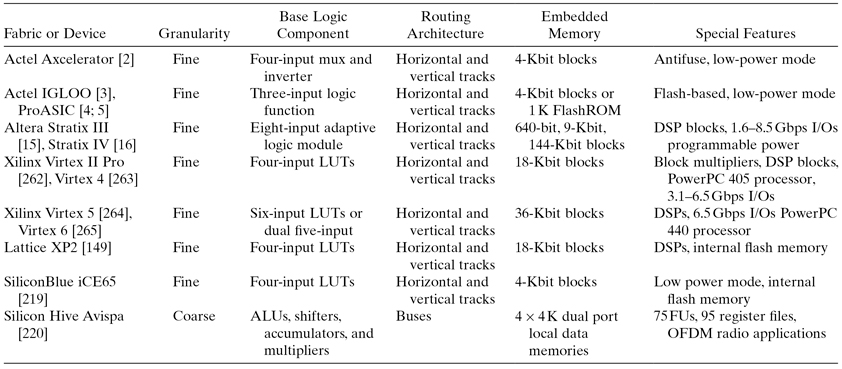
OFDM: orthogonal frequency-division multiplexing.
6.5.1 Reconfigurable Functional Units (FUs)
Reconfigurable FUs can be classified as either coarse grained or fine grained. A fine-grained FU can typically implement a single function on a single bit, or a small number of bits. The most common kind of fine-grained FUs are the small LUTs that are used to implement the bulk of the logic in a commercial FPGA. A coarse-grained FU, on the other hand, is typically much larger, and may consist of arithmetic and logic units (ALUs) and possibly even a significant amount of storage. In this section, we describe the two types of FUs in more detail.
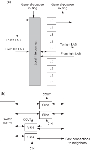
Many reconfigurable systems use commercial FPGAs as a reconfigurable fabric. These commercial FPGAs contain many three to six input LUTs, each of which can be thought of as a fine-grained FU. Figure 6.3a illustrates a LUT; by shifting in the correct pattern of bits, this FU can implement any single function of up to three inputs—the extension to LUTs with larger numbers of inputs is clear. Typically, LUTs are combined into clusters, as shown in Figure 6.3b. Figure 6.4 shows clusters in two popular FPGA families. Figure 6.4a shows a cluster in the Altera Stratix device; Altera calls these clusters “logic array blocks” (LABs) [14]. Figure 6.4b shows a cluster in the Xilinx architecture [262]; Xilinx calls these clusters “configurable logic blocks” (CLBs). In the Altera diagram, each block labeled “LE” is an LUT, while in the Xilinx diagram, each “Slice” contains two LUTs.
Figure 6.3 Fine-grained reconfigurable FUs [244]. (a) Three-input LUT; (b) cluster of LUTs.
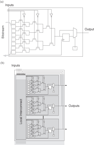
Figure 6.4 Commercial logic block architectures. (a) Altera LAB [14]; (b) Xilinx CLB [262].
Reconfigurable fabrics containing LUTs are flexible and can be used to implement any digital circuit. However, compared to the coarse-grained structures described below, these fine-grained structures have significantly more area, delay, and power overhead. Recognizing that these fabrics are often used for arithmetic purposes, FPGA companies have included additional features such as carry chains and cascade chains to reduce the overhead when implementing common arithmetic and logic functions.
While the efficiency of commercial FPGAs is improved by adding architectural support for common functions, one can go further and embed significantly larger, but less flexible, reconfigurable FUs. There are two kinds of devices that contain coarse-grained FUs.
First, many commercial FPGAs, which consist primarily of fine-grained FUs, are increasingly enhanced by the inclusion of larger blocks. For instance, the early Xilinx Virtex device contains embedded 18 × 18 bit multiplier units [262]. When implementing algorithms requiring a large amount of multiplication, these embedded units can significantly improve the density, speed, and power consumption. On the other hand, for algorithms that do not perform multiplication, these blocks are rarely useful. The Altera Stratix devices contain a larger, but more flexible embedded block, called a DSP block, which can perform accumulate functions as well as multiply operations. The comparison between the two devices clearly illustrates the flexibility and overhead trade-off: the Altera DSP block may be more flexible than the Xilinx multiplier, but it consumes more chip area and runs slower for the specific task of multiplication. Recent Xilinx devices have a more complex embedded unit, called DSP48. It should be noted that, while such embedded blocks eliminate reconfigurable interconnects within them, their fixed location can cause wiring congestion and overhead. Moreover, they would become an overhead for applications that do not make use of them.
Second, while commercial FPGAs described above contain both fine-grained and coarse-grained blocks, there are also devices that contain only coarse-grained blocks. An example of a coarse-grained architecture is the ADRES architecture, which is shown in Figure 6.5 [171]. Each reconfigurable FU in this device contains a 32-bit ALU that can be configured to implement one of several functions including addition, multiplication, and logic functions, with two small register files. Clearly, such an FU is far less flexible than the fine-grained FUs described earlier; however, if the application requires functions that match the capabilities of the ALU, these functions can be efficiently implemented in this architecture.
Figure 6.5 ADRES reconfigurable FU [171]. Pred is a one-bit control input selecting either Src1 or Src2 for the functional unit.

6.5.2 Reconfigurable Interconnects
Regardless of whether a device contains fine-grained FUs, coarse-grained FUs, or a mixture of the two, the FUs needed to be connected in a flexible way. Again, there is a trade-off between the flexibility of the interconnect (and hence the reconfigurable fabric) and the speed, area, and power efficiency of the architecture.
Reconfigurable interconnect architectures can be classified as fine grained or coarse grained. The distinction is based on the granularity with which wires are switched. This is illustrated in Figure 6.6, which shows a flexible interconnect between two buses. In the fine-grained architecture in Figure 6.6a, each wire can be switched independently, while in Figure 6.6b, the entire bus is switched as a unit. The fine-grained routing architecture in Figure 6.6a is more flexible, since not every bit needs to be routed in the same way; however, the coarse-grained architecture in Figure 6.6b contains fewer programming bits, and hence has lower overhead.
Figure 6.6 Routing architectures. (a) Fine grained; (b) coarse grained.
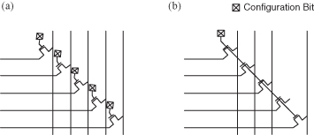
Fine-grained routing architectures are usually found in commercial FPGAs. In these devices, the FUs are typically arranged in a grid pattern and they are connected using horizontal and vertical channels. Significant research has been performed in the optimization of the topology of this interconnect [157].
Coarse-grained routing architectures are commonly used in devices containing coarse-grained FUs. Figure 6.7 shows two examples of coarse-grained routing architectures. The routing architecture in Figure 6.7a is used in the Totem reconfigurable system [60]; the interconnect is designed to be flexible and to provide arbitrary connection patterns between FUs. On the other hand, the routing architecture in Figure 6.7b, which is used in the Silicon Hive reconfigurable system, is less flexible, but faster and smaller [220]. In the Silicon Hive architecture, only connections between units that are likely to communicate are provided.
Figure 6.7 Examples of coarse-grained routing architectures. (a) Totem coarse-grained routing architecture [60]; (b) Silicon Hive coarse-grained routing architecture [220]. GPR: General Purpose Registers, MULT: Multiplier. RF: register file, LS: Load/Store Unit.

6.5.3 Software Configurable Processors
Software configurable processors are devices introduced by Stretch. They have an architecture that couples a conventional instruction processor to a reconfigurable fabric to allow application programs to dynamically customize the instruction set. Such architectures have two benefits. First, they offer significant performance gains by exploiting data parallelism, operator specialization, and deep pipelines. Second, application builders can develop their programs using the Stretch C compiler without having expertise in electronic design.
A software configurable processor consists of a conventional 32-bit RISC processor coupled with a programmable instruction set extension fabric (ISEF). There are also an ALU for arithmetic and logic operations and a floating-point unit (FPU) for floating-point operations. Figure 6.8 shows the S6 Software Configurable Processor Engine.
Figure 6.8 The Stretch S6 Software Configurable Processor Engine [230]. IRAM denotes embedded memory for the instruction set extension fabric (ISEF).
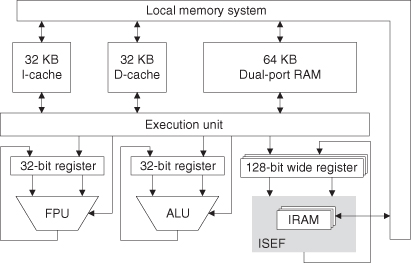
The ISEF consists of an array of blocks, each containing an array of 4-bit ALUs and an array of multiplier elements, interconnected by a programmable routing fabric. The 4-bit ALUs can be cascaded through a fast carry circuit to form up to 64-bit ALUs. Each 4-bit ALU may also implement up to four 3-input logic functions, with four register bits for extension instruction state variables or for pipelining.
The ISEF supports multiple application-specific instructions as extension instructions. Arguments to extension instructions are provided from 32 wide registers, which are 128 bits wide. Each extension instruction may read up to three 128-bit operands and write up to two 128-bit results. A rich set of dedicated load and store instructions are provided to move data between the 128-bit wide register and the 128-bit wide cache and memory subsystem. The ISEF supports deep pipelining by allowing extension instructions to be pipelined.
In addition to the load/store model, a group of extension instructions may also define arbitrary state variables to be held in registers within the ISEF. State values may be read and modified by any extension instruction in the group, thereby reducing the Wide Register traffic.
In addition to the Software Configurable Processor Engine, there is also a programmable accelerator, which consists of a list of functions implemented in dedicated hardware. These functions include motion estimation for video encoding, entropy coding for H.264 video, cryptographic operations based on Advanced Encryption Standard (AES) and Triple Data Encryption Standard (3DES) schemes, and various audio codecs including those for MP3 and AC3.
To develop an application, the programmer identifies critical sections to be accelerated, writes one or more extension instructions as functions in a variant of the C programming language called Stretch C, and accesses those functions from the application program. Further information about application mapping for software configurable processors can be found in the next section, and related application studies for the Stretch S5 Software Configurable Processor Engine can be found in Sections 7.6.2 and 7.7.2.
6.6 MAPPING DESIGNS ONTO RECONFIGURABLE DEVICES
The resources in a reconfigurable device need to be configured appropriately to implement a design for a given application. We shall look at the ways designs are mapped onto an FPGA and onto a software configurable processor.
A typical tool flow for an FPGA is shown in Figure 6.9 [56]. In the conventional tool flow, HDLs such as VHDL and Verilog are widely used to target commercial devices to describe the circuit to be implemented in the FPGA. The description of the circuit is written at the register transfer level (RTL), which specifies the operations at each clock cycle. The description is then synthesized to a netlist of logic blocks before being placed and routed for the FPGA.
Figure 6.9 Tool flow for FPGA.
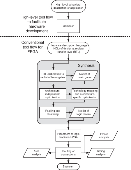
In the first stage of the synthesis process, the datapath operations in an RTL design such as control logic, memory blocks, registers, adders, and multipliers are identified and elaborated into a set of basic boolean logic gates such as AND, OR, and XOR.
Next, the netlist of basic gates is optimized independent of the FPGA architecture. The optimization includes: boolean expression minimization, removing the redundant logic, buffering sharing, retiming, and finite-state machine encoding. The optimized netlist of basic gates is then mapped to the specific FPGA architecture such as Xilinx Virtex devices or Altera Stratix devices. There is further optimization based on the specific architecture such as carry chains for adders and dedicated shift functions in logic block for shift registers. The final stage in the synthesis process is packing and clustering groups of several LUTs and registers into logic blocks like Figure 6.4. The packing and clustering minimize the number of connections between different logic blocks. After the synthesis process, the logic blocks in the mapped netlist are placed onto the FPGA based on the different optimization goals, such as circuit speed, routability, and wire length. Once the location of the logic blocks is determined, the connection between I/Os, logic blocks, and other embedded elements are routed onto the programmable routing resources in FPGA. The routing process determines which programmable switches should be used to connect the logic block input and output pins. Finally, a configuration bitstream for all inputs and outputs, logic blocks, and routing resources for the circuit in specific FPGA is generated.
The above description covers design mapping for fine-grained FPGA resources. Many reconfigurable devices also have coarse-grained resources for computation and for storage (see Section 6.5.1), so FPGA design tools need to take such resources into account.
To improve productivity, high-level programming languages are included in the tool flow for FPGAs (the upper part of Figure 6.9). These languages and tools, such as AutoPilot [272], Harmonic [159], and ROCC [248], enable application developers to produce designs without detailed knowledge of the implementation technology. Some of these compilers are able to extract parallelism in the computation from the source code, and to optimize for pipelining. Such tools often improve productivity of application developers, at the expense of the quality of the design. However, since device capacity and capability continue to increase rapidly, productivity of application developers is likely to become the highest priority.
Besides configuring the circuit, there are tools that analyze the delay, area, and power consumption of the implemented circuit. These tools are used to check whether the circuit meets the requirements of the application developer.
For a Software Configurable Processor from Stretch, the compilation needs to target both the execution unit and the ISEF shown in Figure 6.8. The first stage of the Stretch C compiler [25] takes an extension instruction and applies various optimizations, such as constant propagation, loop unrolling, and word-length optimization. In addition, sequences of operators are aggregated into balanced trees where possible; operators are specialized with multiplication by a constant converted into shifts and adds; and resources among operators for different instructions are shared. The compiler then produces two main outputs: instruction header and latency information including register usage for the Xtensa compiler, and a structured netlist of the operators extracted from the source code for mapping to the resources in the ISEF [25].
The Xtensa compiler compiles the application code with references to the extension instructions. It uses the instruction header and timing data from the Stretch C compiler to perform register allocation and optimized scheduling of the instruction stream. The result is then linked to the ISEF bitstream.
The ISEF bitstream generation stage in the Stretch compiler is similar to the tool flow for FPGAs shown earlier. The four main stages are [25]:
- Map. Performs module generation for the operators provided by the initial stage of the Stretch C compiler.
- Place. Assigns location to the modules generated by Map.
- Route. Performs detailed, timing-driven routing on the placed netlist.
- Retime. Moves registers to balance pipeline stage delays.
The linker packages the components of the application into a single executable file, which contains a directory of the ISEF configurations for the operating system or the run-time system to locate instruction groups for dynamic reconfiguration.
6.7 INSTANCE-SPECIFIC DESIGN
Instance-specific design is often used in customizing both hardware and software. The aim for instance-specific design is to optimize an implementation for a particular computation. The main benefits are improving speed and reducing resource usage, leading to lower power and energy consumption at the expense of flexibility.
We describe three techniques for automating instance-specific design. The first technique is constant folding: propagating static input values through a computation to eliminate unnecessary hardware or software. As an example, an instance-specific version of the hardware design in Figure 6.10 specialized to particular filter coefficients is shown in Figure 6.11. The improvement in efficiency is due to the fact that one-input constant-coefficient multipliers are smaller and faster than two-input multipliers.
Figure 6.10 An FIR filter containing two-input multipliers that support variable filter coefficients. The triangular blocks denote registers [197].
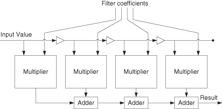
Figure 6.11 An FIR filter containing one-input constant-coefficient multipliers that support instance-specific filter coefficients [197].

The ability to implement specialized designs, while at the same time providing flexibility by allowing different specialized designs to be loaded onto a device, can allow reconfigurable logic to be more effective than ASICs in implementing some applications. For other applications, performance improvements from optimizing designs to a particular problem instance can help to shift the price/performance ratio away from ASICs and toward FPGAs.
Significant benefits for instance-specific design have been reported for a variety of applications. For FIR (Finite Impulse Response) filters, a modified common subexpression elimination algorithm can be used to reduce the number of adders used in implementing constant-coefficient multiplication [180]. Up to 50% reduction in the number of FPGA slices and up to 75% reduction in the number of LUTs for fully parallel implementations have been observed, in comparison to designs based on distributed arithmetic. Moreover, there is up to 50% reduction in the total dynamic power consumption of the FIR filters.
Changing an instance-specific design at run time is usually much slower than changing the inputs of a general circuit, since a new full or partial configuration must be loaded, which may take many tens or hundreds of milliseconds. It is therefore important to carefully choose how a design is specialized. Related discussions on run-time reconfiguration can be found in Section 6.9.
The second technique for automating instance-specific design is function adaptation, which involves changing a function in hardware or software to achieve, for a specific application instance, the desired trade-off in the performance or resource usage of the function and the quality of the result produced by the function.
An example of function adaptation is word-length optimization. Given the flexibility of fine-grain FPGA, it is desirable to automate the process of finding a good custom data representation. An important implementation decision to automate is the selection of an appropriate word length and scaling for each signal in a DSP system. Unlike microprocessor-based implementations where the word length is defined a priori by the hard-wired architecture of the processor, reconfigurable computing based on FPGAs allows the size of each variable to be customized to produce the best trade-offs in numerical accuracy, design size, speed, and power consumption.
The third technique for automating instance-specific design is architecture adaptation, which involves changing the hardware and software architecture to optimize for a specific application instance, such as supporting relevant custom instructions. We shall discuss this technique in more detail in the next section.
An illustration of the above three techniques is given in Table 6.3. Further information about instance-specific design can be found elsewhere [197].
TABLE 6.3 Some Illustrations of Instance-Specific Design

6.8 CUSTOMIZABLE SOFT PROCESSOR: AN EXAMPLE
This section describes a multithreaded soft processor called CUSTARD with a customizable instruction set [77]. It illustrates the material from the preceding sections: we show how an instruction processor can be customized by adapting the architecture to support different types of multithreading and custom instructions; we then present the associated tool flow targeting reconfigurable technology.
CUSTARD supports multiple contexts within the same processor hardware. A context is the state of a thread of execution, specifically the state of the registers, stack, and program counter. Supporting threads at the hardware level brings two significant benefits. First, a context switch—changing the active thread—can be accomplished within a single cycle, enabling a uniprocessor to interleave execution of independent threads with little or no overhead. Second, a context switch can be used to hide latency where a single thread would otherwise busy-wait.
The major cost of supporting multiple threads stems from the additional register files required for each context. Fortunately, current FPGAs are rich in on-chip block memories that could be used to implement large register files. Additional logic complexity must also be added to the control of the processor and the current thread must be recorded at each pipeline stage. However, the bulk of the pipeline and the FUs are effectively shared between multiple threads, so we would expect a significant area reduction over a multiprocessor configuration.
Instances of CUSTARD processors are generated using a parameterizable model. The key elements of this parameterizable model are shown in Figure 6.12. This model is used both in instantiating a synthesizable hardware description and in configuring a cycle-accurate simulator.
Figure 6.12 CUSTARD microarchitecture showing threading, register file, and forwarding network parameterizations.
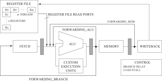
The CUSTARD base architecture is typical of a soft processor, with a fully bypassed and interlocked 4-stage pipeline. It is a load/store RISC architecture supporting the MIPS integer instruction set. It is also capable of augmenting the pipeline with custom instructions using spare portions of the MIPS opcode space.
There are four sets of parameters for customizing CUSTARD. The first set covers multithreading support: one can specify the number of threads and the threading type, either block multithreading (BMT) or interleaved multithreading (IMT). The second set covers custom instructions and the associated datapaths at the execution stage of the pipeline as well as custom memory blocks. The third set covers the forwarding and interlock architecture: whether the Branch delay slot, the Load delay slot, and the forwarding paths are necessary. The fourth set covers the register file: the number of registers and the number of register file ports.
Two types of multithreading, BMT and IMT, are supported. Both types simultaneously maintain the context—the state of registers, program counter, and so on—of multiple independent threads. The types of threading differ in the circumstances that context switches are triggered.
BMT triggers a context switch as a result of some run-time event in the currently active thread, for example, a cache miss, an explicit “yield” of control, or the start of some long latency operation such as a custom instruction. When only a single thread is available, the BMT processor behaves exactly as a conventional single-threaded processor. When multiple threads are available, any latency in the active thread is hidden by a context switch. The context switch is triggered at the execution stage of the pipeline, such that the last instruction fetched must be flushed and refilled from the new active thread.
IMT performs a mandatory context switch every single cycle, resulting in interleaved execution of the available threads. IMT permits simplification of the processor pipeline since, given sufficient threads, certain pipeline stages are guaranteed to contain independent instructions. IMT thus removes pipeline hazards and permits simplification of the forwarding and interlock network designed to mitigate these hazards. The CUSTARD processor can exploit this capability by selectively removing forwarding paths to optimize the processor for a particular threading configuration.
Table 6.4 summarizes the customization of the forwarding and interlock architecture for each multithreading configuration. The forwarding paths, BRANCH, ALU, and MEM, are illustrated in Figure 6.12. The IMT columns show how elements of the forwarding and interlock network can be removed depending upon the number of available threads. For example, in the case of two threads, the ALU forwarding logic can be removed. When two IMT threads are available, any instruction entering the ALU stage of the pipeline is independent of the instruction leaving the ALU stage. Removing interlocks in situations highlighted by “*” constrains the ordering of the input instructions; the relevant parameters are made available to the compiler, which can then adapt the scheduling of instructions.
TABLE 6.4 Summary of Forwarding Paths (As Shown in Figure 5.12) and Interlocks That Can Be “Optimized Away” for Single-Threaded, Block Multithreaded (BMT), and Interleaved Multithreaded (IMT) Parameterizations
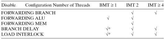
*Optimizing away this element in this configuration changes the compiler scheduler behavior to prevent hazards.
Multiple contexts are supported by multiple register files that are implemented as dual-port RAM on the FPGA. Each register file access is indexed by the register number and also the ID of the thread that generated the access. Each register file is also parameterizable in terms of the number of ports and the number of registers per thread. Increasing the number of register file ports allows custom instructions to be selected by the compiler that take a greater number of operands.
An approach based on compiling a parallel imperative language into hardware [191] is used to implement the parameterizable processor. This implementation of CUSTARD provides a framework for parameterization of the processor together with a route to hardware. The associated compiler outputs MIPS integer instructions and custom instructions to optimize CUSTARD for a given application; Table 6.5 shows the custom instructions for some benchmarks.
TABLE 6.5 A Summary of the Custom Instructions Automatically Generated for a Set of Benchmarks

Inputs r0 − r3 are allocated to registers from the general purpose file. LUT(a) = table lookup from dedicated block RAM (BRAM) address a. “Num. Uses” demonstrates the extent of reuse by showing the number of times the instruction is used in the benchmark assembly code. Latency is the number of execution cycles required before the output is available to the forwarding network or in the register file.
Figure 6.13 shows the flow through the CUSTARD tools. Custom instructions are generated based on a technique known as similar sub-instructions [77]. Prior to finding custom instructions, a preoptimization stage performs standard source-level optimizations together with loop unrolling to expose loop parallelism. After custom instructions have been selected, custom and base instructions are scheduled to minimize pipeline stalls. This scheduling stage is parameterizable to support the microarchitectural changes afforded by the CUSTARD multithreading modes.
Figure 6.13 Tool flow for the CUSTARD processor customized for a particular application.

The result of compilation comprises hardware datapaths to implement custom instructions and software to execute on the customized processor. Custom instruction datapaths are added to the CUSTARD processor, and the decoding logic is revised to map new instructions to unused portions of the opcode space.
There is a cycle-accurate simulator based upon the SimpleScalar framework [30]. The simulator can be configured directly from the processor hardware description and simulates a parameterizable memory system.
Five benchmarks—Blowfish, Colourspace, AES, discrete cosine transform (DCT), and SUSAN—have been developed for a CUSTARD processor implemented on a Xilinx XC2V2000 FPGA. It is found that the IMT4 (IMT with four threads) and BMT4 (BMT with four threads) configurations add only 28% and 40% area, respectively, to the single-threaded processor, while allowing interleaved execution of four threads with no software overhead. Moreover, custom instructions give a significant performance increase, an average of 72% with a small area overhead above the same configuration without custom instructions, an average of only 3%. CUSTARD accelerates AES by 355%.
The IMT processors without custom instructions provide a higher maximum clock rate than both BMT (41% higher) and single-threaded (5% higher) processors. The number of cycles is also reduced by an average of 10%. The IMT processors hide pipeline latencies by tightly interleaving independent threads. We anticipate that the relatively low (10%) improvement is caused by the short latency of the custom instructions generated (Table 6.5), at most two cycles in every case. It is not possible to build longer latency instructions within the register file port constraints, so we expect that deeply pipelined processors or floating point custom instructions are needed to create latencies long enough for significant benefit in this area. However, the IMT processors allow a higher maximum clock rate by removing the forwarding logic around the ALU. The ALU forwarding logic is necessarily on the critical path in the BMT and single-threaded processors, as indicated by the timing analyzer reports.
6.9 RECONFIGURATION
There are many motivations for reconfiguration. One motivation is to share resources that are not required concurrently. Another motivation is to upgrade to support new functions, new standards, or new protocols. A third reason is to adapt the hardware based on run-time conditions.
Run-time reconfiguration has shown promise for many applications, including automotive systems [35], high-performance computing [81], interconnection networks [161], video processing [211], and adaptive Viterbi decoding [241]. The treatment below abstracts from the specific technology, focusing on overhead analysis of designs involving run-time reconfiguration.
6.9.1 Reconfiguration Overhead Analysis
Adapting an architecture to specific applications aims to improve performance by applying application-specific optimizations. However the performance gained by adaptation has to outweigh the cost of reconfiguration. Consider a software function f() that takes tsi time to execute on an architecture with a standard, general-purpose instruction set. When adapted to support a custom instruction, it takes tci time to execute, and can be expressed as a fraction of the original execution time as αtsi, where 0 < α < 1. The device on which f() executes requires tr time to reconfigure. We define a reconfiguration ratio R that helps us decide if reconfiguration to this new architecture is desirable by analyzing the overhead involved:
The reconfiguration ratio R gives us a measure of the benefits of reconfiguring to the new adapted architecture; R provides the improvement factor of the new implementation after reconfiguration, over the current implementation. The point where R = 1 is the threshold: if R > 1, reconfiguration will be beneficial. It is, however, important to note that an R value of 2 does not necessarily translate to an overall twofold system performance increase. The maximum reconfiguration ratio Rmax is a measure of the absolute performance gain, discounting reconfiguration time. It is the maximum possible R value for a custom instruction. This is determined as follows:
(6.2)
![]()
The maximum potential reconfiguration ratio Rpot is a measure of the maximum rate at which performance improvement is possible; it gives an idea of how quickly a custom instruction will cross the reconfiguration threshold:
(6.3)
![]()
Rpot provides an indication on the granularity of reconfiguration and size of functions that will benefit from adaptation. A function with a higher Rpot value can be adapted more easily. It can be shown that:
(6.4)
![]()
Hence an Rpot of 5 means that the custom instruction produced need only be four-fifths the speed of the original software version, before it becomes worth implementing. An Rpot of 4 requires the custom instruction to be three-fourths the speed of the original, while an Rpot of 3, two-thirds the speed of the original, and so on.
If function f() has an Rpot value of 1, the adaptation and subsequent reconfiguration of that function will not be beneficial.
The reconfiguration ratio can also be described in terms of the number of clock cycles of an FIP. Consider a software function f(), which takes tsi units of time to execute. The function takes nsi clock cycles to execute, and the cycle time is Tsi. The function f() is called F times over the period we are investigating, in this case one execution of the application. Similarly with tci:
The reconfiguration time tr can be rewritten as the product of the reconfiguration cycle time Tr and the number of configuration cycles nr. The reconfiguration cycle time, Tr, is platform dependent and is independent of the cycle time of designs implemented on the programmable device. The number of configuration cycles models the time required for either full or partial reconfiguration. In full reconfiguration, nr is a constant associated with a particular programmable device; in partial reconfiguration, nr varies with the amount of changes in the configuration. nr may also be reduced through improvements in technology and architectures that support fast reconfiguration through caches or context switches. There is a factor τ that represents certain reconfiguration overheads, such as stopping of the device prior to reconfiguration and starting of the device after reconfiguration:
In modern programmable devices, the time taken to start and stop a device can often be ignored. For instance, in Xilinx Virtex devices, this value can be as small as 10% of the time required to reconfigure a frame, the smallest atomic reconfigurable unit.
Other overheads include the time taken to save and restore the state of the processor. In the most extreme case, the state of the processor includes all storage components in the processor, for instance the register file, pipeline registers, program counter, or cache. By reinstating the state of a processor, a processor can be put back into the condition it was in when the state was saved.
After substituting Equations 6.5 and 6.6 into Equation 6.1, the reconfiguration ratio R becomes:
This equation can be used to produce a graph showing how R changes with increasing F, the number of times that the function f() is called. When R > 1, then reconfiguration is profitable. More information about this approach can be found in a description of the adaptive flexible instruction processor [213].
6.9.2 Trade-Off Analysis: Reconfigurable Parallelism
In the following we describe a simple analytical model [37] for devices that are partially reconfigurable: the larger the configured area, the longer the configuration time. For applications involving repeated independent processing of the same task on units of data that can be supplied sequentially or concurrently, increasing parallelism reduces processing time but increases configuration time. The model below would help identify the optimal trade-off: the amount of parallelism that would result in the fastest overall combination of processing time and configuration time.
The three implementation attributes are performance, area, and storage: processing time tp for one unit of data, with area A, configuration time tr, and configuration storage size Ψ. There are s processing steps, and the amount of parallelism is P.
We can also identify parameters of the application: the required data throughput is ϕapp, while there are n units of data n processed between successive configurations. The reconfigurable device has available area Amax. The data throughput of the configuration interface is ϕconfig.
Designs on volatile FPGAs require external storage for the initial configuration bitstream. Designs using partial run-time reconfiguration also need additional storage for the precompiled configuration bitstreams of the reconfigurable modules. Given A denotes the size of a reconfigurable module in FPGA tiles (e.g., CLBs) and Θ denotes a device-specific parameter that specifies the number of bytes required to configure one tile, the partial bitstream size and storage requirement Ψ (in bytes) of a reconfigurable module is directly related to its area A:
(6.8)
![]()
where h denotes the header of configuration bitstreams. In most cases, this can be neglected because the header size is very small.
The time overhead of run-time reconfiguration can consist of multiple components, such as scheduling, context save and restore, as well as the configuration process itself. In our case there is no scheduling overhead as modules are loaded directly as needed. There is also no context that needs to be saved or restored since signal processing components do not contain a meaningful state once a dataset has passed through. The reconfiguration time is proportional to the size of the partial bitstream and can be calculated as follows:
ϕconfig is the configuration data rate and measured in bytes per second. This parameter not only depends on the native speed of the configuration interface but also on the configuration controller and the data rate of the memory where the configuration data are stored.
We can distinguish between run-time reconfigurable scenarios where data do not have to be buffered during reconfiguration and scenarios where data buffering is needed during reconfiguration. For the latter case we can calculate the buffer size B depending on reconfiguration time tr and the application data throughput ϕapp:
Table 6.6 outlines the buffer size for several receiver functions and a range of reconfiguration times. We can observe that the data rate is reduced through all stages of the receiver. Hence, a reconfiguration-during-call scenario becomes easier to implement toward the end of the receiver chain. Obviously, the buffer size also increases with the bandwidth of the communication standard and the duration of the reconfiguration time.
TABLE 6.6 Buffer Size for Various Functions and Reconfiguration Times
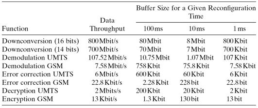
UMTS: Universal Mobile Telecommunications System, GSM: Global System for Mobile Communications
A buffer can be implemented with on-chip or off-chip resources. Most modern FPGAs provide fast, embedded RAM blocks that can be used to implement first in–first out buffers. For example, Xilinx Virtex-5 FPGAs contain between 1 and 10 Mbit of RAM blocks. Larger buffers have to be realized with off-chip memories.
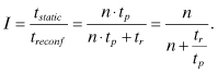
The performance of a run-time reconfigurable system is dictated by the reconfiguration downtime. If reconfigurable hardware is used as an accelerator for software functions, overall performance is usually improved despite the configuration overhead. In our case, we use reconfiguration to support multiple hardware functions in order to improve flexibility and reduce area requirements. In this case, the reconfigurable version of a design will have a performance penalty over a design that does not use reconfiguration. The reconfiguration of hardware usually takes much longer than a context switch on a processor. This is due to the relatively large amount of configuration data that need to be loaded into the device. The efficiency I of a reconfigurable design compared to a static design can be expressed as:
(6.11)
The reconfigurable system becomes more efficient by processing more data between configurations and by improving the ratio of configuration time to processing time. We propose a more detailed analysis where we consider the effect of parallelism on processing time and configuration time. Many applications can be scaled between a small and slow serial implementation, and a large and fast parallel or pipelined implementation. FIR filter, AES encryption, or CORDIC (COordinate Rotation DIgital Computer) are examples of such algorithms.
Figure 6.14 illustrates the different spatial and temporal mappings of an algorithm with regard to processing time, area, and reconfiguration time. The processing time per datum tp is inversely proportional to the degree of parallelism P. It can be calculated based on tp,e, the basic processing time of one processing element, s, the number of steps or iterations in the algorithm, and P, the degree of parallelism:
Figure 6.14 Different spatial and temporal mappings of an algorithm with s = 4 steps.
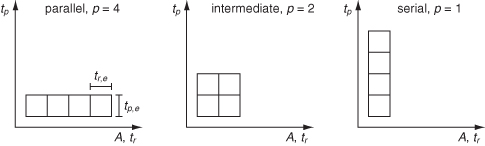
Parallelism speeds up the processing of data but slows down reconfiguration. This is because a parallel implementation is larger than a sequential one, and the reconfiguration time is directly proportional to the area as shown in Equation 6.9. The reconfiguration time tr is directly proportional to the degree of parallelism P, where tr,e is the basic reconfiguration time for one processing element:
We can now calculate the total processing time for a workload of n data items:
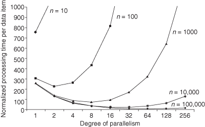
Figure 6.15 illustrates how parallelism can affect the optimality of the processing time. We consider an algorithm with s = 256 steps, which is inspired by the observation that filters can have orders of 200 or higher. The plots are normalized to processing time per datum and we assume that the reconfiguration time tr,e of one processing element is 5000 times the processing time tp,e of one processing element. This value can vary depending on the application and target device but we estimate that at least the order of magnitude is realistic for current devices. We can observe that fully sequential implementations are beneficial for small workloads. In this case, the short configuration time outweighs the longer processing time. However, the overall time is still high due to the large influence of the configuration time. Large workloads benefit from a fully parallel implementation since the processing time is more dominant than reconfiguration time. In case of medium workloads, the degree of parallelism can be tuned to optimize the processing time.
Figure 6.15 Normalized processing times for a range of workload sizes n and different levels of parallelism p. The number of steps s is set to 256 and we assume tr,e = 5000tp,e.
In order to find the optimal degree of parallelism, we calculate the partial derivative of the function given in Equation 6.14 with respect to P:
To find the minimum, we set Equation 6.15 to 0 and solve for P:

The result popt is usually a real number, which is not a feasible value to specify parallelism. In order to determine a practical value for P, popt can be interpreted according to Table 6.7.
TABLE 6.7 Interpretation of popt to Determine a Practical Value for p
| 0 < popt ≤ 1 | Fully serial implementation, p = 1 |
| 1 < popt < s | Choose P such that s/P∈Z and |popt − p| minimal |
| S ≤ popt | Fully parallel implementation, p = s |
After determining the optimal degree of parallelism that reduces the overall processing time per workload and hence maximizes performance, it is still necessary to check if the implementation meets the throughput requirements of the application Φapp:
The resulting area requirement A also has to be feasible within the total available area Amax. In summary, to implement an optimized design according to our model, the following steps have to be carried out:
1. Derive Φapp, s and n from application.
2. Obtain Φconfig for target technology.
3. Develop one design and determine tp and A.
4. Calculate tr, tp,e, and tr,e using Equations 6.9, 6.12, and 6.13.
5. Find popt from Equation 6.16 and find a feasible value according to Table 6.7.
6. Calculate ttotal using Equation 6.14 and verify throughput using Equation 6.17.
7. Implement design with P from step 5 and verify if its actual throughput satisfies the requirement.
8. Calculate buffer size B using Equation 6.10 and check A ≤ Amax.
The above methodology can be adopted for a wide variety of applications and target technologies; it will find the highest performing version of the design. In order to find the smallest design that satisfies a given throughput requirement, one can try smaller values for P while checking Equation 6.17.
This approach can also be extended to address energy efficiency for reconfigurable designs [38]; a reconfigurable FIR filter is shown to be up to 49% more energy efficient and up to 87% more area efficient than a nonreconfigurable design.
6.10 CONCLUSIONS
Customization techniques can be applied in various ways to ASIC and to configurable technologies. We provide an overview of such techniques and show how instance-specific designs and custom instruction processors can exploit customizability.
As technology advances, two effects become increasingly prominent:
1. integrated-circuit mask costs grow rapidly, making ASIC less affordable,
2. complexity of SOC design and verification keeps rising.
The technologies discussed in this chapter address these issues directly: various degrees of prefabrication customization reduce both the need for ASIC technology and the design complexity. Reconfigurable technologies such as FPGAs offer significant flexibility in the form of postfabrication customization, at the expense of overheads in speed, area, and power consumption.
Customization and configurability, in addition to their widespread adoption in commercial systems, also constitute exciting research areas, with recent progress in SOC design reuse [215], synthesizable datapath fabric [253], dynamically extensible microprocessors [48], customizable multiprocessors [90], and many others. Moreover, dynamically reconfigurable processors are beginning to be adopted commercially, such as the D-Fabrix from Panasonic, DRP-1 from NEC Electronics, and FE-GA from Hitachi [17]. It is also reported [74] that ARM processor and interconnect technologies, including ARM cell libraries and AMBA interconnect technology, would be adopted and optimized for Xilinx FPGA architectures. There is little doubt that customization and configurability will continue to play an important part in electronic systems for many years to come.
6.11 PROBLEM SET
1. Provide examples for several application domains that would benefit from postfabrication customization.
2. Some reconfigurable devices support pipelined interconnects. What are the pros and cons of pipelined interconnects?
3. Some FPGA companies provide a way of producing a structured ASIC implementation of an FPGA design, effectively removing the reconfigurability. Why do they do that?
4. Early FPGAs contain just a homogeneous array of fine-grained logic cells, while more recent ones are more heterogeneous; in addition to the fine-grained cells, they also contain configurable memory blocks, multiplier arrays, and even processor cores. Explain this evolution of FPGA architectures.
5. A subset of the instructions for a machine M can be accelerated by n times using a coprocessor C.
(a) A program P is compiled into instructions of M such that a fraction k belongs to this subset. What is the overall speedup that can be achieved using C with M?
(b) The coprocessor C in part (a) above costs j times as much as M. Calculate the minimum fraction of instructions for a program that C has to accelerate, so that the combined system of M and C is j times faster than M.
(c) The performance of M is improving by m times per month. How many months will pass before M alone, without the coprocessor C, can execute the program P in part (a) as fast as the current combined system of M and C?
6. Explain how Equation 6.7 can be generalized to cover m custom instructions.
7. A database search engine makes use of run-time reconfiguration of the hash functions to reduce the amount of processing resources. The search engine contains P processors operating in parallel; each processor can be reconfigured to implement one of h hash functions. The total number of words, w, in the input dataset is divided into ![]() subsets of words; each subset is processed using a particular hash function with one bit per word used to indicate whether a match has occurred. The indicator bit is stored along with the corresponding word in temporary memory, and such temporary data are processed by the next hash function in the processor after reconfiguration. The match indicator bit is updated in each iteration and the process continues until the data have been processed by all h hash functions. Let Th denote the critical path delay of the hash function processor, and Tr is the time for reconfiguring the processor to support a different hash function. It takes m cycles to access the memory, and the average number of characters per word is c. Consider the worst case that all the hash functions are required all the time—the analysis will become more complex if it is possible to abort the matching process if a match does not occur.
subsets of words; each subset is processed using a particular hash function with one bit per word used to indicate whether a match has occurred. The indicator bit is stored along with the corresponding word in temporary memory, and such temporary data are processed by the next hash function in the processor after reconfiguration. The match indicator bit is updated in each iteration and the process continues until the data have been processed by all h hash functions. Let Th denote the critical path delay of the hash function processor, and Tr is the time for reconfiguring the processor to support a different hash function. It takes m cycles to access the memory, and the average number of characters per word is c. Consider the worst case that all the hash functions are required all the time—the analysis will become more complex if it is possible to abort the matching process if a match does not occur.
(a) How long does it take to process one subset of data?
(b) How long does it take to process all the data?
(c) Given that each character contains b bits, how many bits are required for the temporary storage?
8. To assess the effect of reconfiguration overheads on energy efficiency, consider developing an analytical model in the same spirit as the one in Section 6.9.2, involving an application with:
- n, the number of packets or data items processed between two successive reconfigurations,
- s, the number of processing steps in the algorithm.
A reconfigurable implementation is characterized by the following parameters:
- A, the area requirement of the implementation,
- P, the amount of parallelism in the implementation,
- tp, the processing time for one packet or datum,
- tr, the reconfiguration time,
- Pp, the power consumed during processing,
- Pc, the computation power which is a component of Pp,
- Po, the power overhead which is a component of Pp,
- Pr, the power consumed during reconfiguration.
The reconfigurable device is characterized by:
- ϕconfig, the data throughput of the configuration interface,
- Θ, the configuration size per resource or unit of area.
Recall that energy is the product of power consumption and the associated time duration.
Given power consumption for computation, Pc, is directly proportional to P, the degree of parallelism, and there is a constant power consumption overhead, Po, and a constant power consumption for reconfiguration, Pr:
(a) What is the computation energy Ec for processing n data items?
(b) What is the energy overhead Eo due to Po?
(c) What is the energy for reconfiguration Er, given that the reconfiguration time is directly proportional to P?
(d) What is the total energy per data item involved in computation and reconfiguration?
(e) Find the optimal degree of parallelism that minimizes the energy per datum.