
1
Introduction to the Systems Approach
1.1 SYSTEM ARCHITECTURE: AN OVERVIEW
The past 40 years have seen amazing advances in silicon technology and resulting increases in transistor density and performance. In 1966, Fairchild Semiconductor [84] introduced a quad two input NAND gate with about 10 transistors on a die. In 2008, the Intel quad-core Itanium processor has 2 billion transistors [226]. Figures 1.1 and 1.2 show the unrelenting advance in improving transistor density and the corresponding decrease in device cost.
Figure 1.1 The increasing transistor density on a silicon die.

Figure 1.2 The decrease of transistor cost over the years.

The aim of this book is to present an approach for computer system design that exploits this enormous transistor density. In part, this is a direct extension of studies in computer architecture and design. However, it is also a study of system architecture and design.
About 50 years ago, a seminal text, Systems Engineering—An Introduction to the Design of Large-Scale Systems [111], appeared. As the authors, H.H. Goode and R.E. Machol, pointed out, the system’s view of engineering was created by a need to deal with complexity. As then, our ability to deal with complex design problems is greatly enhanced by computer-based tools.
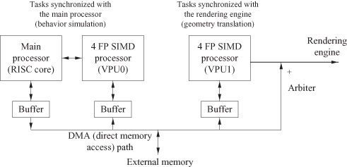
A system-on-chip (SOC) architecture is an ensemble of processors, memories, and interconnects tailored to an application domain. A simple example of such an architecture is the Emotion Engine [147, 187, 237] for the Sony PlayStation 2 (Figure 1.3), which has two main functions: behavior simulation and geometry translation. This system contains three essential components: a main processor of the reduced instruction set computer (RISC) style [118] and two vector processing units, VPU0 and VPU1, each of which contains four parallel processors of the single instruction, multiple data (SIMD) stream style [97]. We provide a brief overview of these components and our overall approach in the next few sections.
Figure 1.3 High-level functional view of a system-on-chip: the Emotion Engine of the Sony PlayStation 2 [147, 187].
While the focus of the book is on the system, in order to understand the system, one must first understand the components. So, before returning to the issue of system architecture later in this chapter, we review the components that make up the system.
1.2 COMPONENTS OF THE SYSTEM: PROCESSORS, MEMORIES, AND INTERCONNECTS
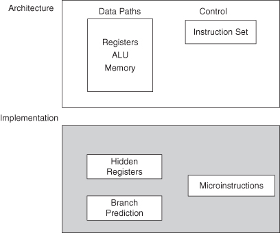
The term architecture denotes the operational structure and the user’s view of the system. Over time, it has evolved to include both the functional specification and the hardware implementation. The system architecture defines the system-level building blocks, such as processors and memories, and the interconnection between them. The processor architecture determines the processor’s instruction set, the associated programming model, its detailed implementation, which may include hidden registers, branch prediction circuits and specific details concerning the ALU (arithmetic logic unit). The implementation of a processor is also known as microarchitecture (Figure 1.4).
Figure 1.4 The processor architecture and its implementation.
The system designer has a programmer’s or user’s view of the system components, the system view of memory, the variety of specialized processors, and their interconnection. The next sections cover basic components: the processor architecture, the memory, and the bus or interconnect architecture.
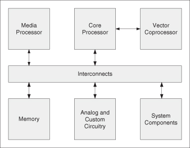
Figure 1.5 illustrates some of the basic elements of an SOC system. These include a number of heterogeneous processors interconnected to one or more memory elements with possibly an array of reconfigurable logic. Frequently, the SOC also has analog circuitry for managing sensor data and analog-to-digital conversion, or to support wireless data transmission.
Figure 1.5 A basic SOC system model.
As an example, an SOC for a smart phone would need to support, in addition to audio input and output capabilities for a traditional phone, Internet access functions and multimedia facilities for video communication, document processing, and entertainment such as games and movies. A possible configuration for the elements in Figure 1.5 would have the core processor being implemented by several ARM Cortex-A9 processors for application processing, and the media processor being implemented by a Mali-400MP graphics processor and a Mali-VE video engine. The system components and custom circuitry would interface with peripherals such as the camera, the screen, and the wireless communication unit. The elements would be connected together by AXI (Advanced eXtensible Interface) interconnects.
If all the elements cannot be contained on a single chip, the implementation is probably best referred to as a system on a board, but often is still called a SOC. What distinguishes a system on a board (or chip) from the conventional general-purpose computer plus memory on a board is the specific nature of the design target. The application is assumed to be known and specified so that the elements of the system can be selected, sized, and evaluated during the design process. The emphasis on selecting, parameterizing, and configuring system components tailored to a target application distinguishes a system architect from a computer architect.
In this chapter, we primarily look at the higher-level definition of the processor—the programmer’s view or the instruction set architecture (ISA), the basics of the processor microarchitecture, memory hierarchies, and the interconnection structure. In later chapters, we shall study in more detail the implementation issues for these elements.
1.3 HARDWARE AND SOFTWARE: PROGRAMMABILITY VERSUS PERFORMANCE
A fundamental decision in SOC design is to choose which components in the system are to be implemented in hardware and in software. The major benefits and drawbacks of hardware and software implementations are summarized in Table 1.1.
TABLE 1.1 Benefits and Drawbacks of Software and Hardware Implementations
| Benefits | Drawbacks | |
| Hardware | Fast, low power consumption | Inflexible, unadaptable, complex to build and test |
| Software | Flexible, adaptable, simple to build and test | Slow, high power consumption |
A software implementation is usually executed on a general-purpose processor (GPP), which interprets instructions at run time. This architecture offers flexibility and adaptability, and provides a way of sharing resources among different applications; however, the hardware implementation of the ISA is generally slower and more power hungry than implementing the corresponding function directly in hardware without the overhead of fetching and decoding instructions.
Most software developers use high-level languages and tools that enhance productivity, such as program development environments, optimizing compilers, and performance profilers. In contrast, the direct implementation of applications in hardware results in custom application-specific integrated circuits (ASICs), which often provides high performance at the expense of programmability—and hence flexibility, productivity, and cost.
Given that hardware and software have complementary features, many SOC designs aim to combine the individual benefits of the two. The obvious method is to implement the performance-critical parts of the application in hardware, and the rest in software. For instance, if 90% of the software execution time of an application is spent on 10% of the source code, up to a 10-fold speedup is achievable if that 10% of the code is efficiently implemented in hardware. We shall make use of this observation to customize designs in Chapter 6.
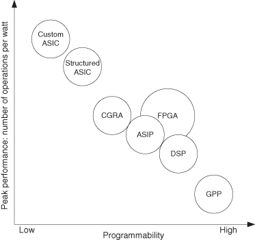
Custom ASIC hardware and software on GPPs can be seen as two extremes in the technology spectrum with different trade-offs in programmability and performance; there are various technologies that lie between these two extremes (Figure 1.6). The two more well-known ones are application-specific instruction processors (ASIPs) and field-programmable gate arrays (FPGAs).
Figure 1.6 A simplified technology comparison: programmability versus performance. GPP, general-purpose processor; CGRA, coarse-grained reconfigurable architecture.
An ASIP is a processor with an instruction set customized for a specific application or domain. Custom instructions efficiently implemented in hardware are often integrated into a base processor with a basic instruction set. This capability often improves upon the conventional approach of using standard instruction sets to fulfill the same task while preserving its flexibility. Chapters 6 and 7 explore further some of the issues involving custom instructions.
An FPGA typically contains an array of computation units, memories, and their interconnections, and all three are usually programmable in the field by application builders. FPGA technology often offers a good compromise: It is faster than software while being more flexible and having shorter development times than custom ASIC hardware implementations; like GPPs, they are offered as off-the-shelf devices that can be programmed without going through chip fabrication. Because of the growing demand for reducing the time to market and the increasing cost of chip fabrication, FPGAs are becoming more popular for implementing digital designs.
Most commercial FPGAs contain an array of fine-grained logic blocks, each only a few bits wide. It is also possible to have the following:
- Coarse-Grained Reconfigurable Architecture (CGRA). It contains logic blocks that process byte-wide or multiple byte-wide data, which can form building blocks of datapaths.
- Structured ASIC. It allows application builders to customize the resources before fabrication. While it offers performance close to that of ASIC, the need for chip fabrication can be an issue.
- Digital Signal Processors (DSPs). The organization and instruction set for these devices are optimized for digital signal processing applications. Like microprocessors, they have a fixed hardware architecture that cannot be reconfigured.
Figure 1.6 compares these technologies in terms of programmability and performance. Chapters 6–8 provide further information about some of these technologies.
1.4 PROCESSOR ARCHITECTURES
Typically, processors are characterized either by their application or by their architecture (or structure), as shown in Tables 1.2 and 1.3. The requirements space of an application is often large, and there is a range of implementation options. Thus, it is usually difficult to associate a particular architecture with a particular application. In addition, some architectures combine different implementation approaches as seen in the PlayStation example of Section 1.1. There, the graphics processor consists of a four-element SIMD array of vector processing functional units (FUs). Other SOC implementations consist of multiprocessors using very long instruction word (VLIW) and/or superscalar processors.
TABLE 1.2 Processor Examples as Identified by Function
| Processor Type | Application |
| Graphics processing unit (GPU) | 3-D graphics; rendering, shading, texture |
| Digital signal processor (DSP) | Generic, sometimes used with wireless |
| Media processor | Video and audio signal processing |
| Network processor | Routing, buffering |
TABLE 1.3 Processor Examples as Identified by Architecture
| Processor Type | Architecture/Implementation Approach |
| SIMD | Single instruction applied to multiple functional units (processors) |
| Vector (VP) | Single instruction applied to multiple pipelined registers |
| VLIW | Multiple instructions issued each cycle under compiler control |
| Superscalar | Multiple instructions issued each cycle under hardware control |
From the programmer’s point of view, sequential processors execute one instruction at a time. However, many processors have the capability to execute several instructions concurrently in a manner that is transparent to the programmer, through techniques such as pipelining, multiple execution units, and multiple cores. Pipelining is a powerful technique that is used in almost all current processor implementations. Techniques to extract and exploit the inherent parallelism in the code at compile time or run time are also widely used.
Exploiting program parallelism is one of the most important goals in computer architecture.
Instruction-level parallelism (ILP) means that multiple operations can be executed in parallel within a program. ILP may be achieved with hardware, compiler, or operating system techniques. At the loop level, consecutive loop iterations are ideal candidates for parallel execution, provided that there is no data dependency between subsequent loop iterations. Next, there is parallelism available at the procedure level, which depends largely on the algorithms used in the program. Finally, multiple independent programs can execute in parallel.
Different computer architectures have been built to exploit this inherent parallelism. In general, a computer architecture consists of one or more interconnected processor elements (PEs) that operate concurrently, solving a single overall problem.
1.4.1 Processor: A Functional View
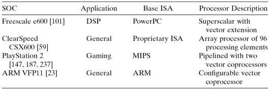
Table 1.4 shows different SOC designs and the processor used in each design. For these examples, we can characterize them as general purpose, or special purpose with support for gaming or signal processing applications. This functional view tells little about the underlying hardware implementation. Indeed, several quite different architectural approaches could implement the same generic function. The graphics function, for example, requires shading, rendering, and texturing functions as well as perhaps a video function. Depending on the relative importance of these functions and the resolution of the created images, we could have radically different architectural implementations.
TABLE 1.4 Processor Models for Different SOC Examples
1.4.2 Processor: An Architectural View
The architectural view of the system describes the actual implementation at least in a broad-brush way. For sophisticated architectural approaches, more detail is required to understand the complete implementation.
Simple Sequential Processor
Sequential processors directly implement the sequential execution model. These processors process instructions sequentially from the instruction stream. The next instruction is not processed until all execution for the current instruction is complete and its results have been committed.
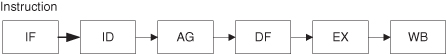
The semantics of the instruction determines that a sequence of actions must be performed to produce the specified result (Figure 1.7). These actions can be overlapped, but the result must appear in the specified serial order. These actions include
1. fetching the instruction into the instruction register (IF),
2. decoding the opcode of the instruction (ID),
3. generating the address in memory of any data item residing there (AG),
4. fetching data operands into executable registers (DF),
5. executing the specified operation (EX), and
6. writing back the result to the register file (WB).
Figure 1.7 Instruction execution sequence.
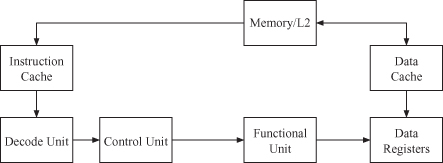
A simple sequential processor model is shown in Figure 1.8. During execution, a sequential processor executes one or more operations per clock cycle from the instruction stream. An instruction is a container that represents the smallest execution packet managed explicitly by the processor. One or more operations are contained within an instruction. The distinction between instructions and operations is crucial to distinguish between processor behaviors. Scalar and superscalar processors consume one or more instructions per cycle, where each instruction contains a single operation.
Figure 1.8 Sequential processor model.
Although conceptually simple, executing each instruction sequentially has significant performance drawbacks: A considerable amount of time is spent on overhead and not on actual execution. Thus, the simplicity of directly implementing the sequential execution model has significant performance costs.
Pipelined Processor
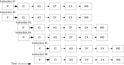
Pipelining is a straightforward approach to exploiting parallelism that is based on concurrently performing different phases (instruction fetch, decode, execution, etc.) of processing an instruction. Pipelining assumes that these phases are independent between different operations and can be overlapped—when this condition does not hold, the processor stalls the downstream phases to enforce the dependency. Thus, multiple operations can be processed simultaneously with each operation at a different phase of its processing. Figure 1.9 illustrates the instruction timing in a pipelined processor, assuming that the instructions are independent.
Figure 1.9 Instruction timing in a pipelined processor.

For a simple pipelined machine, there is only one operation in each phase at any given time; thus, one operation is being fetched (IF); one operation is being decoded (ID); one operation is generating an address (AG); one operation is accessing operands (DF); one operation is in execution (EX); and one operation is storing results (WB). Figure 1.10 illustrates the general form of a pipelined processor. The most rigid form of a pipeline, sometimes called the static pipeline, requires the processor to go through all stages or phases of the pipeline whether required by a particular instruction or not. A dynamic pipeline allows the bypassing of one or more pipeline stages, depending on the requirements of the instruction. The more complex dynamic pipelines allow instructions to complete out of (sequential) order, or even to initiate out of order. The out-of-order processors must ensure that the sequential consistency of the program is preserved. Table 1.5 shows some SOC pipelined “soft” processors.
TABLE 1.5 SOC Examples Using Pipelined Soft Processors [177, 178]. A Soft Processor Is Implemented with FPGAs or Similar Reconfigurable Technology
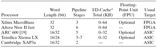
*Means configurable I-cache and/or D-cache.
Figure 1.10 Pipelined processor model.

ILP
While pipelining does not necessarily lead to executing multiple instructions at exactly the same time, there are other techniques that do. These techniques may use some combination of static scheduling and dynamic analysis to perform concurrently the actual evaluation phase of several different operations, potentially yielding an execution rate of greater than one operation every cycle. Since historically most instructions consist of only a single operation, this kind of parallelism has been named ILP (instruction level parallelism).
Two architectures that exploit ILP are superscalar and VLIW processors. They use different techniques to achieve execution rates greater than one operation per cycle. A superscalar processor dynamically examines the instruction stream to determine which operations are independent and can be executed. A VLIW processor relies on the compiler to analyze the available operations (OP) and to schedule independent operations into wide instruction words, which then execute these operations in parallel with no further analysis.
Figure 1.11 shows the instruction timing of a pipelined superscalar or VLIW processor executing two instructions per cycle. In this case, all the instructions are independent so that they can be executed in parallel. The next two sections describe these two architectures in more detail.
Figure 1.11 Instruction timing in a pipelined ILP processor.
Superscalar Processors
Dynamic pipelined processors remain limited to executing a single operation per cycle by virtue of their scalar nature. This limitation can be avoided with the addition of multiple functional units and a dynamic scheduler to process more than one instruction per cycle (Figure 1.12). These superscalar processors [135] can achieve execution rates of several instructions per cycle (usually limited to two, but more is possible depending on the application). The most significant advantage of a superscalar processor is that processing multiple instructions per cycle is done transparently to the user, and that it can provide binary code compatibility while achieving better performance.
Figure 1.12 Superscalar processor model.

Compared to a dynamic pipelined processor, a superscalar processor adds a scheduling instruction window that analyzes multiple instructions from the instruction stream in each cycle. Although processed in parallel, these instructions are treated in the same manner as in a pipelined processor. Before an instruction is issued for execution, dependencies between the instruction and its prior instructions must be checked by hardware.
Because of the complexity of the dynamic scheduling logic, high-performance superscalar processors are limited to processing four to six instructions per cycle. Although superscalar processors can exploit ILP from the dynamic instruction stream, exploiting higher degrees of parallelism requires other approaches.
VLIW Processors
In contrast to dynamic analyses in hardware to determine which operations can be executed in parallel, VLIW processors (Figure 1.13) rely on static analyses in the compiler.
Figure 1.13 VLIW processor model.
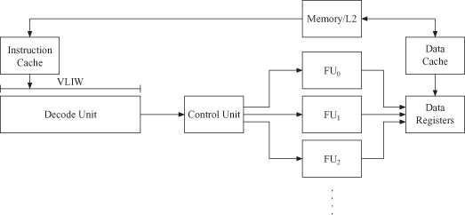
VLIW processors are thus less complex than superscalar processors and have the potential for higher performance. A VLIW processor executes operations from statically scheduled instructions that contain multiple independent operations. Because the control complexity of a VLIW processor is not significantly greater than that of a scalar processor, the improved performance comes without the complexity penalties.
VLIW processors rely on the static analyses performed by the compiler and are unable to take advantage of any dynamic execution characteristics. For applications that can be scheduled statically to use the processor resources effectively, a simple VLIW implementation results in high performance. Unfortunately, not all applications can be effectively scheduled statically. In many applications, execution does not proceed exactly along the path defined by the code scheduler in the compiler. Two classes of execution variations can arise and affect the scheduled execution behavior:
1. delayed results from operations whose latency differs from the assumed latency scheduled by the compiler and
2. interruptions from exceptions or interrupts, which change the execution path to a completely different and unanticipated code schedule.
Although stalling the processor can control a delayed result, this solution can result in significant performance penalties. The most common execution delay is a data cache miss. Many VLIW processors avoid all situations that can result in a delay by avoiding data caches and by assuming worst-case latencies for operations. However, when there is insufficient parallelism to hide the exposed worst-case operation latency, the instruction schedule has many incompletely filled or empty instructions, resulting in poor performance.
Tables 1.6 and 1.7 describe some representative superscalar and VLIW processors.
TABLE 1.6 SOC Examples Using Superscalar Processors
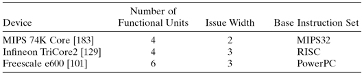
TABLE 1.7 SOC Examples Using VLIW Processors
| Device | Number of Functional Units | Issue Width |
| Fujitsu MB93555A [103] | 8 | 8 |
| TI TMS320C6713B [243] | 8 | 8 |
| CEVA-X1620 [54] | 30 | 8 |
| Philips Nexperia PNX1700 [199] | 30 | 5 |
SIMD Architectures: Array and Vector Processors
The SIMD class of processor architecture includes both array and vector processors. The SIMD processor is a natural response to the use of certain regular data structures, such as vectors and matrices. From the view of an assembly-level programmer, programming SIMD architecture appears to be very similar to programming a simple processor except that some operations perform computations on aggregate data. Since these regular structures are widely used in scientific programming, the SIMD processor has been very successful in these environments.
The two popular types of SIMD processor are the array processor and the vector processor. They differ both in their implementations and in their data organizations. An array processor consists of many interconnected processor elements, each having their own local memory space. A vector processor consists of a single processor that references a global memory space and has special function units that operate on vectors.
An array processor or a vector processor can be obtained by extending the instruction set to an otherwise conventional machine. The extended instructions enable control over special resources in the processor, or in some sort of coprocessor. The purpose of such extensions is to enable increased performance on special applications.
Array Processors
The array processor (Figure 1.14) is a set of parallel processor elements connected via one or more networks, possibly including local and global interelement communications and control communications. Processor elements operate in lockstep in response to a single broadcast instruction from a control processor (SIMD). Each processor element (PE) has its own private memory, and data are distributed across the elements in a regular fashion that is dependent on both the actual structure of the data and also the computations to be performed on the data. Direct access to global memory or another processor element’s local memory is expensive, so intermediate values are propagated through the array through local interprocessor connections. This requires that the data be distributed carefully so that the routing required to propagate these values is simple and regular. It is sometimes easier to duplicate data values and computations than it is to support a complex or irregular routing of data between processor elements.
Figure 1.14 Array processor model.

Since instructions are broadcast, there is no means local to a processor element of altering the flow of the instruction stream; however, individual processor elements can conditionally disable instructions based on local status information—these processor elements are idle when this condition occurs. The actual instruction stream consists of more than a fixed stream of operations. An array processor is typically coupled to a general-purpose control processor that provides both scalar operations as well as array operations that are broadcast to all processor elements in the array. The control processor performs the scalar sections of the application, interfaces with the outside world, and controls the flow of execution; the array processor performs the array sections of the application as directed by the control processor.
A suitable application for use on an array processor has several key characteristics: a significant amount of data that have a regular structure, computations on the data that are uniformly applied to many or all elements of the data set, and simple and regular patterns relating the computations and the data. An example of an application that has these characteristics is the solution of the Navier–Stokes equations, although any application that has significant matrix computations is likely to benefit from the concurrent capabilities of an array processor.
Table 1.8 contains several array processor examples. The ClearSpeed processor is an example of an array processor chip that is directed at signal processing applications.
TABLE 1.8 SOC Examples Based on Array Processors
| Device | Processors per Control Unit | Data Size (bit) |
| ClearSpeed CSX600 [59] | 96 | 32 |
| Atsana J2211 [174] | Configurable | 16/32 |
| Xelerator X10q [257] | 200 | 4 |
Vector Processors
A vector processor is a single processor that resembles a traditional single stream processor, except that some of the function units (and registers) operate on vectors—sequences of data values that are seemingly operated on as a single entity. These function units are deeply pipelined and have high clock rates. While the vector pipelines often have higher latencies compared with scalar function units, the rapid delivery of the input vector data elements, together with the high clock rates, results in a significant throughput.
Modern vector processors require that vectors be explicitly loaded into special vector registers and stored back into memory—the same course that modern scalar processors use for similar reasons. Vector processors have several features that enable them to achieve high performance. One feature is the ability to concurrently load and store values between the vector register file and the main memory while performing computations on values in the vector register file. This is an important feature since the limited length of vector registers requires that vectors longer than the register length would be processed in segments—a technique called strip mining. Not being able to overlap memory accesses and computations would pose a significant performance bottleneck.
Most vector processors support a form of result bypassing—in this case called chaining—that allows a follow-on computation to commence as soon as the first value is available from the preceding computation. Thus, instead of waiting for the entire vector to be processed, the follow-on computation can be significantly overlapped with the preceding computation that it is dependent on. Sequential computations can be efficiently compounded to behave as if they were a single operation, with a total latency equal to the latency of the first operation with the pipeline and chaining latencies of the remaining operations, but none of the start-up overhead that would be incurred without chaining. For example, division could be synthesized by chaining a reciprocal with a multiply operation. Chaining typically works for the results of load operations as well as normal computations.
A typical vector processor configuration (Figure 1.15) consists of a vector register file, one vector addition unit, one vector multiplication unit, and one vector reciprocal unit (used in conjunction with the vector multiplication unit to perform division); the vector register file contains multiple vector registers (elements).
Figure 1.15 Vector processor model.

Table 1.9 shows examples of vector processors. The IBM mainframes have vector instructions (and support hardware) as an option for scientific users.
TABLE 1.9 SOC Examples Using Vector Processor
| Device | Vector Function Units | Vector Registers |
| Freescale e600 [101] | 4 | 32 Configurable |
| Motorola RSVP [58] | 4 (64 bit partitionable at 16 bits) | 2 streams (each 2 from, 1 to) memory |
| ARM VFP11 [23] | 3 (64 bit partitionable to 32 bits) | 4 × 8, 32 bit |
Configurable implies a pool of N registers that can be configured as p register sets of N/p elements.
Multiprocessors
Multiple processors can cooperatively execute to solve a single problem by using some form of interconnection for sharing results. In this configuration, each processor executes completely independently, although most applications require some form of synchronization during execution to pass information and data between processors. Since the multiple processors share memory and execute separate program tasks (MIMD [multiple instruction stream, multiple data stream]), their proper implementation is significantly more complex then the array processor. Most configurations are homogeneous with all processor elements being identical, although this is not a requirement. Table 1.10 shows examples of SOC multiprocessors.
TABLE 1.10 SOC Multiprocessors and Multithreaded Processors

The interconnection network in the multiprocessor passes data between processor elements and synchronizes the independent execution streams between processor elements. When the memory of the processor is distributed across all processors and only the local processor element has access to it, all data sharing is performed explicitly using messages, and all synchronization is handled within the message system. When the memory of the processor is shared across all processor elements, synchronization is more of a problem—certainly, messages can be used through the memory system to pass data and information between processor elements, but this is not necessarily the most effective use of the system.
When communications between processor elements are performed through a shared memory address space—either global or distributed between processor elements (called distributed shared memory to distinguish it from distributed memory)—there are two significant problems that arise. The first is maintaining memory consistency: the programmer-visible ordering effects on memory references, both within a processor element and between different processor elements. This problem is usually solved through a combination of hardware and software techniques. The second is cache coherency—the programmer-invisible mechanism to ensure that all processor elements see the same value for a given memory location. This problem is usually solved exclusively through hardware techniques.
The primary characteristic of a multiprocessor system is the nature of the memory address space. If each processor element has its own address space (distributed memory), the only means of communication between processor elements is through message passing. If the address space is shared (shared memory), communication is through the memory system.
The implementation of a distributed memory machine is far easier than the implementation of a shared memory machine when memory consistency and cache coherency are taken into account. However, programming a distributed memory processor can be much more difficult since the applications must be written to exploit and not to be limited by the use of message passing as the only form of communication between processor elements. On the other hand, despite the problems associated with maintaining consistency and coherency, programming a shared memory processor can take advantage of whatever communications paradigm is appropriate for a given communications requirement, and can be much easier to program.
1.5 MEMORY AND ADDRESSING
SOC applications vary significantly in memory requirements. In one case, the memory structure can be as simple as the program residing entirely in an on-chip read-only memory (ROM), with the data in on-chip RAM. In another case, the memory system might support an elaborate operating system requiring a large off-chip memory (system on a board), with a memory management unit and cache hierarchy.
Why not simply include memory with the processor on the die? This has many attractions:
1. It improves the accessibility of memory, improving both memory access time and bandwidth.
2. It reduces the need for large cache.
3. It improves performance for memory-intensive applications.
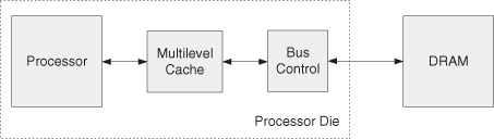
But there are problems. The first problem is that DRAM memory process technology differs from standard microprocessor process technology, and would cause some sacrifice in achievable bit density. The second problem is more serious: If memory were restricted to the processor die, its size would be correspondingly limited. Applications that require very large real memory space would be crippled. Thus, the conventional processor die model has evolved (Figure 1.16) to implement multiple robust homogeneous processors sharing the higher levels of a two- or three-level cache structure with the main memory off-die, on its own multidie module.
Figure 1.16 Processors with memory off-die.
From a design complexity point of view, this has the advantage of being a “universal” solution: One implementation fits all applications, although not necessarily equally well. So, while a great deal of design effort is required for such an implementation, the production quantities can be large enough to justify the costs.
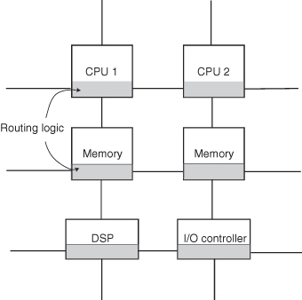
An alternative to this approach is clear. For specific applications, whose memory size can be bounded, we can implement an integrated memory SOC. This concept is illustrated in Figure 1.17 (also recall Figure 1.3).
Figure 1.17 System on a chip: processors and memory.

A related but separate question is: Does the application require virtual memory (mapping disk space onto memory) or is all real memory suitable? We look at the requirement for virtual memory addressing in the next section.
Finally, the memory can be centralized or distributed. Even here, the memory can appear to the programmer as a single (centralized) shared memory, even though it is implemented in several distributed modules. Several memory considerations are listed in Table 1.11.
TABLE 1.11 SOC Memory Considerations
| Issue | Implementation | Comment |
| Memory placement | On-die | Limited and fixed size |
| Off-die | System on a board, slow access, limited bandwidth | |
| Addressing | Real addressing | Limited size, simple OS |
| Virtual addressing | Much more complex, require TLB, in-order instruction execution support | |
| Arrangement (as programmed for multiple processors) | Shared memory | Requires hardware support |
| Message passing | Additional programming | |
| Arrangement (as implemented) | Centralized | Limited by chip considerations |
| Distributed | Can be clustered with a processor or other memory modules |
The memory system comprises the physical storage elements in the memory hierarchy. These elements include those specified by the instruction set (registers, main memory, and disk sectors) as well as those elements that are largely transparent to the user’s program (buffer registers, cache, and page mapped virtual memory).
1.5.1 SOC Memory Examples
Table 1.12 shows a number of different SOC designs and their cache and memory configuration. It is important for SOC designers to consider whether to put RAM and ROM on-die or off-die. Table 1.13 shows various examples of SOC embedded memory macro cell.
TABLE 1.12 Memory Hierarchy for Different SOC Examples
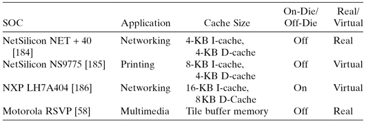
TABLE 1.13 Example SOC Embedded Memory Macro Cell (See Chapter 4 for the Discussion on Cell Types)
| Vendor | Cell Type (Typical) | SOC User (Typical) |
| Virage Logic | 6T (SRAM) | SigmaTel/ARM |
| ATMOS | 1T (eDRAM) | Philips |
| IBM | 1T (eDRAM) | IBM |
Note: T refers to the number of transistors in a 1-bit cell.
1.5.2 Addressing: The Architecture of Memory
The user’s view of memory primarily consists of the addressing facilities available to the programmer. Some of these facilities are available to the application programmer and some to the operating system programmer. Virtual memory enables programs requiring larger storage than the physical memory to run and allows separation of address spaces to protect unauthorized access to memory regions when executing multiple application programs. When virtual addressing facilities are properly implemented and programmed, memory can be efficiently and securely accessed.
Virtual memory is often supported by a memory management unit. Conceptually, the physical memory address is determined by a sequence of (at least) three steps:
1. The application produces a process address. This, together with the process or user ID, defines the virtual address: virtual address = offset + (program) base + index, where the offset is specified in the instruction while the base and index values are in specified registers.
2. Since multiple processes must cooperate in the same memory space, the process addresses must be coordinated and relocated. This is typically done by a segment table. Upper bits of the virtual address are used to address a segment table, which has a (predetermined) base and bound values for the process, resulting in a system address: system address = virtual address + (process) base, where the system address must be less than the bound.
3. Virtual versus real. For many SOC applications (and all generic systems), the memory space exceeds the available (real) implemented memory. Here the memory space is implemented on disk and only the recently used regions (pages) are brought into memory. The available pages are located by a page table. The upper bits of the system address access a page table. If the data for this page have been loaded from the disk, the location in memory will be provided as the upper address bits of the “real” or physical memory address. The lower bits of the real address are the same as the corresponding lower bits of the virtual address.
Usually, the tables (segment and page) performing address translation are in memory, and a mechanism for the translation called the translation lookaside buffer (TLB) must be used to speed up this translation. A TLB is a simple register system, usually consisting of between 64 and 256 entries, that saves recent address translations for reuse. A small number of (hashed) virtual address bits address the TLB. The TLB entry has both the real address and the complete virtual address (and ID). If the virtual address matches, the real address from the TLB can be used. Otherwise, a not-in-TLB event occurs and a complete translation must occur (Figure 1.18).
Figure 1.18 Virtual-to-real address mapping with a TLB bypass.

1.5.3 Memory for SOC Operating System
One of the most critical decisions (or requirements) concerning an SOC design is the selection of the operating system and its memory management functionality. Of primary interest to the designer is the requirement for virtual memory. If the system can be restricted to a real memory (physically, not virtually addressed) and the size of the memory can be contained to the order of 10 s of megabytes, the system can be implemented as a true system on a chip (all memory on-die). The alternative, virtual memory, is often slower and significantly more expensive, requiring a complex memory management unit. Table 1.14 illustrates some current SOC designs and their operating systems.
TABLE 1.14 Operating Systems for SOC Designs
| OS | Vendor | Memory Model |
| uClinux | Open source | Real |
| VxWorks (RTOS) [254] | Wind River | Real |
| Windows CE | Microsoft | Virtual |
| Nucleus (RTOS) [175] | Mentor Graphics | Real |
| MQX (RTOS) [83] | ARC | Real |
Of course, fast real memory designs come at the price of functionality. The user has limited ways of creating new processes and of expanding the application base of the systems.
1.6 SYSTEM-LEVEL INTERCONNECTION
SOC technology typically relies on the interconnection of predesigned circuit modules (known as intellectual property [IP] blocks) to form a complete system, which can be integrated onto a single chip. In this way, the design task is raised from a circuit level to a system level. Central to the system-level performance and the reliability of the finished product is the method of interconnection used. A well-designed interconnection scheme should have vigorous and efficient communication protocols, unambiguously defined as a published standard. This facilitates interoperability between IP blocks designed by different people from different organizations and encourages design reuse. It should provide efficient communication between different modules maximizing the degree of parallelism achieved.
SOC interconnect methods can be classified into two main approaches: buses and network-on-chip, as illustrated in Figures 1.19 and 1.20.
Figure 1.19 SOC system-level interconnection: bus-based approach.
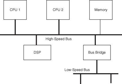
Figure 1.20 SOC system-level interconnection: network-on-chip approach.
1.6.1 Bus-Based Approach
With the bus-based approach, IP blocks are designed to conform to published bus standards (such as ARM’s Advanced Microcontroller Bus Architecture [AMBA] [21] or IBM’s CoreConnect [124]). Communication between modules is achieved through the sharing of the physical connections of address, data, and control bus signals. This is a common method used for SOC system-level interconnect. Usually, two or more buses are employed in a system, organized in a hierarchical fashion. To optimize system-level performance and cost, the bus closest to the CPU has the highest bandwidth, and the bus farthest from the CPU has the lowest bandwidth.
1.6.2 Network-on-Chip Approach
A network-on-chip system consists of an array of switches, either dynamically switched as in a crossbar or statically switched as in a mesh.
The crossbar approach uses asynchronous channels to connect synchronous modules that can operate at different clock frequencies. This approach has the advantage of higher throughput than a bus-based system while making integration of a system with multiple clock domains easier.
In a simple statically switched network (Figure 1.20), each node contains processing logic forming the core, and its own routing logic. The interconnect scheme is based on a two-dimensional mesh topology. All communications between switches are conducted through data packets, routed through the router interface circuit within each node. Since the interconnections between switches have a fixed distance, interconnect-related problems such as wire delay and cross talk noise are much reduced. Table 1.15 lists some interconnect examples used in SOC designs.
TABLE 1.15 Interconnect Models for Different SOC Examples
| SOC | Application | Interconnect Type |
| ClearSpeed CSX600 [59] | High Performance Computing | ClearConnect bus |
| NetSilicon NET +40 [184] | Networking | Custom bus |
| NXP LH7A404 [186] | Networking | AMBA bus |
| Intel PXA27x [132] | Mobile/wireless | PXBus |
| Matsushita i-Platform [176] | Media | Internal connect bus |
| Emulex InSpeed SOC320 [130] | Switching | Crossbar switch |
| MultiNOC [172] | Multiprocessing system | Network-on-chip |
1.7 AN APPROACH FOR SOC DESIGN
Two important ideas in a design process are figuring out the requirements and specifications, and iterating through different stages of design toward an efficient and effective completion.
1.7.1 Requirements and Specifications
Requirements and specifications are fundamental concepts in any system design situation. There must be a thorough understanding of both before a design can begin. They are useful at the beginning and at the end of the design process: at the beginning, to clarify what needs to be achieved; and at the end, as a reference against which the completed design can be evaluated.
The system requirements are the largely externally generated criteria for the system. They may come from competition, from sales insights, from customer requests, from product profitability analysis, or from a combination. Requirements are rarely succinct or definitive of anything about the system. Indeed, requirements can frequently be unrealistic: “I want it fast, I want it cheap, and I want it now!”
It is important for the designer to analyze carefully the requirements expressions, and to spend sufficient time in understanding the market situation to determine all the factors expressed in the requirements and the priorities those factors imply. Some of the factors the designer considers in determining requirements include
- compatibility with previous designs or published standards,
- reuse of previous designs,
- customer requests/complaints,
- sales reports,
- cost analysis,
- competitive equipment analysis, and
- trouble reports (reliability) of previous products and competitive products.
The designer can also introduce new requirements based on new technology, new ideas, or new materials that have not been used in a similar systems environment.
The system specifications are the quantified and prioritized criteria for the target system design. The designer takes the requirements and must produce a succinct and definitive set of statements about the eventual system. The designer may have no idea of what the eventual system will look like, but usually, there is some “straw man” design in mind that seems to provide a feasibility framework to the specification. In any effective design process, it would be surprising if the final design significantly resembles the straw man design.
The specification does not complete any part of the design process; it initializes the process. Now the design can begin with the selection of components and approaches, the study of alternatives, and the optimization of the parts of the system.
1.7.2 Design Iteration
Design is always an iterative process. So, the obvious question is how to get the very first, initial design. This is the design that we can then iterate through and optimize according to the design criteria. For our purposes, we define several types of designs based on the stage of design effort.
Initial Design
This is the first design that shows promise in meeting the key requirements, while other performance and cost criteria are not considered. For instance, processor or memory or input/output (I/O) should be sized to meet high-priority real-time constraints. Promising components and their parameters are selected and analyzed to provide an understanding of their expected idealized performance and cost. Idealized does not mean ideal; it means a simplified model of the expected area occupied and computational or data bandwidth capability. It is usually a simple linear model of performance, such as the expected million instructions per second (MIPS) rate of a processor.
Optimized Design
Once the base performance (or area) requirements are met and the base functionality is ensured, then the goal is to minimize the cost (area) and/or the power consumption or the design effort required to complete the design. This is the iterative step of the process. The first steps of this process use higher-fidelity tools (simulations, trial layouts, etc.) to ensure that the initial design actually does satisfy the design specifications and requirements. The later steps refine, complete, and improve the design according to the design criteria.
Figure 1.21 shows the steps in creating an initial design. This design is detailed enough to create a component view of the design and a corresponding projection of the component’s expected performance. This projection is, at this step, necessarily simplified and referenced to here as the idealized view of the component (Figure 1.22).
Figure 1.21 The SOC initial design process.

Figure 1.22 Idealized SOC components.

System performance is limited by the component with the least capability. The other components can usually be modeled as simply presenting a delay to the critical component. In a good design, the most expensive component is the one that limits the performance of the system. The system’s ability to process transactions should closely follow that of the limiting component. Typically, this is the processor or memory complex.
Usually, designs are driven by either (1) a specific real-time requirement, after which functionality and cost become important, or (2) functionality and/or throughput under cost–performance constraints. In case (1), the real-time constraint is provided by I/O consideration, which the processor–memory–interconnect system must meet. The I/O system then determines the performance, and any excess capability of the remainder of the system is usually used to add functionality to the system. In case (2), the object is to improve task throughput while minimizing the cost. Throughput is limited by the most constrained component, so the designer must fully understand the trade-offs at that point. There is more flexibility in these designs, and correspondingly more options in determining the final design.
The purpose of this book is to provide an approach for determining the initial design by
(a) describing the range of components—processors, memories, and interconnects—that are available in building an SOC;
(b) providing examples of requirements for various domains of applications, such as data compression and encryption; and
(c) illustrating how an initial design, or a reported implementation, can show promise in meeting specific requirements.
We explain this approach in Chapters 3–5 on a component by component basis to cover (a), with Chapter 6 covering techniques for system configuration and customization. Chapter 7 contains application studies to cover (b) and (c).
As mentioned earlier, the designer must optimize each component for processing and storage. This optimization process requires extensive simulation. We provide access to basic simulation tools through our associated web site.
1.8 SYSTEM ARCHITECTURE AND COMPLEXITY
The basic difference between processor architecture and system architecture is that the system adds another layer of complexity, and the complexity of these systems limits the cost savings. Historically, the notion of a computer is a single processor plus a memory. As long as this notion is fixed (within broad tolerances), implementing that processor on one or more silicon die does not change the design complexity. Once die densities enable a scalar processor to fit on a chip, the complexity issue changes.
Suppose it takes about 100,000 transistors to implement a 32-bit pipelined processor with a small first-level cache. Let this be a processor unit of design complexity.
As long as we need to implement the 100,000 transistor processors, additional transistor density on the die does not much affect design complexity. More transistors per die, while increasing die complexity, simplify the problem of interconnecting multiple chips that make up the processor. Once the unit processor is implemented on a single die, the design complexity issue changes. As transistor densities significantly improve after this point, there are obvious processor extension strategies to improve performance:
1. Additional Cache. Here we add cache storage and, as large caches have slower access times, a second-level cache.
2. A More Advanced Processor. We implement a superscalar or a VLIW processor that executes more than one instruction each cycle. Additionally, we speed up the execution units that affect the critical path delay, especially the floating-point execution times.
3. Multiple Processors. Now we implement multiple (superscalar) processors and their associated multilevel caches. This leaves us limited only by the memory access times and bandwidth.
The result of the above is a significantly greater design complexity (see Figure 1.23). Instead of the 100,000 transistor processors, our advanced processor has millions of transistors; the multilevel caches are also complex, as is the need to coordinate (synchronize) the multiple processors, since they require a consistent image of the contents of memory.
Figure 1.23 Complexity of design.

The obvious way to manage this complexity is to reuse designs. So, reusing several simpler processor designs implemented on a die is preferable to a new, more advanced, single processor. This is especially true if we can select specific processor designs suited to particular parts of an application. For this to work, we also need a robust interconnection mechanism to access the various processors and memory.
So, when an application is well specified, the system-on-a-chip approach includes
1. multiple (usually) heterogeneous processors, each specialized for specific parts of the application;
2. the main memory with (often) ROM for partial program storage;
3. a relatively simple, small (single-level) cache structure or buffering schemes associated with each processor; and
4. a bus or switching mechanism for communications.
Even when the SOC approach is technically attractive, it has economic limitations and implications. Given the processor and interconnect complexity, if we limit the usefulness of an implementation to a particular application, we have to either (1) ensure that there is a large market for the product or (2) find methods for reducing the design cost through design reuse or similar techniques.
1.9 PRODUCT ECONOMICS AND IMPLICATIONS FOR SOC
1.9.1 Factors Affecting Product Costs
The basic cost and profitability of a product depend on many factors: its technical appeal, its cost, the market size, and the effect the product has on future products. The issue of cost goes well beyond the product’s manufacturing cost.
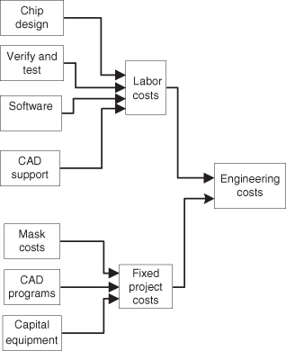
There are fixed and variable costs, as shown in Figure 1.24. Indeed, the engineering costs, frequently the largest of the fixed costs, are expended before any revenue can be realized from sales (Figure 1.25).
Figure 1.24 Project cost components.

Figure 1.25 Engineering (development) costs.
Depending on the complexity, designing a new chip requires a development effort of anywhere between 12 and 30 months before the first manufactured unit can be shipped. Even a moderately sized project may require up to 30 or more hardware and software engineers, CAD design, and support personnel. For instance, the paper describing the Sony Emotion Engine has 22 authors [147, 187]. However, their salary and indirect costs might represent only a fraction of the total development cost.
Nonengineering fixed costs include manufacturing start-up costs, inventory costs, initial marketing and sales costs, and administrative overhead. The marketing costs include obvious items such as market research, strategic market planning, pricing studies, and competitive analysis, and so on, as well as sales planning and advertising costs. The concept of general and administrative (G & A) “overhead” includes a proportional share of the “front office”—the executive management, personnel department (human resources), financial office, and other costs.
Later, in the beginning of the manufacturing process, unit cost remains high. It is not until many units are shipped that the marginal manufacturing cost can approach the ultimate manufacturing costs.
After this, manufacturing produces units at a cost increasingly approaching the ultimate manufacturing cost. Still, during this time, there is a continuing development effort focused on extending the life of the product and broadening its market applicability.
Will the product make a profit? From the preceding discussion, it is easy to see how sensitive the cost is to the product life and to the number of products shipped. If market forces or the competition is aggressive and produces rival systems with expanded performance, the product life may be shortened and fewer units may be delivered than expected. This could be disastrous even if the ultimate manufacturing cost is reached; there may not be enough units to amortize the fixed costs and ensure profit. On the other hand, if competition is not aggressive and the follow-on development team is successful in enhancing the product and continuing its appeal in the marketplace, the product can become one of those jewels in a company’s repertoire, bringing fame to the designers and smiles to the stockholders.
1.9.2 Modeling Product Economics and Technology Complexity: The Lesson for SOC
To put all this into perspective, consider a general model of a product’s average unit cost (as distinct from its ultimate manufactured cost):
![]()
The product cost is simply the sum of all the fixed and variable costs. We represent the fixed cost as a constant, Kf. It is also clear that the variable costs are of the form Kv × n, where n is the number of units. However, there are certain ongoing engineering, sales, and marketing costs that are related to n but are not necessarily linear.
Let us assume that we can represent this effect as a term that starts as 0.1 of Kf and then slowly increases with n, say, ![]() . So, we get
. So, we get
We can use Equation 1.1 to illustrate the effects of advancing technology on product design. We compare a design done in 1995 with a more complex 2005 design, which has a much lower production cost. With Kf fixed, Figure 1.26 shows the expected decrease in unit cost as the volume of 1995 products produced, n, increases. But the figure also shows that, if we increase the fixed costs (more complex designs) by 10-fold, even if we cut the unit costs (Kv) by the same amount, the 2005 unit product costs remain high until much larger volumes are reached. This might not be a problem for a “universal” processor design with a mass market, but it can be a challenge for those SOC designs targeted at specific applications, which may have limited production volume; a more specific design will be more efficient for a particular application, at the expense of generality, which affects volume.
Figure 1.26 The effect of volume on unit cost.

1.10 DEALING WITH DESIGN COMPLEXITY
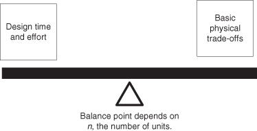
As design cost and complexity increase, there is a basic trade-off between the design optimization of the physical product and the cost of the design. This is shown in Figure 1.27. The balance point depends on n, the number of units expected to be produced. There are several approaches to the design productivity problem. The most basic approaches are purchasing predesigned components and utilizing reconfigurable devices.
Figure 1.27 The design effort must balance volume.
1.10.1 Buying IP
If the goal is to produce a design optimized in the use of the technology, the fixed costs will be high, so the result must be broadly applicable. The alternative to this is to “reuse” the existing design. These may be suboptimal for all the nuances of a particular process technology, but the savings in design time and effort can be significant. The purchase of such designs from third parties is referred to as the sale of IP.
The use of IP reduces the risk in design development: It is intended to reduce the design costs and improves the time to market. The cost of an IP usually depends on the volume. Hence, the adoption of an IP approach tends to reduce Kf at the expense of increasing Kv in Equation 1.1.
Specialized SOC designs often use several different types of processors. Noncritical and specialized processors are purchased as IP and are integrated into the design. For example, the ARM7TDMA is a popular licensed 32-bit processor or “core” design. Generally, processor cores can be designed and licensed in a number of ways as shown in Table 1.16.
TABLE 1.16 Types of Processor Cores Available as IP
| Type of Design | Design Level | Description |
| Customized hard IP | Physical level | IP used in fixed process, optimized |
| Synthesized firm IP | Gate level | IP used in multiple processes but some optimization possible |
| Synthesizable soft IP | Register transfer level (RTL) | IP used in any process, nonoptimized |
Hard IPs are physical-level designs that use all features available in a process technology, including circuit design and physical layout. Many analog IPs and mixed-signal IPs (such as SRAM, phase-locked loop) are distributed in this format to ensure optimal timing and other design characteristics. Firm IPs are gate-level designs that include device sizing but are applicable to many fab facilities with different processor technologies. Soft IPs are logic-level designs in synthesizable format and are directly applicable to standard cell technologies. This approach allows users to adapt the source code to fit their design over a broad range of situations.
Clearly, the more optimized designs from the manufacturer are usually less customizable by the user, but they often have better physical, cost–performance trade-offs. There are potential performance–cost–power overheads in delaying the customization process, since the design procedure and even the product technology itself would have to support user customization. Moreover, customizing a design may also necessitate reverification to ensure its correctness. Current technologies, such as the reconfiguration technology described below, aim to maximize the advantages of late customization, such as risk reduction and improvement of time to market. At the same time, they aim to minimize the associated disadvantages, for instance, by introducing hardwired, nonprogrammable blocks to support common operations such as integer multiplication; such hardwired blocks are more efficient than reconfigurable resources, but they are not as flexible.
1.10.2 Reconfiguration
The term reconfiguration refers to a number of approaches that enable the same circuitry to be reused in many applications. A reconfigurable device can also be thought of as a type of purchased IP in which the cost and risk of fabrication are eliminated, while the support for user customization would raise the unit cost. In other words, the adoption of reconfigurable devices would tend to reduce Kf at the expense of increasing Kv in Equation 1.1.
The best-known example of this approach is FPGA technology. An FPGA consists of a large array of cells. Each cell consists of a small lookup table, a flip-flop, and perhaps an output selector. The cells are interconnected by programmable connections, enabling flexible routing across the array (Figure 1.28). Any logic function can be implemented on the FPGA by configuring the lookup tables and the interconnections. Since an array can consist of over 100,000 cells, it can easily define a processor. An obvious disadvantage of the FPGA-based soft processor implementation is its performance–cost–power. The approach has many advantages, however:
1. Circuit fabrication costs increase exponentially with time; hence, it would not be economical to fabricate a circuit unless it can support a large volume. FPGAs themselves are general-purpose devices and are expected to be produced in large volume.
2. The design time for FPGA implementations is low compared to designing a chip for fabrication. There are extensive libraries of designs available for use. This is particularly important for designs for which a short time to market is critical.
3. FPGAs can be used for rapid prototyping of circuits that would be fabricated. In this approach, one or more FPGAs are configured according to the proposed design to emulate it, as a form of “in-circuit emulation.” Programs are run and design errors can be detected.
4. The reconfigurability of FPGAs enables in-system upgrade, which helps to increase the time in market of a product; this capability is especially valuable for applications where new functions or new standards tend to emerge rapidly.
5. The FPGA can be configured to suit a portion of a task and then reconfigured for the remainder of the task (called “run-time reconfiguration”). This enables specialized functional units for certain computations to adapt to environmental changes.
6. In a number of compute-intensive applications, FPGAs can be configured as a very efficient systolic computational array. Since each FPGA cell has one or more storage elements, computations can be pipelined with very fine granularity. This can provide an enormous computational bandwidth, resulting in impressive speedup on selected applications. Some devices, such as the Stretch S5 software configurable processor, couple a conventional processor with an FPGA array [25].
Figure 1.28 The FPGA array.

Reconfiguration and FPGAs play an important part in efficient SOC design. We shall explore them in more detail in the next chapter.
1.11 CONCLUSIONS
Building modern processors or targeted application systems is a complex undertaking. The great advantages offered by the technology—hundreds of millions of transistors on a die—comes at a price, not the silicon itself, but the enormous design effort that is required to implement and support the product.
There are many aspects of SOC design, such as high-level descriptions, compilation technologies, and design flow, that are not mentioned in this chapter. Some of these will be covered later.
In the following chapters, we shall first take a closer look at basic trade-offs in the technology: time, area, power, and reconfigurability. Then, we shall look at some of the details that make up the system components: the processor, the cache, and the memory, and the bus or switch interconnecting them. Next, we cover design and implementation issues from the perspective of customization and configurability. This is followed by a discussion of SOC design flow and application studies. Finally, some challenges facing future SOC technology are presented.
The goal of the text is to help system designers identify the most efficient design choices, together with the mechanisms to manage the design complexity by exploiting the advances in technology.
1.12 PROBLEM SET
1. Suppose the TLB in Figure 1.18 had 256 entries (directly addressed). If the virtual address is 32 bits, the real memory is 512 MB and the page size is 4 KB, show the possible layout of a TLB entry. What is the purpose of the user ID in Figure 1.18 and what is the consequence of ignoring it?
2. Discuss possible arrangement of addressing the TLB.
3. Find an actual VLIW instruction format. Describe the layout and the constraints on the program in using the applications in a single instruction.
4. Find an actual vector instruction for vector ADD. Describe the instruction layout. Repeat for vector load and vector store. Is overlapping of vector instruction execution permitted? Explain.
5. For the pipelined processor in Figure 1.9, suppose instruction #3 sets the CC (condition code that can be tested by following a branch instruction) at the end of WB and instruction #4 is the condition branch. Without additional hardware support, what is the delay in executing instruction #5 if the branch is taken and if the branch is not taken?
6. Suppose we have four different processors; each does 25% of the application. If we improve two of the processors by 10 times, what would be the overall application speedup?
7. Suppose we have four different processors and all but one are totally limited by the bus. If we speed up the bus by three times and assume the processor performance also scales, what is the application speedup?
8. For the pipelined processor in Figure 1.9, assume the cache miss rate is 0.05 per instruction execution and the total cache miss delay is 20 cycles. For this processor, what is the achievable cycle per instruction (CPI)? Ignore other delays, such as branch delays.
9. Design validation is a very important SOC design consideration. Find several approaches specific to SOC designs. Evaluate each from the perspective of a small SOC vendor.
10. Find (from the Internet) two new VLIW DSPs. Determine the maximum number of operations issued in each cycle and the makeup of the operations (number of integer, floating point, branch, etc.). What is the stated maximum performance (operations per second)? Find out how this number was computed.
11. Find (from the Internet) two new, large FPGA parts. Determine the number of logic blocks (configurable logic blocks [CLBs]), the minimum cycle time, and the maximum allowable power consumption. What soft processors are supported?