
Chapter 3
Reconfigurable Antennas
3.1 Introduction
To support a variety of applications, such as communication, navigation, and surveillance, most wireless systems require more than one antenna. These antennas, which may work at different frequencies and polarizations, are usually installed at a number of positions on a wireless platform, such as a radar station, a satellite base station, or a mobile phone, for better reception quality. The use of multiple antennas is definitely very undesirable, as it can increase system size and material costs. Worse still, the antennas may introduce electromagnetic interference, which can jeopardize normal operation of the electronic circuits. It is obvious that a possible way to cut down the number of antennas is to have one that can be reconfigured to provide several functions and can also operate at different frequencies, switch field polarizations, and sweep the radiation beams. Such a new multifunction antenna configuration is called a reconfigurable antenna. The concept of a reconfigurable antenna first appeared in a U.S. patent in 1983 (1). Since then it has been well received by academics, industry, and the military. In general, an antenna can easily be made reconfigurable by either incorporating active devices or by having multiple input ports. For the first type, switches such as microelectromechanical system (MEMS) switches, PIN diode switches, and optical switches are usually employed to alter the radiation aperture of an antenna. In the latter, additional feeding ports are used to tap out the different operational modes of an antenna, mainly to obtain different polarizations and radiation patterns.
Reconfigurable antennas can be classified according to their functions, operating frequencies, geometries, materials, and so on. Among them, classification based on functionalities is the most popular. An antenna that has a variable frequency is called a frequency-reconfigurable antenna, one that has a changeable radiation pattern is called a pattern-reconfigurable antenna, and one with switchable polarization is called a polarization-reconfigurable antenna. A reconfigurable antenna that includes multiple functions is termed a multi-reconfigurable antenna.
Frequency and pattern reconfigurations can be accomplished in many ways, such as changing the resonance length, re-routing the aperture current, incorporating variable loads to change the current behavior of the antenna, adding variable parasitic elements to alter the performance of the driven element, or combining different types of antennas together using switches. In Section 3.2, the design considerations of reconfigurable antennas are described. Sections 3.3 and 3.4 provide case studies on the frequency- and pattern-reconfigurable antennas. Several polarization-reconfigurable antennas are explored in Section 3.5. Finally, some multi-reconfigurable antennas, being reconfigurable in both frequency and radiation pattern, are introduced in Section 3.6.
3.2 Design Considerations and Recent Developments
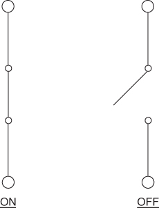
In this section, designs of planar-reconfigurable antennas are discussed. In the early days it was difficult to obtain high-end semiconductor devices commercially, so many reconfigurable antennas were made using mechanical switches, referred to more commonly as ideal switches. Such switches are ideal and have low loss, but they do not allow fast switching speed and automation. Today, with the rapid development of MEMS, semiconductor, and photoconductor technologies, most reconfigurable antennas can be fabricated easily using different diodes. A PIN diode, which can easily be made into a simple switch, has been explored extensively for designing various reconfigurable antennas because of a number of advantages, including good reliability, compact size, high switching speed, and low resistance and capacitance in the ON and OFF states. An operating PIN diode requires a dc bias, and its equivalent circuits are shown in Fig. 3.1 for both the ON (forward-biased) and OFF (reverse-biased) states. When turned on, a diode can be represented by a forward-biased resistance RS (usually, ∼ 0.1 Ω at 1 mA) and a package inductance L ( ∼ 0.1 nH). As can be seen in the figure, an OFF diode is represented by a very large reverse resistance RP and a package capacitance CT. To simplify the circuit analysis, the ON and OFF states of a diode are simply treated as ideal switches, as shown in Fig. 3.2. In the past decade, the PIN diode has been utilized in designing various frequency- and pattern-reconfigurable antennas (2–4). Although the semiconductor-made switch enables fast configuration speed, it is lossy and can seriously affect the antenna performance if not designed properly.
Figure 3.1 Equivalent circuits of a PIN diode at the ON and OFF states.
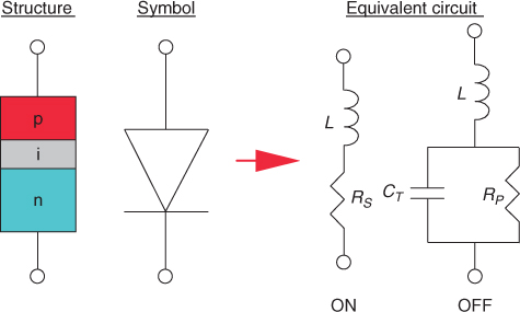
Figure 3.2 Ideal equivalent circuits of a PIN diode at the ON state (forward biased) and at the OFF state (reverse biased).
Peroulis et al. used a PIN diode to configure the operating frequency of a slot antenna (3). A transmission-line equivalent circuit was proposed to study the effect of the diode on a frequency-reconfigurable antenna. By controlling its biasing voltage, a diode can easily be turned ON and OFF. It is always very desirable to have a diode that has a low loading effect (OFF state) and low resistance (ON state). Obviously, the ON-state resistance can result in power dissipation and degrade the antenna radiation efficiency. For such a reconfigurable antenna, the total dissipated power depends on the diode's ON resistance and the number of switches being used, and these are inherent drawbacks. Analysis shows that even a small series resistance of R = 1.4 Ω can cause the antenna gain to deteriorate (2.5 dB lower than the ideal value). In simulations, a lumped resistor can be used to model the loading effect and resistance of the diode. The PIN diode can also cause the resonance frequency of the slot antenna to fluctuate, especially when more than one is employed for multifrequency operation. For the reconfigurable antenna reported in (3), it was found that the reflection coefficient is less than − 20 dB when the diode is in the OFF state. For both the ON and OFF states, the RF–dc isolation can be made better than 30 dB, with the RF–RF isolation always greater than 10 dB up to 1 GHz. The use of high-frequency diodes or RF MEMS switches can further increase the isolation for applications beyond UHF.
The performance of a reconfigurable PIN-driven slot-loaded patch antenna was compared experimentally with one made with ideal switches (4). It was found that the antenna loaded with an ON diode had a lower resonance frequency than that using an ideal switch. The reverse was seen for the antenna in the OFF state. It is worth noting that the reconfigurable antenna has very similar radiation patterns in both states. This simply implies that the diode has nearly no effect on the radiation characteristics of the antenna. A 1-dB loss of antenna gain was observed when the diode was turned on. Similar results were found by Kang et al. (2).
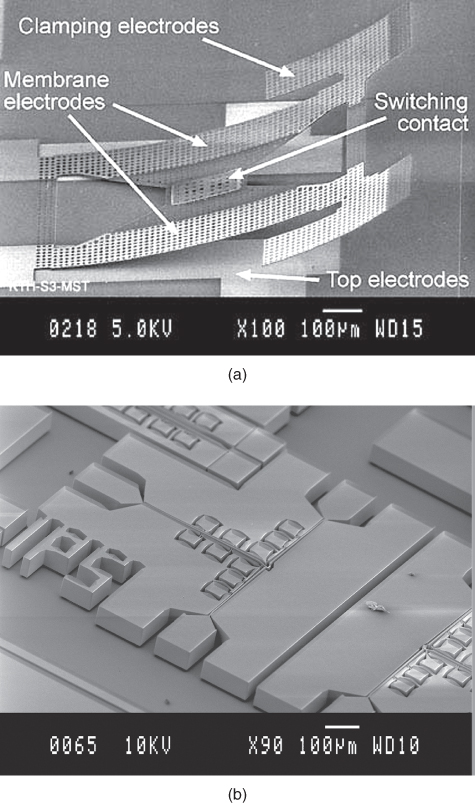
As the quality factor (Q) of the PIN diode is usually low at high frequencies (Q < 3 at 10 GHz), it has a high insertion loss and can reduce the antenna gain of a reconfigurable antenna. The use of MEMS switches, which have relatively higher Q values (Q > 10 at 10 GHz) and lower loss, can help alleviate this problem (5). Also, most MEMS devices come with a very wide operating frequency range and low power consumption. They can also be integrated monolithically with antennas and other semiconductor components. Two types of MEMS switches are shown in Fig. 3.3. Although there are still some problems, such as switching reliability and speed, the use of MEMS switches has become very common, and it is now the most feasible alternative (6) in designs of reconfigurable antennas. A single-substrate MEMS-integrated reconfigurable antenna was proposed by Jung et al. (6) to provide beam steering capability.
Figure 3.3 Two types of MEMS switches: (a) electrostatic S-shaped film switch; (b) multi-stable cantilever switch. (From http://www.ee.kth.se/php/index.php?action = research&cmd = showproject&id = 23.)
Different active devices, such as MEMS, PIN diode, and FET switches, were used by Mak et al. (7) to switch the feed port and ground of a planar inverted F antenna (PIFA). The reconfiguration performances were compared. It was found that all three active devices had a reactive loading effect on the antenna. It caused the resonance frequency of the PIFA to decrease. Also, the PIN diode was found to have the least reactive loading. All three active devices degraded the radiation efficiency of the PIFA.
Photoconducting switches were used by Panagamuwa et al. (8) to reconfigure a dipole. When it was turned off, the switch had a weak conductive effect on the antenna, causing the resonance frequency to decrease. As the photoconducting switch is transparent to electromagnetic waves, it does not disturb the antenna radiation.
Recent developments for frequency-, pattern-, and multiple-reconfigurable antennas are discussed next. Some design examples are also given.
3.3 Frequency-Reconfigurable Antennas
Frequency reconfiguration is usually accomplished by changing the operating frequency of an antenna while keeping its radiation characteristics unchanged. The operating frequency of a resonant antenna is changeable by incorporating some switches to alter the resonance length or aperture of its resonator; alternatively, it can be done by switching the feeding ports or antenna grounds (7). In past decades, many studies on frequency reconfiguration have been conducted on the slot antenna (3, 9), microstrip Yagi antenna (10), slit-loaded patch antenna (11), and slot-loaded E-shaped patch (12). Frequency-reconfigurable antennas are utilized widely in multifrequency and frequency-agile wireless systems.
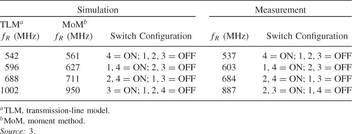
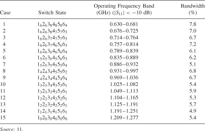
A frequency-reconfigurable S-shaped slot antenna loaded with a series of PIN diode switches was studied by Peroulis et al. (3). The configuration of the antenna is shown in Fig. 3.4. Tuning the antenna operating frequency can be done easily by changing its effective electrical length, which is controlled by the bias voltages of solid-state shunt PIN diode switches placed along the slot resonator. Here, four switches are incorporated into the slot to tune the antenna over the frequency range 540 to 950 MHz. When any of the switches is set to the ON state, the slot is shorted at that location, resulting in a decrease in the slot length and an increase in the resonance frequency. Simulations were conducted using the method of moments. The reconfigurable antenna (Fig. 3.4) was fabricated on a 100-mil-thick RT/Duroid substrate with a ground plane of 5 × 5 in2. The measured resonances of the antenna are shown in Table 3.1, together with the switch settings. Satisfactory agreement was obtained between the theoretical and experimental data. However, for the highest resonance frequency, there is a discrepancy of 13% between the transmission-line model and the measurement, and this can be attributed to the inadequacy of the equivalent circuit (for the diode) at high frequencies.
Figure 3.4 Configuration of a reconfigurable slot antenna. (From (3), copyright © 2005 IEEE, with permission.)
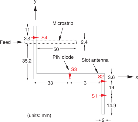
Table 3.1 Comparison of Measured and Calculated Resonance Frequencies
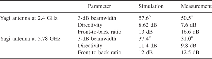
A dual-band frequency-reconfigurable Yagi antenna was studied by Wahid et al. (10). The geometry of a reconfigurable Yagi antenna is shown in Fig. 3.5. It consists of two independent Yagi antennas which are made on the same plane, switching between 2.4 and 5.78 GHz. The Yagi antenna works at 2.4 GHz when all the switches are in the ON state. The same antenna operates at 5.78 GHz when all the switches are OFF. Commercial software IE3D was used to simulate the reconfigurable Yagi antenna. With the use of ideal switches, the antenna is simulated at the ON [Fig. 3.6(a)] and OFF [Fig. 3.6(b)] states. With reference to Fig. 3.6(a), the Yagi elements have a longer electrical length when all the switches are turned on. This causes the antenna to work at 2.4 GHz. When all the switches are in the OFF state, as shown in Fig. 3.6(b), the electrical length is then truncated, causing the antenna to work at about 5.8 GHz. Without including the switches, the two antennas (Fig. 3.6) were made. The dimensions of the optimized Yagi antennas are given in Table 3.2. An RT/Duroid 5880 substrate with a thickness of 5 mils, a dielectric permittivity ε r of 2.2, and a loss tangent of 0.0009 was used for the experiments. The effect of the substrate can be omitted because of its small thickness and low loss. The measured and simulated results are compared in Table 3.3, with good agreement observed. The discrepancy between the simulated and measured results can be caused by the dielectric and conductor losses.
Figure 3.5 Dual-band reconfigurable Yagi antenna. (From (10), copyright © 2003 John Wiley & Sons, Inc., with permission.)
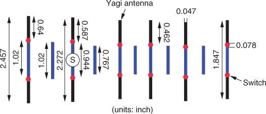
Figure 3.6 Configuration of a reconfigurable Yagi antenna: (a) ON state; (b) OFF state.
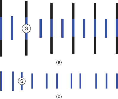
Table 3.2 Dimensions (Inches) of Yagi Antennas Optimized at 2.4 and 5.78 GHz
| Yagi Antenna at 2.4 GHz | Yagi Antenna at 5.78 GHz | |
| Length of driven element (0.42λ) | 2.272 | 0.944 |
| Length of reflector (0.499λ) | 2.457 | 1.02 |
| Length of directors (0.375λ) | 1.847 | 0.767 |
| Spacing between driven element and reflector (0.25λ) | 1.23 | 0.51 |
| Spacing between directors (0.3λ) | 1.48 | 0.61 |
Table 3.3 Comparison of Simulated and Measured Data
3.3.1 Frequency-Reconfigurable Slot-Loaded Microstrip Patch Antenna
3.3.1.1 Configuration
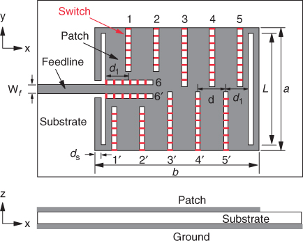
A reconfigurable microstrip-fed patch antenna was proposed for multifrequency applications by Xiao et al. (11). The configuration of the antenna is shown in Fig. 3.7. As can be seen from the figure, multiple slits are cut along the nonradiating edges of a rectangular microstrip patch to increase the electric current route on the resonator. It causes the resonance frequency to be reduced. Two pairs of short slits (slits 1–1′ and 2–2′) and three pairs of long slits (slits 3–3′, 4–4′, and 5–5′) are inserted into the two nonradiating edges of the patch. The short slits 6–6′ are used to control the impedance matching of the feedline. To have a higher level of controllability, multiple switches are incorporated uniformly into the slits. With reference to the figure, six and eight switches are used for the short and long slits, respectively. The two slits in each pair (1-1′, 2-2′, 3-3′, 4-4′, 5-5′, and 6-6′) are configured into the same state. The operating frequency of the antenna can easily be shifted by controlling the switches. For each operating frequency, good impedance matching can be obtained by manipulating the switches along the feedline (slit 6–6′).
Figure 3.7 Configuration of a frequency-reconfigurable slot-loaded microstrip patch antenna. (From (11), copyright © 2003 John Wiley & Sons, Inc., with permission.)
3.3.1.2 Results and Discussion
The simulated frequencies of a reconfigurable antenna are listed in Table 3.4. In each slit, switches are numbered from 1 to n, starting from the edge to the middle of the patch. The symbol Mn denotes a switch state in which switches from 1 to n are open (with others closed) in the Mth pair of slits. For example, M0 is a state where all the switches in the Mth pair of slits are closed. From the table it is clear that the reconfigurable antenna can shift its operating frequency over a one-octave bandwidth from 0.6 to 1.2 GHz by tuning the switches. It is worth noting that the switch settings shown in Table 3.4 are not unique. In other words, there is always more than one switch combinations that can make the antenna operate at a certain frequency. Measurements conducted by using the ideal switches are also given for some of the states. The measured and simulated results agree with each other very well. Since the operation mode for all the states in Table 3.4 is the TM10 mode, the radiating patterns are essentially unchanged for all the antenna states. Due to slit loading, the dimension of the radiating patch is decreased about 46% at 0.63 GHz compared with that of the conventional patch antenna.
Table 3.4 Frequency-Reconfigurable Characteristics of the Reconfigurable Antenna Shown in Fig. 3.7
3.3.2 Frequency-Reconfigurable E-Shaped Patch Antenna
3.3.2.1 Configuration
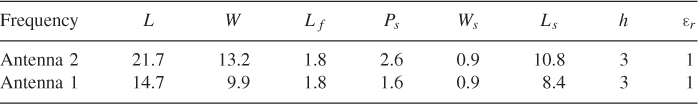
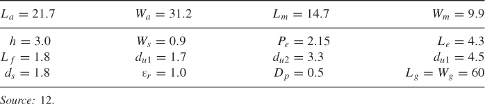
An E-shaped microstrip patch antenna, which is fed by a coaxial probe and shown in Fig. 3.8, is used to design a wideband-reconfigurable antenna. First, two similar E-shaped antennas (antennas 1 and 2) were optimized to operate at different frequencies, with their design parameters given in Table 3.5. Commercial software, HFSS 9.2, is used to simulate the characteristics of the E-shaped patches: antennas 1 and 2. The simulated VSWRs of the two antennas are shown in Fig. 3.9. As can be seen from the figure, the simulated antenna bandwidths (VSWR ≤ 2) cover 9.9 to 14.6 GHz and 7.7 to 11.3 GHz, respectively. Special care is needed for the probe-feeding position and the slit dimensions so that the two antennas can be combined easily later. A foam (with thickness hp and relative permittivity ε r = 1) is selected to support the patch. The patch is fed by a 50-Ω coaxial probe of radius Dp = 0.5 mm at the small center patch with a ground plane size (Lg × Wg) of 60 × 60 mm.
Figure 3.8 Configuration of an E-shaped patch antenna. (From (12), copyright © 2007 IET, with permission.)
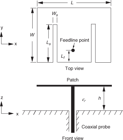
Figure 3.9 Simulated VSWRs for antennas 1 and 2. (From (12), copyright © 2007 IET, with permission.)
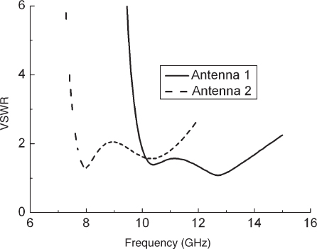
Table 3.5 Design Parameters (Millimeters) of the Two E-Shaped Microstrip Patch Antennas, One for the Lower Band and Another for the Higher
Then, with the use of 19 switches, a U-shaped patch is combined with three other rectangular patches to build a reconfigurable antenna that is switchable in two frequencies. The configuration is shown in Fig. 3.10. The design parameters are provided in Table 3.6. When all the shaded switches (with all the black switches in the OFF state) are turned on, the shape of the patch approximately equates to that for antenna 1, as can be seen from Fig. 3.11(a). On the other hand, the patch looks like antenna 2 when all the black switches are in the ON state [Fig. 3.11(b) with all the shaded switches turned OFF].
Figure 3.10 Configuration of a reconfigurable E-shaped patch antenna. (From (12), copyright © 2007 IET, with permission.)
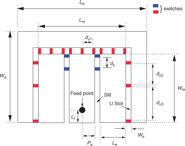
Figure 3.11 Shape of an E-shaped patch for two switch conditions: (a) all shaded switches ON (all black switches OFF); (b) all black switches ON (all shaded switches OFF).
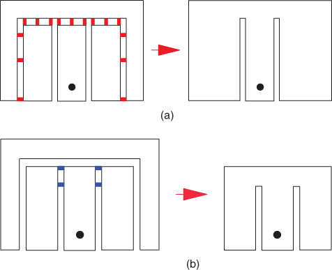
Table 3.6 Optimized Design Parameters (Millimeters) of a Reconfigurable E-Shaped Patch
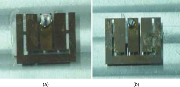
Ideal PIN diodes are used in all the simulations and measurements. In this case, the diode was simply replaced by a metallic pad (0.3 × 0.9 mm2). This is very useful for proof of concept. Of course, an actual PIN diode introduces additional losses and loading effects. Two E-shaped patch antennas were fabricated to resemble the two situations of the reconfigurable antenna; they are shown in Fig. 3.12. A copper plate with a thickness of 0.3 mm is selected to obtain good mechanical solidity. Some foam pieces with a relative permittivity of about 1 are used to support the patch. Figure 3.12(a) depicts a reconfigurable antenna where all the shaded switches are turned ON (all the black switches are OFF); whereas Fig. 3.12(b) is the antenna configuration with all the black switches turned ON (all the shaded switches are OFF).
Figure 3.12 Reconfigurable E-shaped patch antennas: (a) all shaded switches ON (all black switches OFF); (b) all black switches ON (all shaded switches OFF).
3.3.2.2 Results and Discussion
The simulated and measured VSWRs for two E-shaped patch antennas are shown in Fig. 3.13. In Fig. 3.13(a), the small patch (with all the black switches turned OFF and all the shaded switches turned ON) has three measured resonances at 9.3, 11.4, and 13.5 GHz, covering an impedance bandwidth (VSWR ≤ 2) of 38% (9.2 to 15 GHz). Figure 3.13(b) shows that the big patch (with all the black switches turned ON and all the shaded switches turned OFF) has two measured resonances at 7.8 and 9.8 GHz, with a bandwidth of 35% (7.5 to 10.7 GHz). For both cases, the discrepancy between simulation and measurement can be caused by mechanical tolerances. It was found by simulations that the width of the U-shaped slot and the positions of the diodes along the slot do not greatly affect antenna performance. Figures 3.14 and 3.15 show the simulated and measured radiation patterns of the second and third resonances (12.2 and 13.5 GHz) for the case when all the shaded switches are ON and all the black switches are OFF. The first mode is similar to the second and is therefore omitted for brevity. Figures 3.16 and 3.17 give the simulated and measured radiation patterns of the first and second resonances (8 and 10.3 GHz) when all the shaded switches are OFF and all the black switches are ON. In general, good agreement between simulation and measurement is obtained for all cases.
Figure 3.13 Simulated and measured VSWRs of a reconfigurable antenna with (a) all the shaded switches turned ON (all the black switches are OFF); (b) all the black switches turned ON (all the shaded switches are OFF). (From (12), copyright © 2007 IET, with permission.)
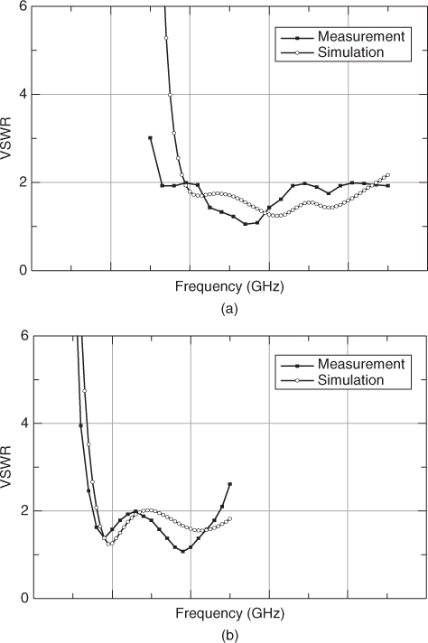
Figure 3.14 Simulated and measured normalized radiation patterns at 12.2 GHz (with all the shaded switches ON and all the black switches OFF): (a) xz-plane; (b) yz-plane. (From (12), copyright © 2007 IET, with permission.)
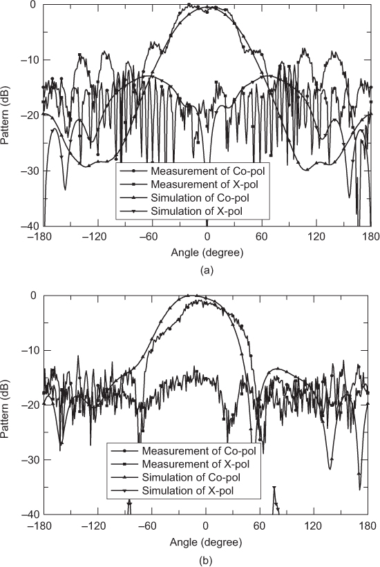
Figure 3.15 Simulated and measured normalized radiation patterns at 13.5 GHz (with all the shaded switches ON and all the black switches OFF): (a) xz-plane; (b) yz-plane. (From (12), copyright © 2007 IET, with permission.)
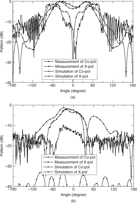
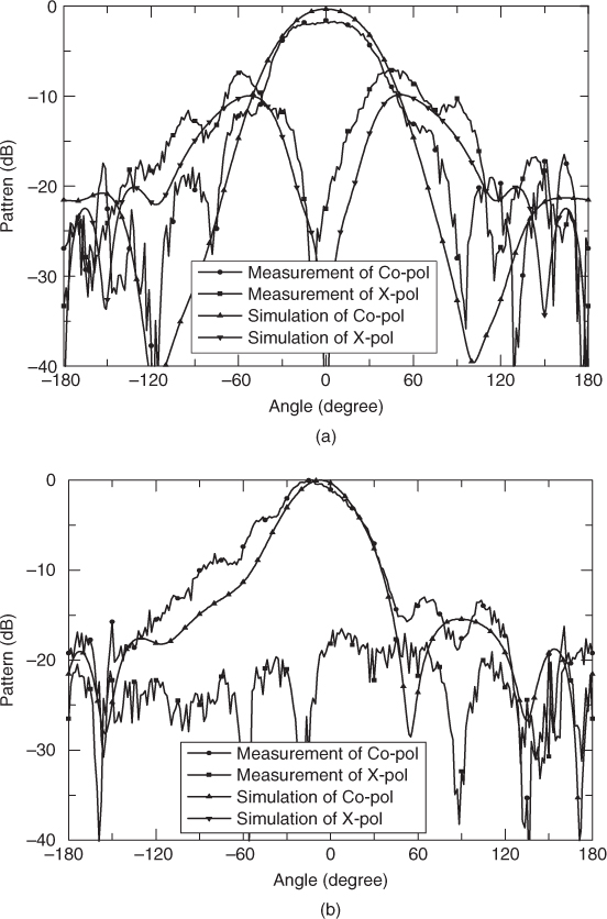
Figure 3.16 Simulated and measured normalized radiation patterns at 8 GHz (with all the shaded switches OFF and all the black switches ON): (a) xz-plane; (b) yz-plane. (From (12), copyright © 2007 IET, with permission.)
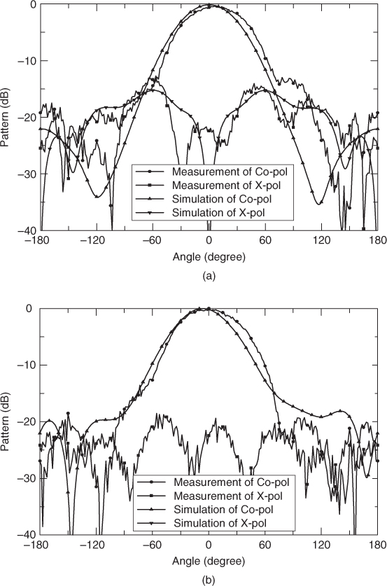
Figure 3.17 Simulated and measured normalized radiation patterns at 10.3 GHz (with all the shaded switches OFF and all the black switches ON): (a) xz-plane; (b) yz-plane. (From (12), copyright © 2007 IET, with permission.)
3.4 Pattern-Reconfigurable Antennas
A pattern-reconfigurable antenna is an EM radiator whose radiation patterns are changeable by switches. Usually, the operating frequency of such an antenna is kept constant. But in some cases it is designed to have different radiation patterns at different frequencies. Pattern reconfigurability enables wireless communication systems to avoid noisy environments, maneuver away from electronic jamming, and save energy by redirecting signals toward intended users only. Pattern-reconfigurable antennas are frequently used to increase the channel capacity and broaden the coverage area of a wireless system. Much work in past decades has been dedicated to studying pattern reconfigurable antennas. In 2003, Huff et al. (13) demonstrated a single-turn square-spiral microstrip antenna that can perform frequency and pattern reconfigurations simultaneously. Wu et al. (14) presented a pattern-reconfigurable microstrip patch antenna that has four switchable directional quasi-conical beams in different quadrants. To obtain higher antenna gain, Zhang et al. (15) and Yang et al. (16) introduced the Yagi–Uda pattern-reconfigurable microstrip parasitic arrays. For millimeter-wave applications, Xiao et al. (17, 18) presented a novel co-planar-waveguide leaky-wave antenna with pattern reconfigurability.
Pattern reconfiguration can also be accomplished by combining different antennas on a common structure (2). In this case, different radiation patterns are usually excited simultaneously by altering the radiation aperture or by changing the feeding ports. Adding, removing, and shorting some parts of a radiation aperture are among the commonly used techniques (6, 19). For such antennas it is always very desirable to have a symmetrical radiation pattern. As a result, radiation elements that have a symmetrical radiation aperture with a constant resonance frequency are preferable for designing pattern-reconfigurable antennas (15, 19).
In this section, two design examples are examined. The first pattern-reconfigurable antenna is made on a fractal patch. In the second case, a traveling-wave antenna is made reconfigurable to achieve a narrow beamwidth and a wide scan range. Here, the beam directions can be scanned continuously by changing the period of the radiation element.
3.4.1 Pattern-Reconfigurable Fractal Patch Antenna
3.4.1.1 Configuration
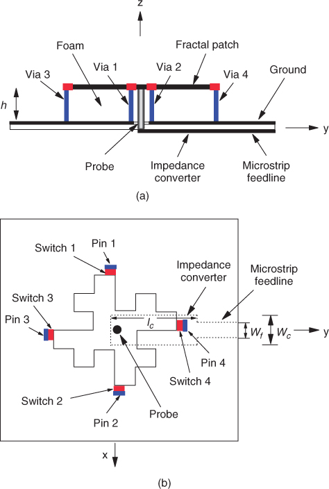
The fractal patch antenna was introduced by Yeo and Mittra in 2001 (20). A compact and pattern-reconfigurable square fractal loop was later proposed by Elkaruchouchi and El-Salam (21). Figure 3.18 shows a first-iteration fractal shape that is built by combining a square and an indentation. Such a geometry is then employed in designing the pattern-reconfigurable planar microstrip fractal antenna (19) shown in Fig. 3.19. It has a top fractal patch and a metal ground plate. The top patch is 15 × 15 mm, the indentation width in the fractal generator is 2.5 mm, and the metal ground plate is 30 × 30 mm. The top square fractal patch area of the antenna is smaller than 0.5λ × 0.5λ at 8.4 GHz. Four shorting pins are used to short the patch at four locations. One end of the pin is soldered to the ground and the other is connected by a switch to the edge of the fractal patch. Each shorting pin has dimensions of 1 × 0.5 × 4 mm. The gap between the switch and the patch is 0.5 mm. The feedline consists of a vertical probe, a λ/4 microstrip impedance convertor, and a 50-Ω microstrip feedline. A vertical probe with a diameter of 1.27 mm is used to feed the patch through a gap of 0.15 mm, which is used to introduce capacitive coupling for better impedance matching. The vertical probe is connected to a λ/4 microstrip impedance convertor and a feedline, which are etched under the ground plate. A hole with diameter of 2 mm is milled on the ground plate to prevent the probe from touching the ground plate. In the experiment, a few foam boards ( ε r ∼ 1) were used to support the patch and probe. The substrate under the ground plate has a thickness of 0.5 mm and a dielectric constant of ε r = 2.2. Referring to Fig. 3.19, other parameters of the antenna are given as follows: h = 4 mm, lc = 8.5 mm, Wc = 3.5 mm, and Wf = 1.6 mm.
Figure 3.18 First-iteration square fractal shape.
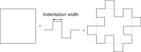
Figure 3.19 Configuration of a pattern-reconfigurable planar fractal antenna with switches: (a) front view; (b) top view.
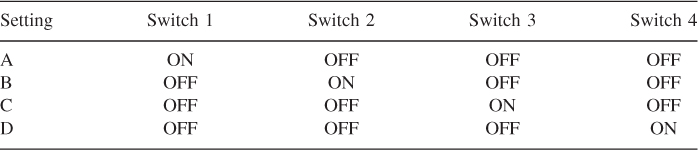
By switching the four switches ON and OFF, the antenna can be set into four symmetrical settings. Each has only one switch turned ON. For ease of description, the switches are labeled numerically (1, 2, 3, and 4). Four groups of experiments (settings A, B, C, and D) are summarized in Table 3.7. For settings A and B, the xz-plane is designated as the E-plane as well as the scanning plane; the yz-plane is the H-plane. Similarly, for settings C and D, the yz-plane is the E-plane and also the scanning plane; the xz-plane is the H-plane.
Table 3.7 Switch Settings of a Pattern-Reconfigurable Fractal Antenna
3.4.1.2 Results and Discussion
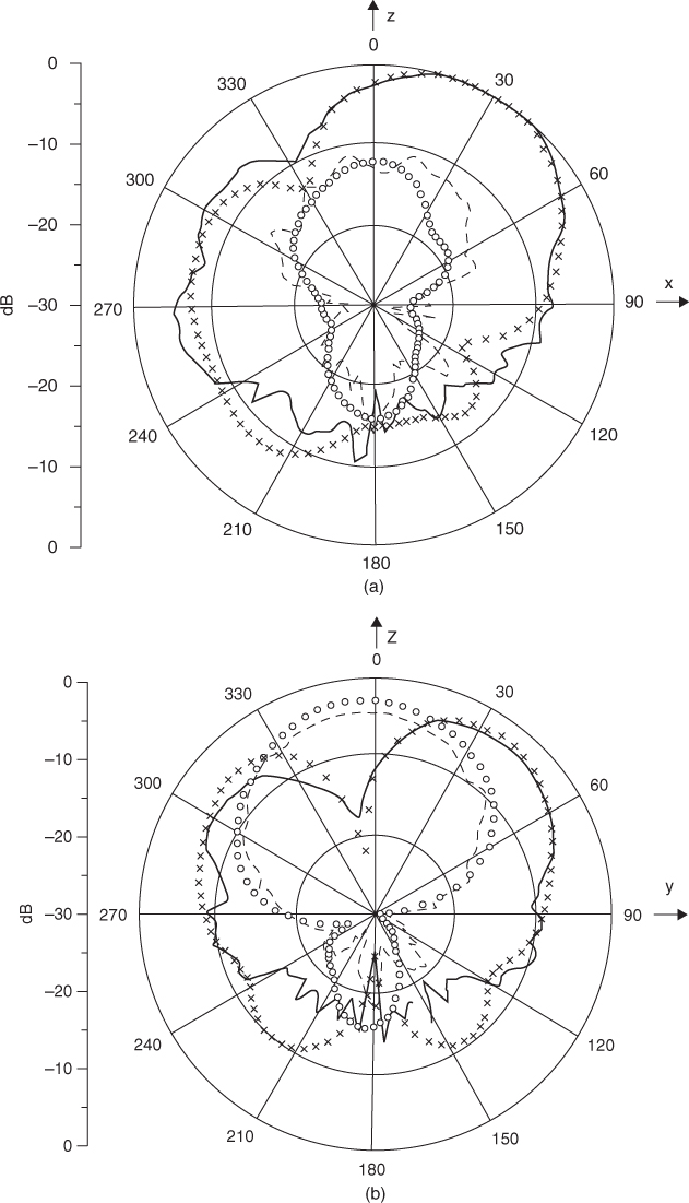
Ansoft HFSS was used to simulate the antennas. For proof of concept, all the switches are replaced by copper pads (with an area of 1 × 0.5 mm) in both the simulations and measurements. Figure 3.20 shows the simulated and measured reflection coefficients in setting B. As can be seen from the figure, the measured resonance frequency of the fractal patch is about 8.4 GHz, with a measured impedance bandwidth of about 10%. The simulated result is very close to the measurement. Due to symmetry, all four antenna settings have almost the same reflection coefficient. In Fig. 3.21, the simulated and measured radiation patterns are given in the E(xz)- and H(yz)-planes. In the xz-plane, the antenna provides a half-power beamwidth ranging from 0 to 60° at an operating frequency of 8.4 GHz. Because of its symmetry with respect to the yz-plane, the radiation pattern at setting A has a half-power beamwidth covering 300 to 360° in the xz-plane. Similarly, settings C and D, respectively, provide half-power beamwidths of 300 to 360° and 0 to 60° in the yz-plane. As can be seen from Fig. 3.21, the sidelobes and cross-polarized fields of the four settings are less than − 6 and − 10 dB, respectively. The simulated antenna gain is 4.29 dBi. If practical PIN diodes and RF MEMS devices are used for this application, the antenna gain can worsen at most by 1 dB at 8.4 GHz.
Figure 3.20 Simulated and measured reflection coefficients of a pattern-reconfigurable antenna in setting B. (From (19), copyright © 2007 IEEE, with permission.)
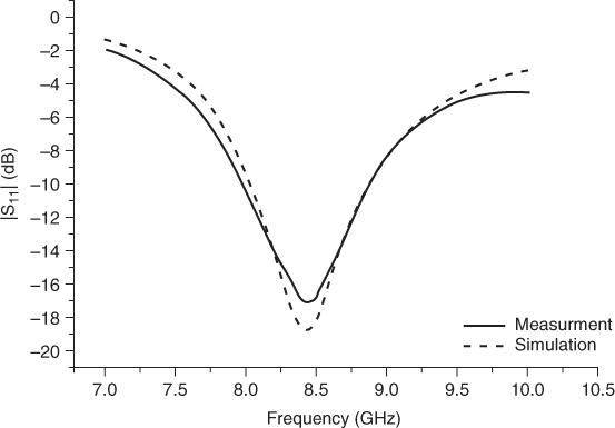
Figure 3.21 Simulated and measured radiation patterns of a pattern-reconfigurable antenna (setting B) at 8.4 GHz: (a) E-plane; (b) H-plane. (From (19), copyright © 2007 IEEE, with permission.)
3.4.2 Pattern-Reconfigurable Leaky-Wave Antenna
3.4.2.1 Configuration
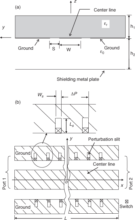
Leaky-wave antennas are very popular because of a number of advantages, such as high directivity and compact size. In this section a pattern-reconfigurable co-planar waveguide (CPW) leaky-wave antenna is presented for millimeter-wave applications (17, 18). The configuration of a leaky-wave antenna is shown in Fig. 3.22. The longitudinal direction of the periodic structure is along the x-axis, and the design parameters are selected as follows: W = 0.5 mm, S = 0.3 mm, h1 = 0.794 mm, h2 = 2 mm, Ls = 0.6 mm, Ws = 0.2 mm, ΔP = 0.4 mm, and ε r = 6.0. The entire length of the antenna is L = 50 mm. Here, 125 pairs of perturbation slits (with a distance of ΔP) are etched on the inner edges of ground planes, aligned symmetrically with the origin O. One switch is installed at the open end of each perturbation slit. A perturbation period P = p × ΔP (p is a positive integer) can be obtained by setting all p switches opened, with all others closed.
Figure 3.22 Configuration of a CPW pattern-reconfigurable antenna: (a) cross-sectional view; (b) CPW plane view. (From (18), copyright © 2005 IEEE, with permission.)
When the antenna is fed by port 1, the beam angle θm (the angle between the z-axis and the direction vector) of a spatial fast-wave component in the E-plane (xz-plane) is determined by (17)
where, λ0, k0, m, βx0, and P are the free-space wavelength, the free-space wavenumber, the order of the spatial fast wave, the phase constant of the fundamental spatial harmonic inside the periodic structure, and the perturbation period, respectively. According to eq. (3.1), θm of the spatial fast wave can be adjusted by changing the perturbation period P. Therefore, by properly adjusting the states of switches in the slits to alter the perturbation period P, the antenna pattern can scan in the E-plane. For a certain period P and a single fixed frequency f0, if βx0 is known, θm can be obtained from eq. (3.1). By combining the FDTD method with Floquet's theorem, the phase constant βx0 can easily be determined.
3.4.2.2 Results and Discussion
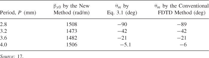
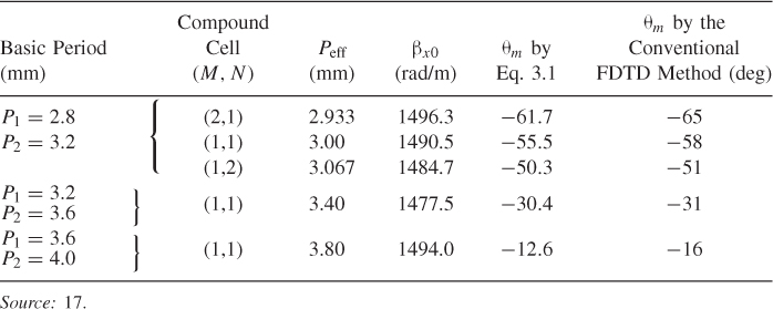
Four antenna settings with uniform periods of P = 2.8, 3.2, 3.6, and 4.0 mm, which correspond, respectively, to the open-switch settings of 7, 8, 9, and 10 switches, are selected to reconfigure the pattern. When the antenna is fed by port 1, the single main beam direction θm(m = 1) of the four settings can be predicted by eq. (3.1), and they are given in Table 3.8. From the table it can be seen that the single beam angle θm of the leaky-wave antenna can be changed within the range − 90 to 0. However, a small-angle step scan cannot be achieved using only four uniform periods. A mixed-period structure is constructed to reduce the scanning angle step by cascading compound cells. The compound cell is formed by serially connecting the M cells with a period of P1 and the N cells with a period of P2.
Table 3.8 Electromagnetic Parameters of the Multi-reconfigurable Antenna Shown in Fig. 3.22
The equivalent period of the mixed-period structure can be calculated from the equation
3.2 ![]()
where P1 − P2 ≤ min(P1, P2). The phase constant of the mixed-period structure can be calculated by linear interpolation using βx0 of the two basic uniform periodic structures that compose the mixed-period structure. Once Peff and the phase constant are obtained, the main beam angle θm of the mixed-period structure can be calculated using Eq. (3.1) (m = 1). Table 3.9 shows the results of some mixed-period states of this reconfigurable leaky-wave antenna. Results obtained using the conventional FDTD method (18) are also given in the table.
Source: (17).
Table 3.9 Electromagnetic Parameters of Some Mixed-Period States of the Pattern-Reconfigurable Antenna Shown in Fig. 3.22
When the antenna is fed by port 1, but port 2 is loaded with a matched impedance, the single beam can scan from − 90 to − 1° by combining four uniform periodic states and five mixed periodic states. Due to the symmetry of the antenna structure, when the antenna is fed by port 2, the single beam can scan from 1 to 90° by using the nine states noted above.
3.5 Multi-reconfigurable Antennas
Configuration
A multi-reconfigurable antenna can change more than one of its parameters such as frequency, pattern, polarization, and others. The ability to operate at different frequencies is highly desirable for cell phone and other wireless communication systems, which are required to work simultaneously at different standards. Pattern and polarization reconfigurations are frequently used to increase the channel capacity of a wireless system so that more users can share the same spectrum at the same time.
A Yagi–Uda antenna is able to provide both broad-side and end-fire radiation patterns. By introducing some slots and slits on its patch elements, a microstrip Yagi patch antenna was designed for frequency and pattern reconfigurations (22). This antenna is shown in Fig. 3.23, with its detailed configuration depicted in Fig. 3.24. It can be made to radiate in different directions at different frequency bands. The antenna consists of a driven patch and four parasitic patch elements. For a Yagi–Uda antenna, a parasitic element can be made a director if it is smaller than the driven element; otherwise, it functions as a reflector. All of them are square metal patches printed on a grounded substrate, with dimensions of 50 × 20 × 1 mm and a dielectric permittivity of 3. The driven element is 8 × 8 mm, approximately half the size of the guided wavelength at a resonance frequency of 9.5 GHz. According to the principle stated by Huang and Densmore (23), the dimension ratio of the director and driven elements should be made 0.8 to 0.95. All the parasitic elements have a uniform size of 7 × 7 mm, which is about 0.875 times that of the driven patch. The gaps between neighboring patches have the same distance: 0.8 mm. A 50-Ω coaxial probe is soldered along the array axis, with a distance of 1.7 mm away from the antenna center.
Figure 3.23 Multi-reconfigurable antenna. (From (22), copyright © 2008 John Wiley & Sons, Inc., with permission.)
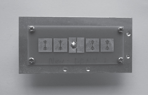
Figure 3.24 Frequency- and pattern-reconfigurable slot-loaded Yagi patch antenna: (a) antenna configuration; (b) driven patch in two frequency modes; (c) parameters of the slot: w = 0.4, a = 2, b = 0.4, c = 3.6, d = 5.2, a1 = 1.6, b1 = 0.4, c1 = 2, and d1 = 2.8 (units: mm); (d) three settings of the parasitic patch. The black squares are closed switches. (From (22), copyright © 2008 John Wiley & Sons, Inc., with permission.)
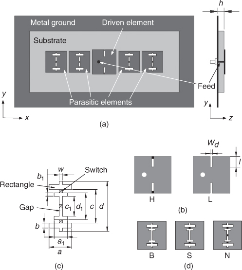
As can be seen from Fig. 3.24(a), two uniform slits are etched along the nonradiating edges of the driven patch, with a switch installed at the open end of each slit. As is well known, slits cause the resonance frequency to decrease. In this study, the slit has a length l of 2.3 mm and a width wd of 0.4 mm, as shown in Fig. 3.24(b). The driven patch can be configured to have two different resonance frequencies by opening or closing the switches. When both switches are open, the antenna mode is termed the L mode. In this case, the resonance frequency (fdl) of the driven patch decreases significantly. When both switches are closed, the antenna operates in the H mode. Now, the resonance frequency (fdh) of the driven patch decreases slightly, with fdh > fdl.
With reference to Fig. 3.24(c), a complex slot is etched on each parasitic patch to introduce extra inductance and capacitance. Also, three switches are installed along each slot to adjust the capacitance and inductance values. Three parasitic patch settings, B, S, and N, shown in Fig. 3.24(d), can be obtained. At setting B, all switches are open and the resonance frequency of the parasitic patch is much reduced. At setting S, only the middle switch is open; the others are closed. In this case, the resonance frequency of the parasitic decreases slightly. At setting N, all the switches are closed and the resonance frequency remains almost constant. The resonance frequencies of the parasitic element at these settings are called fpb, fps, and fpn, respectively, and we have fpb < fps < fpn. When it is in the H mode, the antenna settings are as follows:
- At setting B, the resonance frequency of the parasitic patch decreases, and it is lower than that of the driven patch: fpb < fdh. In this case, it acts as a reflector in the Yagi–Uda antenna.
- At setting S or N, the resonance frequency of the parasitic patch is still higher than that of the driven patch, and we have fpn > fps > fdh. The parasitic patch acts as a director.
As no matching network is used when the antenna operates in the L mode, good impedance matching can only be obtained only if the resonance frequencies of the driven patch and the B parasitic element are close to each other. The roles of the parasitic elements are described as follows:
- At setting B, the resonance frequency of the parasitic element is higher but very close to that of the driven patch: fpb > ≈ fdl. The parasitic patch acts as a director.
- At setting S or N, the resonance frequency of the parasitic element is much higher than that of the driven patch. Thus, it has a very weak directive effect on the radiation pattern.
3.5.1.1 Results and Discussion
By adjusting the settings of the parasitic patches, an antenna can be reconfigured in many different ways. When the parasitic patches on one side of the driver are directors while those on the other side are all reflectors, the main beam of the radiation pattern will tilt away from the broad side to the directors' side. When all the parasitic patches are directors or reflectors, a broad-side pattern can be obtained.
When the antenna operates in the H mode, by switching among the three configurations, the main beam of the antenna can cover a large continuous range in the upper half-space. When the antenna is in the L mode, by switching between two configurations, a large continuous beam coverage can also be achieved.
The simulated data for different settings of a pattern-reconfigurable antenna are compared in Table 3.10. For ease of description, the patches are labeled from left to right [refer to Fig.3.24(a)]. The summary of all settings, along with their simulated results, are also given in the table. The directivities and beamwidths of the H and L modes are obtained at 9.31 and 8.175 GHz, respectively. In this work, a metal pad 0.5 × 0.5 mm2 is used to model the real switch for proof of concept.
Table 3.10 Simulated Data for the Five Configurations of the Multi-reconfigurable Antenna Shown in Fig. 3.24
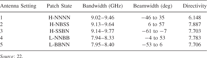
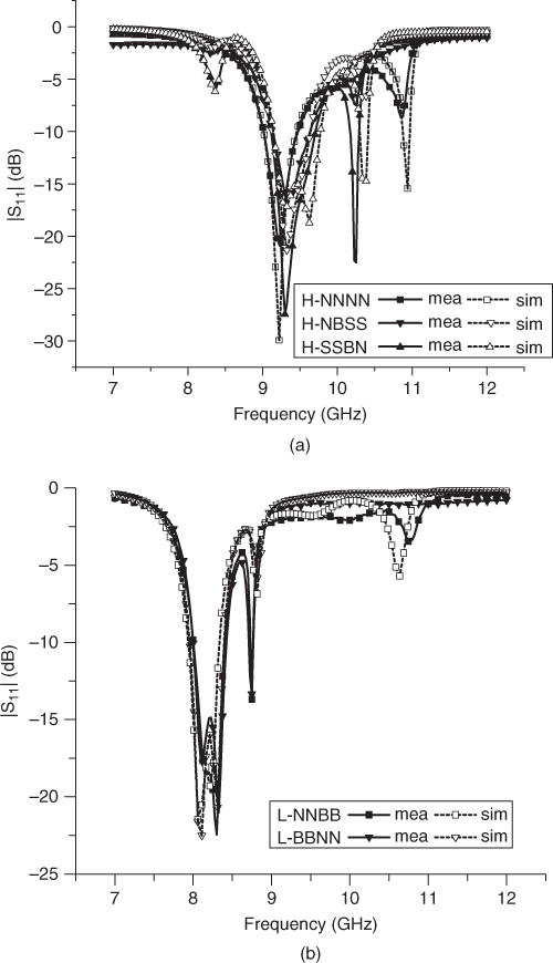
The measured and simulated S parameters of the five configurations are shown in Fig. 3.25. Settings 1, 2, and 3, which belong to the H mode, cover an impedance passband (|S11| ≤ − 10 dB) of 9.13 to 9.48 GHz; settings 4 and 5, which belong to the L mode, have a passband of 8.0 to 8.35 GHz. Simulated results show that the shared passband of settings 1, 2, and 3 is 9.14 to 9.46 GHz, and that for settings 4 and 5 is 7.95 to 8.33 GHz. The measured and simulated results agree well with each other.
Figure 3.25 Simulated and measured S parameters of five settings: (a) H mode; (b) L mode. (From (22), copyright © 2008 John Wiley & Sons, Inc., with permission.)
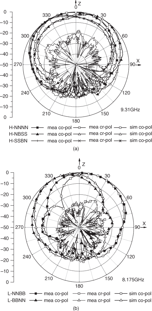
The measured radiation patterns of the three H modes and two L modes at their central frequencies (9.31 and 8.175 GHz) are shown in Fig. 3.26. The main beams of settings 1, 2, and 3 cover a continuous angular range from − 71 to + 61° in the E-plane in the upper half-space. The two lower-frequency modes of settings 4 and 5 can make the radiation pattern cover a continuous radiation range from − 56 to + 56° in the E-plane.
Figure 3.26 Measured and simulated radiation patterns in the E-plane of an antenna: (a) H mode; (b) L mode. (From (22), copyright © 2008 John Wiley & Sons, Inc., with permission.)
3.6 Conclusions
In this chapter, several frequency-, pattern-, and multi-reconfigurable antennas have been discussed. Some recent work done by researchers at the Institute of Applied Physics, University of Electronic Science and Technology of China, Chengdu, has been presented. Here, both resonating and leaky-wave antennas are deployed for designs of various reconfigurable antennas. Recent developments and issues have been described. Obviously, the development of reconfigurable antennas is always tied up with the improvement of semiconductor switches and diodes, which are used broadly to perform various antenna reconfigurations. With the availability of low-loss switches, the performance of reconfigurable antennas has been improved significantly over the past few years.
References
1. D. H. Schaubert, F. G. Farrar, S. T. Hayes, and A. Sindoris, “Frequency-agile, polarization diverse microstrip antennas and frequency scanned arrays,” U.S. patent H01Q 001/38, 4367474, Jan. 4, 1983.
2. W. S. Kang, J. A. Park, and Y. J. Yoon, Simple reconfigurable antenna with radiation pattern, Electron. Lett., vol. 44, no. 3, pp. 182–183, 2008.
3. D. Peroulis, K. Sarabandi, and L. P. B. Katehi, Design of reconfigurable slot antennas, IEEE Trans. Antennas Propag., vol. 53, pp. 645–654, Feb. 2005.
4. F. Yang and Y. Rahmat-Samii, Patch antenna with switchable slot (PASS): dual-frequency operation, Microwave Opt. Tech. Lett., vol. 31, no. 3, pp. 165–168, Nov. 2001.
5. G. M. Rebeiz, RF MEMS Theory, Design, and Technology. Hoboken, NJ: Wiley, 2003.
6. C. W. Jung, M.-J. Lee, G. P. Li, and F. De Flaviis, Reconfigurable scan-beam single-arm spiral antenna integrated with RF-MEMS switches, IEEE Trans. Antennas Propag., vol. 54, pp. 455–463, Feb. 2006.
7. A. C. K. Mak, C. R. Rowell, R. D. Murch, and C.-L. Mak, Reconfigurable multiband antenna designs for wireless communication devices, IEEE Trans. Antennas Propag., vol. 55, pp. 1919–1928, July 2007.
8. C. J. Panagamuwa, A. Chauraya, and J. C. Vardaxoglou, Frequency and beam reconfigurable antenna using photoconducting switches, IEEE Trans. Antennas Propag., vol. 54, pp. 449–454, Feb. 2006.
9. K. C. Gupta, J. Li, R. Ramadoss, C. Wang, Y. C. Lee, and V. M. Bright, Design of frequency-reconfigurable rectangular slot ring antennas, IEEE Antennas and Propagation Society International Symposium, no. 1, p. 326, 2000.
10. P. F. Wahid, M. A. Ali, and B. C. DeLoach, Jr., A reconfigurable Yagi antenna for wireless communications, Microwave Opt. Tech. Lett., vol. 38, no. 2, pp. 140–141, July 2003.
11. S. Xiao, B. Z. Wang, and X. S. Yang, A novel frequency reconfigurable antenna, Microwave Opt. Tech. Lett., vol. 36, no. 4, pp. 295–297, Feb. 2003.
12. B. Z. Wang, S. Xiao and J. Wang, Reconfigurable patch-antenna design for wideband wireless communication systems, IET Microwave Antennas Propag., vol. 1, no. 2, pp. 414–419, Apr. 2007.
13. G. H. Huff, J. Feng, S. Zhang, and J. T. Bernhard, A novel radiation pattern and frequency reconfigurable single turn square spiral microstrip antenna, IEEE Microwave Guided Wave Lett., vol. 13, no. 2, pp. 57–59, Feb. 2003.
14. W. Wu, B. Z. Wang, and S. Sun, Pattern reconfigurable microstrip patch antenna, J. Electromagn. Waves Appl., vol. 19, no. 1, pp. 107–113, Jan. 2005.
15. S. Zhang, G. H. Huff, J. Feng, and J. T. Bernhard, A pattern reconfigurable microstrip parasitic array, IEEE Trans. Antennas Propag., vol. 52, pp. 2773–2776, Oct. 2004.
16. X. S. Yang, B. Z. Wang, and Y. Zhang, Pattern reconfigurable quasi-Yagi microstrip antenna using photonic band gap structure, Microwave Opt. Tech. Lett., vol. 42, no. 4, pp. 296–297, Aug. 2004.
17. S. Xiao, B. Z. Wang, X. S. Yang, and G. Wang, Novel reconfigurable CPW leaky-wave antenna for millimeter wave application, Int. J. Infrared Millimeter Waves, vol. 23, pp. 1637–1648, Nov. 2002.
18. S. Xiao, Z. Shao, M. Fujise, and B. Z. Wang, Pattern reconfigurable leaky-wave antenna design by FDTD method and Floquet's theorem, IEEE Trans. Antennas Propag., vol. 53, pp. 1845–1848, May 2005.
19. W. Wu, B. Z. Wang, X. S. Yang, and Y. Zhang, A pattern-reconfigurable planar fractal antenna and its characteristic-mode analysis, IEEE Antennas Propag. Mag., vol. 49, no. 3, pp. 68–75, June 2007.
20. J. Yeo and R. Mittra, Modified Sierpinski gasket patch antenna for multiband applications, 2001 IEEE International Symposium on Antennas and Propagation Digest, vol. 3, pp. 134–137, June 2001.
21. H. M. Elkaruchouchi and M. N. A. El-Salam, Square loop antenna miniaturization using fractal geometry, 2003 IEEE International Symposium on Antennas and Propagation Digest, vol. 4, pp. 22–27, June 2003.
22. X. S. Yang, B. Z. Wang, S. Xiao, and K. F. Man, Frequency and pattern reconfigurable Yagi patch antenna, Microwavave Opt. Tech. Lett., vol. 50, no. 3, pp. 716–719, Mar. 2008.
23. J. Huang and A. C. Densmore, Microstrip Yagi array antenna for mobile satellite vehicle application, IEEE Trans. Antennas Propag., vol. 39, pp. 1024–1030, July 1991.