
Chapter 2
Multifunctional Passive Integrated Antennas and Components
2.1 Development of Passive Integrated Antennas and Components
In the past few decades, many advances have been reported in the development of active integrated antennas (AIAs) (1–5), which were designed by incorporating various active devices, such as an amplifier, mixer, oscillator, duplexer, or rectifier, in an antenna. Being multifunctional, an AIA integrates various signal-processing functions into an antenna to enhance the antenna bandwidth, increase the effective length of a short antenna, reduce the coupling of an array, and improve the noise factor (1, 3). Most important, such integration can help in cutting down the signal transmission path and hence reduce the chance of picking up additional electronic noise. Recently, rapid advancement in millimeter-wave technologies has drawn significant attention to the research and development of passive integrated components (PICs). In modern microwave systems it is very desirable to integrate several functions into a single module to achieve high compactness, low loss, and low cost. Generally, there are two types of multifunctional PICs, one of which combines multiple resonators to obtain multifunctionality, while another achieves multiple functions in a single resonator. In the past two decades, many multifunctional PICs, such as the antenna filter (6–11), balun filter (12–15), phase-shifter filter, antenna package (16, 17), and antenna circulator (18, 19), have been reported. In this chapter we concentrate on a discussion of the first three.
2.2 Antenna Filters
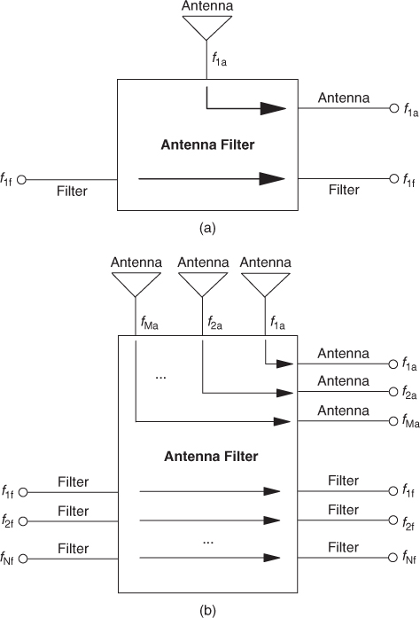
Antennas and filters are among the components that are very difficult to miniaturize, as they may require the use of resonators, which are usually bulky. The antenna filter is a newly proposed component, first reported by Lim and Leung (6), that combines the radiating and filtering elements into a single module. In general, a simple antenna filter requires at least three ports, with the simplest case shown in Fig. 2.1(a). It can easily be extended into a multiport configuration, with the signal flows as illustred in Fig. 2.1(b). This multifunctional component can be designed either with a single resonator or with a combination of multiple resonators. Designing a good antenna filter requires meeting the following criteria:
Figure 2.1 Configurations of two antenna filters: (a) three-port; (b) multiport.
Modeling an antenna filter usually requires the use of field-based simulation tools so that the coupling mechanism between the antenna and filter parts can be accounted for. In this chapter the design ideas are demonstrated using dielectric and microstrip resonators.
2.2.1 Dielectric Resonator Antenna Filter
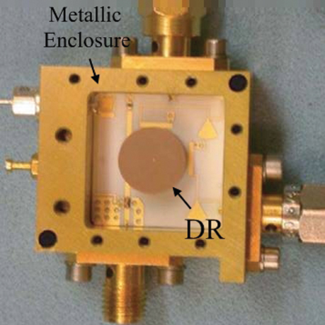
Traditionally, a dielectric resonator (DR) has been used for filter and oscillator designs because of its high Q factor (20, 21). The most distinctive advantage of a DR is that it does not have any metallic loss. A DR can be made into a variety of shapes, such as cylindrical, hemispherical, or rectangular. Some common DR examples are shown in Figs. 2.2 and 2.3. A high Q factor is very essential for achieving high frequency selectivity in a filter and low phase noise in an oscillator. The simplest excitation scheme for a DR filter (DRF) and a DR oscillator (DRO) is to use the proximity side-coupled method shown in Fig. 2.4. In designing a DRF or a DRO, an external metallic enclosure is generally used to reduce the radiation loss, at the cost of increasing the component size. A commercial DRO is shown in Fig. 2.5. Obviously, the enclosure is much larger than the DR.
Figure 2.2 Various shapes of DRs: (a) cylindrical; (b) hemispheric; (c) rectangular; (d) conical; (e) triangular; (f) annular ring.
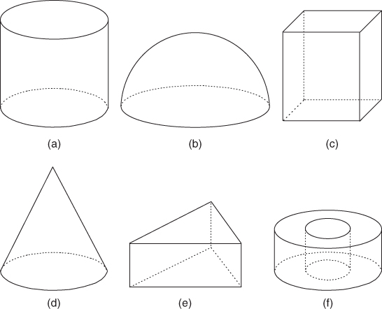
Figure 2.3 Common DR samples.
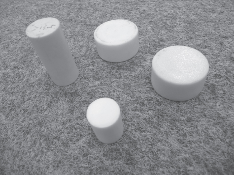
Figure 2.4 Proximity side-coupled excitation scheme for a DRF or a DRO.
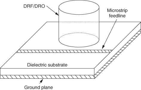
Figure 2.5 Commercial DRO.
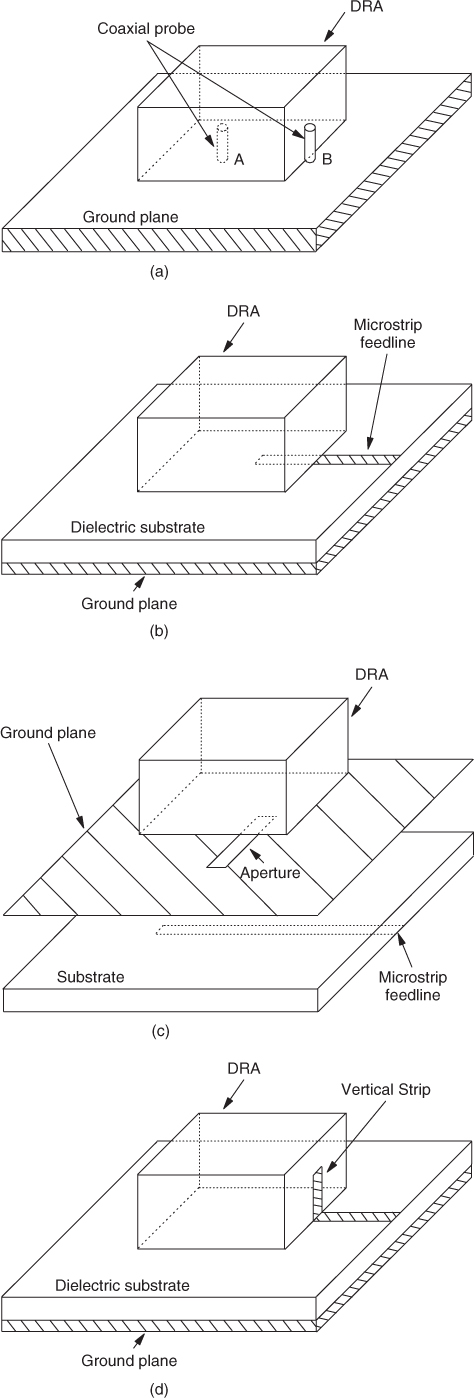
It was first shown by Long et al. in 1983 (22) that a DR could also be used as an effective antenna. Since then, the DR antenna (DRA) has received considerable attention because of a number of advantages, such as its small size, low loss, low cost, and light weight. The excitation of a DRA is very straightforward. It is worth mentioning that most of excitation methods for microstrip antennas are usually applicable to DRAs. Several popular DRA excitation schemes are displayed in Fig. 2.6. As for the coaxial-probe feeding method shown in Fig. 2.6(a), the probe can be placed either internally (position A) or externally (position B) to the DR. The metallic probe may generate extra ohmic loss and self-reactance at millimeter-wave frequencies, which are very undesirable. Also, the internal probing requires drilling a hole in the superhard DR, which is very tough in reality. As a result, the microstrip- and aperture-fed schemes [Fig. 2.6(b) and (c)] are more attractive since a DR can easily be excited simply by placing it on top of an excitation source. It is worth mentioning that the two microstrip-oriented feeding methods can easily be integrated with monolithic microwave integrated circuits. In practice, however, for all the aforementioned excitation schemes, the formation of an airgap between the DR and the ground plane is sometimes unavoidable during the manufacturing process, and it can seriously affect the coupling efficiency of the fields. To overcome this problem, the conformal-strip feeding method was proposed, in which a metallic strip is closely attached on the DR surface, as depicted in Fig. 2.6(d). Noticeably, this method shares most of the principal advantages of the coaxial-probe method.
Figure 2.6 DRA with various feeding schemes: (a) coaxial probe; (b) microstripline; (c) microstrip-fed aperture; (d) vertical strip.
In the past few years, many reports have been published on DRAs (22–24) and DRFs (25–28). Thus far, however, very little or no work has been carried out to combine a DRA and a DRF using a single piece of DR. The Q factors of the DRF and DRO are usually high, to reduce the insertion loss, but that of the DRA is usually low, to enhance the radiation and bandwidth. Because of the very different Q-factor requirements, it seems intuitively contradictory to make a DRA and a DRF using a single piece of DR. The first successful demonstration of a DRA filter (DRAF), a dual-functional device that combines an antenna and a filter in a single piece, was reported in 2008 (6). In this newly proposed dual-functional component, the antenna and filter share the same resonator. In this case, two different resonances of a resonator are used in designing the two very different functions. Use is made of the TE01δ and HEM11δ modes of the DR to design the DRF and DRA, respectively. Because of the orthogonality of the two modes, the antenna and filter parts of the DRAF can be designed and tuned separately and almost independently. It was found that the antenna and filter parts can also be designed at the same or different frequencies. A cylindrical DR loaded with a metallic disk is utilized as the resonator for the antenna as well as for the bandpass filter. A top-loading metallic disk is used to improve the insertion loss of the DRF and simultaneously, to tune the filter. It has a negligible effect on the radiation efficiency of the DRA.
2.2.1.1 Configuration
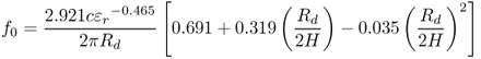
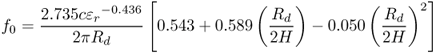
The design idea is demonstrated using a cylindrical DR with a radius Rd of 10.5 mm, a height H of 9 mm, and a dielectric constant ε r of 34. The TE01δ and HEM11δ modes of a bare cylindrical DR can be calculated using the empirical equations (2.1) and (2.2) (23).
TE01δ mode:
HEM11δ mode:
where c is the speed of light in air. The TE01δ and HEM11δ field patterns of a cylindrical DR are sketched in Fig. 2.7. When used for a DRF design with a ground plane, the DR is half-truncated (cut along the line GG′ to remove the bottom-half DR). Usually, two 50-Ω microstrips are placed adjacent to the DR to excite the magnetic field of the end-fire TE01δ mode. Similarly, a centrally placed microstrip (at the maximum electric field point) can be used to excite the broad-side HEM11δ mode in the half-volume DR for the antenna. For ease of reference, the fields of the dominant mode of a circular microstrip patch are also given in Fig. 2.7. With reference to Fig. 2.7(c), it is obvious that there are only TM modes in the patch, due to the boundary condition of the magnetic field, Hz = 0 (29, 30). Owing to this limitation, the microstrip patch cannot be used to realize this idea.
Figure 2.7 Electric and magnetic field patterns for (a) the TE01δ mode of a cylindrical DR; (b) the HEM11δ mode of a cylindrical DR; (c) the TM01 mode of a cylindrical microstrip patch antenna. (From (6), copyright © 2008 IEEE, with permission.)
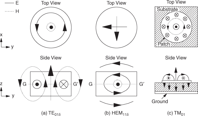
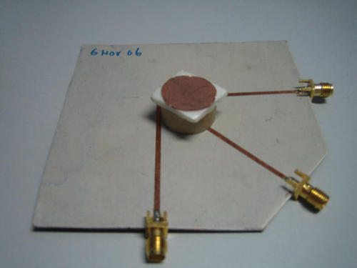
Figure 2.8 shows the configuration of the first-order DRAF, where the aforementioned DR is used. A circular metallic disk of radius Rc = 10 mm is displaced concentrically at h = 4 mm from the top of the DR. HFSS simulations show that the DRAF is working in its fundamental broad-side HEM11δ mode at 2.68 GHz (23). A DRAF prototype is shown in Fig. 2.9.
Figure 2.8 First-order cylindrical DRAF: (a) top view; (b) front view. (From (6), copyright © 2008 IEEE, with permission.)
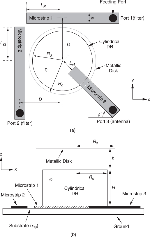
Figure 2.9 First-order DRAF.
It is well known that the fundamental end-fire TE01δ mode can be excited in a cylindrical DR when the condition Rd > H (20) is met. HFSS simulation shows that the resonance frequency of the TE01δ mode of the first-order DRAF is 3.095 GHz. In this case, two conventional 50-Ω microstrips (w = 1.99 mm) are etched orthogonally on a Duroid substrate ( ε rs = 2.94 and thickness 0.762 mm) to side-couple the DR. As can be seen from Fig. 2.8, microstrips 1 and 2 are used to excite the TE01δ mode of the DR for designing the filter part of the DRAF. The feedlines have an offset of D = 11.5 mm from the center of the DR, with matching stub lengths of Ls1 = Ls2 = 10 mm. For the antenna operation, the DR is placed on top of a feedline for excitation of the broad-side HEM11δ mode. The microstrip has a matching stub offset of Ls3 = 4.6 mm, with an inclination angle of ϕ′ = 45°.
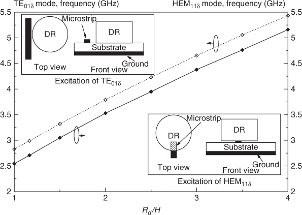
A mode chart shows the effect of a design parameter on a certain resonance. Figure 2.10 shows a simulated mode chart for the fundamental end-fire TE01δ and broad-side HEM11δ modes of a microstrip-fed cylindrical DR as a function of Rd/H, with Rd = 10.5 mm and ε r = 34. The HFSS simulation models (50-Ω microstrip feedlines, with substrate ε rs = 2.94 and thickness 0.762 mm) are also shown in the insets, where the side- and centrally coupling methods are used to excite the TE01δ and HEM11δ modes, respectively. As can be seen from the figure, the resonance frequencies of both modes increase with increasing Rd/H ratio in the frequency range 2.5 to 5.5 GHz.
Figure 2.10 Mode chart for the fundamental end-fire TE01δ and broad-side HEM11δ modes of a microstrip-fed cylindrical DR, with R = 10.5 mm. The insets show the top and side views of the HFSS simulation models. (From (6), copyright © 2008 IEEE, with permission.)
2.2.1.2 Results and Discussion
The commercial software Ansoft HFSS was used to simulate a DRAF, and measurements were carried out to verify the simulations. Usually, simulations that involve three-dimensional microwave configurations and radiation computations are done more conveniently using field-based software tools. In microwave measurements, all the unused ports were terminated by 50-Ω loads.
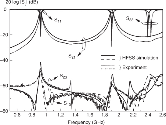
The first-order DRAF in Fig. 2.8 was studied first. The simulated and measured reflection coefficients, insertion losses, and mutual couplings between ports are shown in Fig. 2.11. The results of the filter part (DRF) of the DRAF are discussed first. As a side-coupling scheme is used for exciting the DR, it was found from simulations that a high dielectric constant is needed for efficient field coupling. A higher dielectric constant, say ε r > 20, is needed to excite the TE01δ mode efficiently. Also, it is found from simulations that the TE01δ mode cannot be excited properly when a DR of ε r = 10 is used. As can be seen from Fig. 2.11, the measured and simulated operating frequencies of the DRF are 3.054 and 3.095 GHz, respectively, with an error of 1.34%. The insertion loss measured is 2.19 dB at the operational frequency, which is slightly larger than that for simulation (1.6 dB). This can be caused by omission of the SMA connectors in the simulation. Also, for a simplified simulation model, perfect conductors and lossless dielectrics were used to simulate the feedlines and substrates. In practice, each SMA connector has an insertion loss of about 0.15 to 0.2 dB over the frequency range, and the conductor has some additional loss, which can be quite severe in millimeter-wave ranges. As can be seen in Fig. 2.11, the measured and simulated 3-dB passbands of the DRF are about 18 and 17 MHz, respectively. With reference to Fig. 2.11, both the measured and simulated reflection coefficients at port 1 (from S11) are about 16 dB at the resonance. Similar results were obtained for the reflection coefficients at port 2, which is expected because of the symmetry.
Figure 2.11 Simulated and measured reflection coefficients, insertion losses, and coupling coefficients of the first-order cylindrical DRAF (Fig. 2.8). The inset shows the simulated and measured input impedances of the DRA. (From (6), copyright © 2008 IEEE, with permission.)
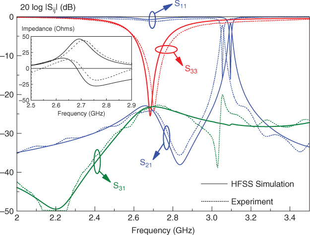
Next, the antenna (DRA) part (port 3 in Fig. 2.8) of the DRAF is analyzed. The measured and simulated resonance frequencies are given by 2.70 and 2.68 GHz (with an error of 0.74%), respectively. With reference to Fig. 2.11, the measured and simulated impedance bandwidths (S33 ≤ − 10 dB) are 3.68 and 3.35%, respectively. The measured and simulated input impedances of the DRA are shown in the inset, with good agreement observed between the simulation and the measurement. The coupling between the DRA and DRF ports (S31, S32) is in general less than −20 dB across the entire frequency range. This shows that the antenna and filter parts can be designed and tuned almost independently.
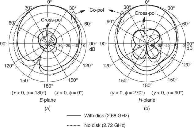
The measured and simulated radiation patterns of the antenna part (port 3 in Fig. 2.8) of the DRAF are illustrated in Fig. 2.12. The E- and H-planes are defined at the cut planes of ϕ′ = 45° and − 45°, respectively, as shown in Fig. 2.8. As can be seen from the figure, a broad-side HEM11δ mode is obtained, which is expected for the fundamental mode. In the broad-side direction (θ = 0°), the cross-polarized fields are weaker than their co-polarized counterparts by at least 20 dB. Figure 2.13 shows the measured antenna gain of the DRA as a function of frequency. It can be seen from the figure that the antenna gain is approximately 5 dBi at resonance. The measured antenna gain with the metallic disk removed is shown for comparison. It is found that the metallic disk has little effect on the antenna gain. The simulated radiation patterns for the two configurations (DRAFs with and without the metallic disk) are compared in Fig. 2.14. As can be seen from the figure, the patterns of the two configurations are quite similar. It shows that the top-loading metallic disk can be used to tune the filter and improve filter performance without greatly affecting the normal operation of the antenna.
Figure 2.12 Simulated and measured normalized radiation patterns of the first-order cylindrical DRAF (Fig. 2.8): (a) E-plane; (b) H-plane. (From (6), copyright © 2008 IEEE, with permission.)
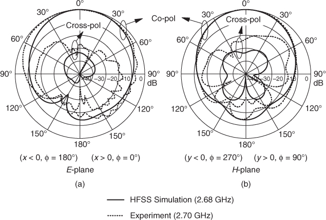
Figure 2.13 Measured antenna gains of the first-order cylindrical DRAFs in Fig. 2.8, with and without a loading metallic disk. (From (6), copyright © 2008 IEEE, with permission.)
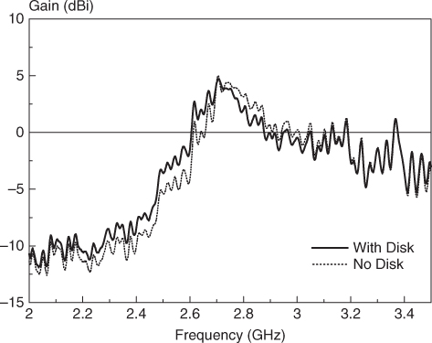
Figure 2.14 Simulated normalized radiation patterns of the first-order cylindrical DRAF in Fig. 2.8: (a) E-plane; (b) H-plane. (From (6), copyright © 2008 IEEE, with permission.)
For an antenna filter, it is very important that the antenna and the filter can be designed separately. This is possible if the coupling between the two elements is small enough. To investigate further, an isolated DRA (without the filter part) was constructed by removing microstrips 1 and 2 (in Fig. 2.8). Similarly, an isolated DRF was built by removing microstrip 3 from the DRAF. Table 2.1 compares the simulated resonance frequencies of the stand-alone DRA or DRF with those of the DRAF. As can be seen from the table, the resonance frequencies of the antenna and filter parts of the DRAF are very close to those of the stand-alone DRA or DRF. This is very encouraging, as it shows that designs of the antenna and filter parts can be done quite independently for the DRAF, due to the orthogonality of the electric fields of the TE01δ and HEM11δ modes, which can be seen clearly from Fig. 2.7(a) and 2.7(b).
Table 2.1 Comparison of Simulated Resonance Frequencies (GHz) of a DRAF and an Isolated DRA/DRF
| Antenna Frequency | Filter Frequency | |
| DRAF | 2.68 | 3.095 |
| Isolated DRA or DRF | 2.66 | 3.106 |
| (isolated DRA) | (isolated DRF) |
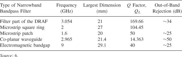
Next, we discuss the performances of the filter part of a DRAF. Table 2.2 compares the loaded Q factor (QL) and out-of-band rejection of the DRAF with those of existing bandpass filters. The QL factor is calculated using QL = f0/BW3dB, where f0 and BW3dB are the measured central operating frequency and 3-dB filter bandwidth (31), respectively. As can be seen from the table, the DRAF has a much higher Q factor than that for conventional microstrip-based bandpass filters, which have a higher conductor loss. Although the Q factor of the DRAF is much lower than for the conventional cavity-encapsulated DRF (32), the DRAF has the advantage of being more compact. The QL factor of a conventional cavity-encapsulated DRF can easily be made greater than 1000. A metallic cavity cannot be used in this case as it disturbs the antenna operation. Of course, the DRAF can be further miniaturized by increasing the permittivity, but this is not the focus here. The out-of-band-performance is found to be greater than 30 dB.
Table 2.2 Comparison of the DRAF and Existing Bandpass Filters
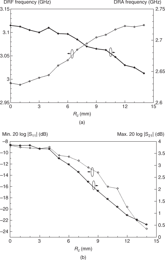
Parametric studies have been performed on the top-loading metallic disk. Figure 2.15(a) shows the effect of the height h on the operating frequencies of a DRA and a DRF. As can be seen from the figure, the DRA frequency increases from 2.65 GHz to 2.72 GHz (2.64%), and the DRF frequency decreases from 3.23 GHz to 3.00 GHz (7.12%), as h is increased from 2 to 14 mm. The effects of h on the reflection coefficients and insertion losses are shown in Fig. 2.15(b). It is obvious that both the reflection coefficients and insertion losses can be improved by using a smaller h. Figure 2.16 shows the effect of the disk radius Rc on the DRAF. As can be observed from Fig. 2.16(a), the DRA frequency decreases with, and the DRF frequency increases with, increasing Rc. As can be seen from Fig. 2.16(b), both the reflection coefficients and insertion losses can be improved by using a larger disk. Obviously, the DRAF can be fine-tuned by varying the height and radius of the metallic disk, which can be a very important feature for the filter (33, 34).
Figure 2.15 Effect of the height h of a metallic disk on the DRAF in Fig. 2.8: (a) resonance frequencies of the DRA and the DRF as a function of h; (b) minimum 20 log |S11| (maximum return loss) and maximum 20 log |S21| (minimum insertion loss) as a function of h. (From (6), copyright © 2008 IEEE, with permission.)
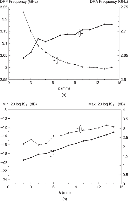
Figure 2.16 Effect of the radius Rc of a metallic disk on the DRAF in Fig. 2.8: (a) resonance frequencies of the DRA and the DRF as a function of Rc; (b) minimum 20 log |S11| (maximum return loss) and maximum 20 log |S21| (minimum insertion loss) as a function of Rc. (From (6), copyright © 2008 IEEE, with permission.)
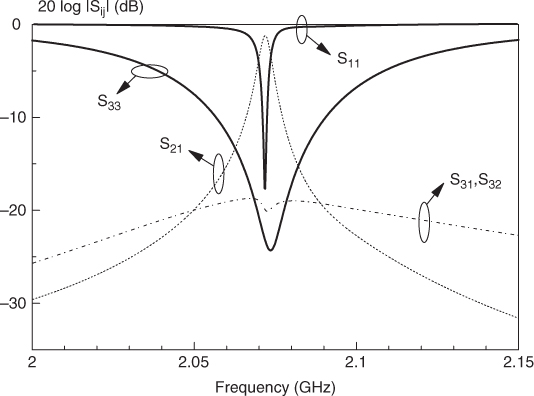
The DRAF in Fig. 2.8 has different antenna and filter operating frequencies. It will be shown that a DRAF can also be designed to have the two frequencies coincident with each other. Figure 2.17 shows the simulated results, with parameters ε r = 80, Rd = 10 mm, H = 8.8 mm, Rc = 10 mm, h = 5.2 mm, D = 11.8 mm, Ls1 = Ls2 = 10 mm, and Ls3 = 2.2 mm. It should be mentioned that although both the DRA and DRF operate at the same frequency, the coupling between them (S31, S32) is still very small, about −20 dB. This implies that the antenna and filter parts can be designed separately.
Figure 2.17 Simulated reflection coefficient, insertion loss, and coupling coefficient of a disk-loaded cylindrical DRAF shown as a function of frequency. In this case, a DRA and a DRF have the same operating frequency. (From (6), copyright © 2008 IEEE, with permission.)
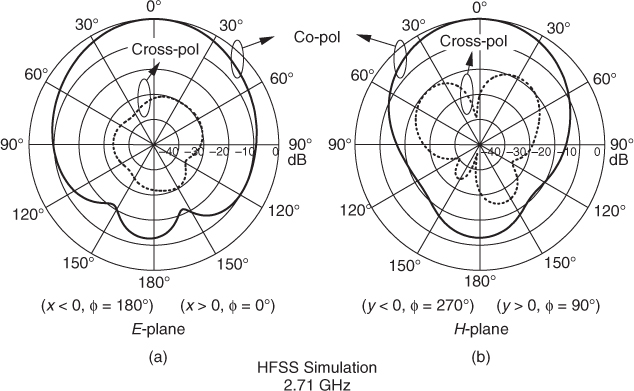
A second-order DRAF is also designed using two disk-loaded DRs, with the configuration shown in Fig. 2.18. The optimized design parameters are ε r = 34, Rd = 10.5 mm, H = 9 mm, Rc = 10 mm, h = 4 mm, D = 12 mm, d = 34 mm, Ls1 = Ls2 = 16 mm, and Ls3 = Ls4 = 4.6 mm. All of the microstrip feedlines are 50-Ω lines. Ports 1 and 2 are for the DRF, whereas ports 3 and 4 are for the DRA. Figure 2.19 shows the simulated reflection coefficients, insertion losses, and coupling coefficients of a second-order DRAF. During the tuning process, it was found that the resonance frequencies of the antenna and filter parts were almost independent of each other. This is not surprising, due to the orthogonality between the fields of the modes. Furthermore, microstrips 1 and 2 (filter ports) are normal to microstrips 3 and 4 (antenna ports), making the coupling between the microstrip lines very small. With reference to Fig. 2.19, the simulated DRA frequency at port 3 (or port 4) is 2.71 GHz, which is only slightly higher than for the first-order version. Two modes are observed for the DRF, which is expected for a dual-mode bandpass filter. The out-of-band rejection of the filter part of the second-order DRAF is much better than that of its first-order counterpart. Figure 2.20 shows the simulated E-plane (yz-plane) and H-plane (xz-plane) radiation patterns of the antenna part of the second-order DRAF. Again, the co-polarized fields are stronger than their cross-polarized counterparts by at least 20 dB in the broad-side direction. It should be mentioned that a higher-order DRAF can easily be obtained by increasing the number of DRs.
Figure 2.18 Second-order DRAF: (a) top view; (b) side view. (From (6), copyright © 2008 IEEE, with permission.)
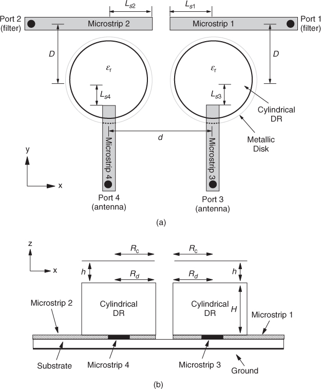
Figure 2.19 Simulated reflection coefficients, insertion losses, and coupling coefficients of the second-order DRAF (Fig. 2.18) shown as a function of frequency. (From (6), copyright © 2008 IEEE, with permission.)
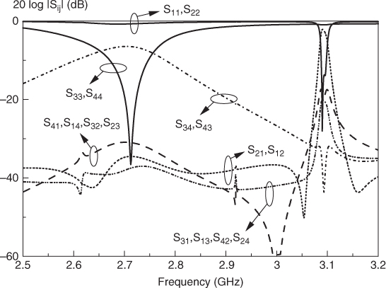
Figure 2.20 Simulated normalized radiation patterns of the second-order DRAF in Fig. 2.18: (a) E-plane; (b) H-plane. (From (6), copyright © 2008 IEEE, with permission.)
2.2.2 Other DRAFs
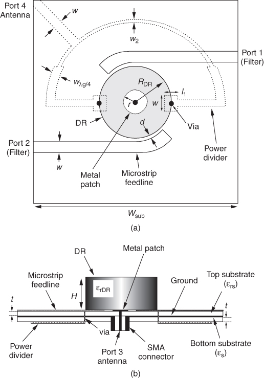
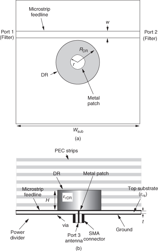
Other DRAFs have also been reported (7, 8). A dual-functional DR that works simultaneously as a diversity DRA and a bandpass DRF was reported by Hady et al. (7). The configuration is shown in Fig. 2.21. It can be seen that two resonances (TM01δ and HEM11δ) of the DR are excited at ports 3 and 4 for the antenna. At the same time, the high-Q TE01δ has been excited for a bandpass DRF at ports 1 and 2. A Trans-Tech DR with ε r, DR = 36.6, RDR = 13.27 mm, and H = 8.33 mm was used for the experiment. It is excited by a circular metallic patch being fed by the center conductor of an SMA connector, shown in Fig. 2.21. The microstrip feeding networks are built on two pieces of Duroid 6002 ( ε rs = 2.94, Wsub = 80 mm, and t = 1.524 mm) stacked bottom to bottom, with a ground plane inserted at the center. For the filter part, two curved microstrip feedlines are placed adjacent to the DR for excitation of the TE01δ mode. A power divider, placed at the bottom surface of the bottom substrate, is used to obtain the broad-side HEM11δ mode in the DRA. The TM01δ mode, being end-fire in nature, is excited by a circular metallic patch placed at the bottom of the DR. Other design parameters are w = 3.788 mm, w2 = 1.014 mm, ![]() mm, r = 6 mm, d = 1.1 mm, and l1 = 3 mm. Further information and results may be found in reference (7).
mm, r = 6 mm, d = 1.1 mm, and l1 = 3 mm. Further information and results may be found in reference (7).
Figure 2.21 Triple-mode DRAF: (a) top view; (b) front view. (From (7).)
The same excitation scheme (that was used by Hady et al. (7)) was also used for exciting the TM01δ mode in a cylindrical DR for antenna design (8). A coaxial-fed circular patch (with r = 3 mm) was used here. In the same piece of work, a conventional side-coupled microstrip was used to excite the high-Q TE01δ mode to implement a DRF. In this case the DR is placed 1.5 mm away from the edge of the microstrip to ensure efficient coupling. The configuration is shown in Fig. 2.22. The same DR and substrate were used again for this new design. A cavity (49 × 53 × 25 mm3) made of metallic strips was used to improve the insertion loss of the filter. The strips were aligned horizontally so that they were virtually invisible to the antenna mode. The horizontal strips were made on the sidewalls of a thin RT/Duroid 6002 substrate with a strip width of 3 mm and the spacing width of 2 mm (between strips). In addition, a top cover that is made of circular strips (with a strip width of 2 mm and spacing width of 3 mm) is placed on top of the cavity. Other detailed results are available in reference (8).
Figure 2.22 DRAF: (a) top view; (b) front view. (From (8).)
2.2.3 Microstrip-Based Antenna Filters
2.2.3.1 Rectangular Microstrip Ring–Patch Antenna Filter
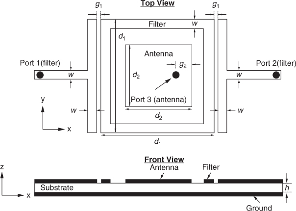
In this section a three-port antenna filter that is made on a single substrate is studied (9). By integrating the antenna and filter together, the system size can be reduced considerably. This multifunction module consists of a microstrip ring and a microstrip patch, which can be placed very close to each other. It was found that the coupling between the antenna and filter is low, so it is not necessary to use isolating ground layers. The proposed design is particularly useful for system-on-package solutions, where the antenna and filter parts are usually made separately on the top surface of a package (35–37).
Configuration
The configuration of the microstrip antenna filter proposed (9) is illustrated in Fig. 2.23, where a probe-fed rectangular patch antenna (d2 = 35 mm and g2 = 4.3 mm) is placed concentrically in the central area of a rectangular ring filter (d1 = 54 mm, w = 1.99 mm, and g1 = 0.2 mm). In this case, the filter part has a narrow bandwidth. A Duroid substrate of ε r = 2.94 and thickness h = 0.762 mm was used in the design here. Typically, the unloaded Q factor of the ring-shaped microstrip filter is about 100 (38). Since the Q factor is high, the filter response is narrowband. The ground plane of the antenna filter is 12 cm × 12 cm.
Figure 2.23 Antenna filter consisting of a rectangular microstrip patch antenna and a ring filter. (From (9), copyright © 2010 IEEE, with permission.)
Results and Discussion
Ansoft HFSS was used to study the reflection coefficient, radiation pattern, insertion loss, and mutual coupling of the antenna filter. In the measurements, each unused port was terminated with a 50-Ω load. Each configuration was fabricated on a single substrate. The simulations were verified by measurements, and good agreement between them was obtained. Figure 2.24 shows the simulated and measured reflection coefficients, insertion losses, and mutual couplings between different ports. The filter performances (ports 1 and 2) of the antenna filter are first studied. As can be seen from the figure, the measured and simulated resonance frequencies of the filter part are 930.500 and 917.375 MHz, respectively, with an error of 1.43%. The measured and simulated insertion losses are 2 and 0.082 dB, respectively. A higher loss is found in the measurement because it has included the losses of the feedlines and SMA connectors used in the experiment. With reference to the figure, the measured and simulated 3-dB passbands are 25 and 29 MHz, respectively. At port 1, the measured and simulated reflection coefficients are 15.30 and 21.27 dB, respectively. Similar results were obtained for port 2, which is expected because of the symmetry. A higher-order mode is found at 1.90 GHz, which was also reported by Chang and Hsieh (38).
Figure 2.24 Simulated and measured reflection coefficients, insertion losses, and coupling coefficients of the antenna filter shown as a function of frequency in Fig. 2.23. (From (9), copyright © 2010 IEEE, with permission.)
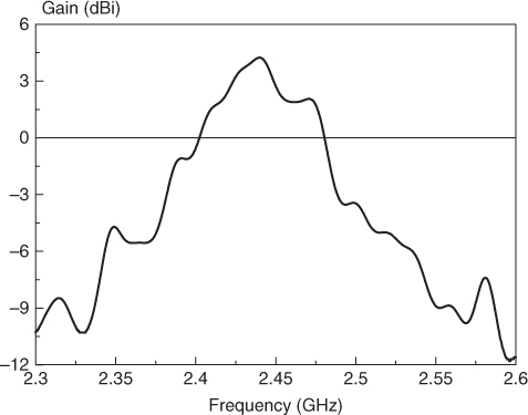
The performances of the antenna part (port 3) of the antenna filter are now addressed. The patch antenna operates in its fundamental TM01 mode. With reference to Fig. 2.24, the measured and simulated resonance frequencies are 2.437 and 2.395 GHz, respectively, with an error of 1.75%. The measured and simulated impedance bandwidths (S33 ≤ − 10 dB) are 0.81 and 0.54%, respectively. This is typical, as the Q factor for the patch resonator is usually high. It is noted from the figure that the coupling between the antenna and filter ports is generally weaker than 40 dB over the entire frequency range. This is highly desirable, as it enables the filter and antenna parts to be designed independently. The measured and simulated radiation patterns are given in Fig. 2.25. As can be observed from the figure, a broad-side mode is obtained (39), with the cross-polarized fields weaker than the copolarized fields by at least 18 dB in the bore-sight direction (θ = 0°). The measured cross-polarized fields are generally stronger than the simulated fields, due to various experimental tolerances. Referring to Fig. 2.26, the measured antenna gain is 4.24 dBi at 2.44 GHz, which is lower than that for a typical microstrip antenna.
Figure 2.25 Simulated and measured normalized radiation patterns of the antenna filter in Fig. 2.23. (From (9), copyright © 2010 IEEE, with permission.)
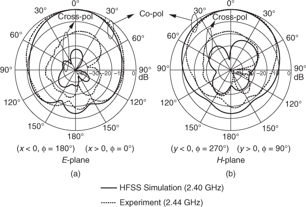
Figure 2.26 Measured antenna gain of the antenna filter in Fig. 2.23. (From (9), copyright © 2010 IEEE, with permission.)
2.2.3.2 Circular Microstrip Ring–Patch Antenna Filter
Configuration
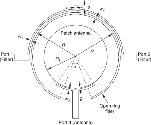
Figure 2.27 shows a microstrip antenna filter that is designed by combining a circular patch and an open-ring resonator (10) into a single resonator. Unlike in the previous section, the antenna and filter here are made on a single resonator. As can be seen from the figure, the patch is placed inside the ring for a smaller footprint. Ports 1 and 2 are the filter ports, and port 3 is for feeding the microstrip patch. The antenna and filter are interconnected by a high-impedance line to minimize their interaction. It will be shown later that the isolation between both components can be made very high. The optimized design parameters are given here: R1 = 22.2 mm, R2 = 21.8 mm, R3 = 15 mm, w1 = 0.5 mm, w2 = 0.2 mm, s = 3 mm, d = 0.5 mm, g = 0.3 mm, and β = 30°. Other parametric analyses are available (10).
Figure 2.27 Antenna filter consisting of a circular microstrip patch antenna and a ring filter. (From (10), copyright © 2009 IEEE, with permission.)
Results and Discussion (10)
Simulations were carried out by Sung using IE3D software, and experiments were also conducted. Figure 2.28 shows the simulated and measured S parameters of the microstrip ring-patch antenna filter. The filter part is discussed first. With reference to the figure, the center operating frequency of the filter is about 0.67 GHz and the 3-dB bandwidth is about 15.1%. There is a minimum insertion of 1.5 dB in the filter passband. Two transmission zeros can be observed at 0.52 and 1.14 GHz, which have significantly improved the frequency selectivity. It is worth mentioning that the coupling (S23) between the antenna and filter ports is well below 25 dB in the frequency range 1 to 3 GHz. It shows that the two resonators have very little interaction and can be designed almost independently.
Figure 2.28 Simulated and measured reflection coefficients, insertion losses, and coupling coefficients of the antenna filter shown as a function of frequency. (Courtesy of Y. J. Sung, Kyonggi University. From (10), copyright © 2009 IEEE, with permission.)
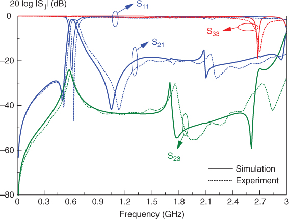
Next, the antenna part is studied. As can be seen from Fig. 2.28, the antenna has a resonance frequency of 2.7 GHz. The antenna bandwidth measured is about 1.7%, being higher than that for simulation (0.8%). The discrepancy can be caused by the omission of conductor and dielectric losses in the simulation. Figure 2.29 shows the electric current distribution on the conductor surface of the filter at 2.7 GHz, showing good isolation between the ports. The measured radiation patterns are shown in Fig. 2.30. As can be seen from the figure, the co-polarized fields are larger than their cross-polarized counterparts in both the E- and H-planes.
Figure 2.29 Electric current distribution on the antenna filter at resonance in Fig. 2.27. (Courtesy of Y. J. Sung, Kyonggi University. From (10), copyright © 2009 IEEE, with permission.)
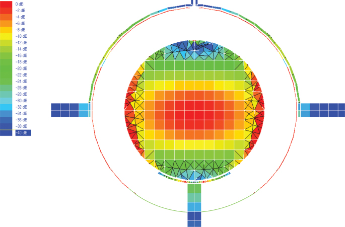
Figure 2.30 Measured normalized radiation patterns of the antenna part in Fig. 2.27. (Courtesy of Y. J. Sung, Kyonggi University. From (10), copyright © 2009 IEEE, with permission.)
2.2.3.3 Microstrip Ring–Slot Antenna Filter
Configuration
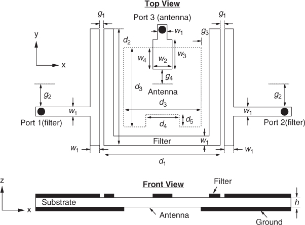
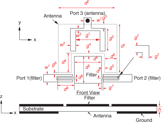
Figure 2.31 displays the configuration of the microstrip ring–slot antenna filter, where a wideband slot antenna (d3 = 35 mm, d4 = 10 mm, d5 = 5 mm, w1 = 1.99 mm, w2 = 10 mm, w3 = 17 mm, w4 = 16.5 mm, g3 = 0.51 mm, and g4 = 1 mm) is etched in the central part of a narrowband U-shaped microstrip filter (d1 = 40 mm, d2 = 35 mm, g1 = 0.2 mm, and g2 = 21.005 mm).
Figure 2.31 Antenna filter consisting of a slot antenna and a ring filter. (From (9), copyright © 2010 IEEE, with permission.)
Results and Discussion
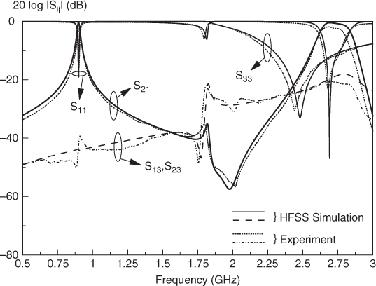
The simulated and measured reflection coefficients, insertion losses, and mutual couplings between different ports are shown in Fig. 2.32. First, the filter part is discussed. As can be seen from the figure, the measured and simulated resonance frequencies are 903.125 and 900.000 MHz (with an error of 0.35%), respectively. The measured and simulated insertion losses are 2.53 and 0.28 dB. It is observed that the measured 3-dB passband is about 20 MHz, which is slightly narrower than the simulated value of 22 MHz. The measured and simulated reflection coefficients (S11) at port 1 are 15.8 and 19.1 dB, respectively. It is worth mentioning that the higher-order mode of the filter (about 1.8 GHz) is suppressed well below 30 dB.
Figure 2.32 Simulated and measured reflection coefficients, insertion losses, and coupling coefficients of the antenna filter shown as a function of frequency. (From (9), © copyright 2010 IEEE, with permission.)
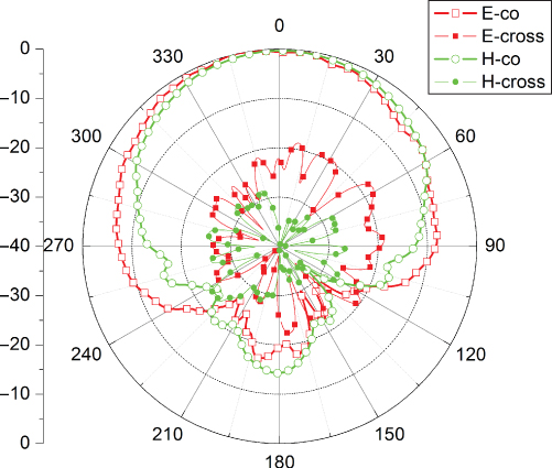
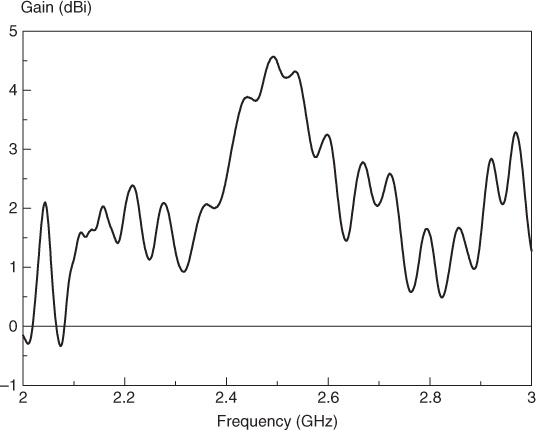
The antenna part of an antenna filter is investigated next. With reference to Fig. 2.32, the measured and simulated resonance frequencies at port 3 (S33) are given as 2.441 and 2.481 GHz (with an error of 1.7%), respectively. The measured and simulated impedance bandwidths (S33 ≤ − 10 dB) are 24 and 20.65%. A small resonance (∼1.75 GHz) is observed in the S33 curve, which should be due to the mutual coupling between the antenna and the filter. The measured and simulated radiation patterns of the antenna part are illustrated in Fig. 2.33 for both the E- and H-planes, showing reasonable agreement. As expected, the typical bidirectional patterns for the slot antenna (39) are obtained. Figure 2.34 shows the measured antenna gain, which is about 4.5 dBi at resonance.
Figure 2.33 Simulated and measured normalized radiation patterns of the antenna part of the antenna filter. (From (9), copyright © 2010 IEEE, with permission.)
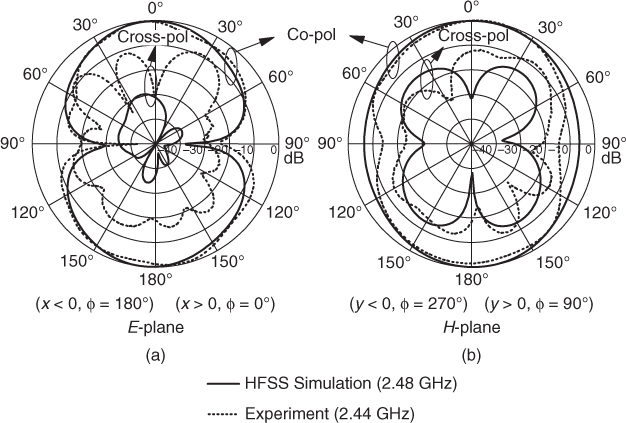
Figure 2.34 Measured antenna gain of the antenna filter. (From (9), copyright © 2010 IEEE, with permission.)
2.2.3.4 Ultrawideband Antenna Filter
In this section a three-port antenna filter that is made on a single substrate is proposed for ultrawideband (UWB) applications (11). It is constructed by closely integrating an UWB slot antenna with an UWB patch filter etched on the opposite side of the same substrate (Fig. 2.35). The coupling between the antenna and the filter is found to be very low, without needing any isolation layers.
Figure 2.35 Antenna filter constructed by integrating an ultrawideband slot antenna and a patch filter: (a) top view; (b) front view. (From (11), copyright © 2011 John Wiley & Sons, Inc., with permission.)
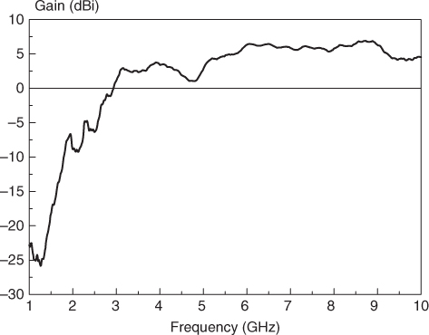
The filter part is studied first. Figure 2.36 shows the simulated and measured reflection coefficients and insertion losses of the filter part. It can be observed from the figure that the patch filter has three resonances. The measured 3-dB passband starts from 4 to 7.04 GHz, which agrees reasonably well with the simulated passband (3.93 to 7.1 GHz). The measured insertion loss (S21) is found to be less than 1.5 dB across the entire passband. Next, the antenna part of the IAF is investigated. The simulated and measured VSWRs of the U-shaped slot antenna are shown in Fig. 2.37. With reference to the figure, the simulated and measured passbands (VSWR < 2) at port 3 are 3.28 to 10 GHz and 3.17 to 10 GHz, respectively. Figure 2.38 shows the measured and simulated couplings (S13) between the antenna and filter ports. As can be seen from the figure, the coupling is generally weaker than 20 dB, even when g4 = g5 = 0 was used in the design. The results for S23 are similar but are not shown for brevity. Figure 2.39 shows the measured and simulated radiation patterns of the antenna part at 4 and 7 GHz, with reasonable agreement. With reference to the figure, the bidirectional radiations are quite stable as the frequency changes. For all of the cases, the cross-polarized fields are weaker than their co-polarized counterparts by about 20 dB in both the forward (θ = 0°) and backward (θ = 180°) directions. The measured antenna gain is shown in Fig. 2.40, where it is found that the gain varies between 1 and 7 dBi over the frequency range from 3 to 10 GHz.
Figure 2.36 Simulated and measured reflection coefficients and insertion losses of the filter part shown as a function of frequency. (From (11), copyright © 2011 John Wiley & Sons, Inc., with permission.)
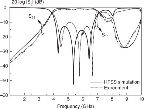
Figure 2.37 Simulated and measured VSWRs of the antenna part shown as a function of frequency. (From (11), copyright © 2011 John Wiley & Sons, Inc., with permission.)
Figure 2.38 Simulated and measured coupling coefficients between the antenna and filter parts of the antenna filter in Fig. 2.35. (From (11), copyright © 2011 John Wiley & Sons, Inc., with permission.)
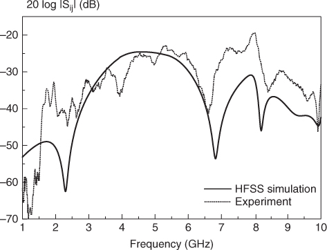
Figure 2.39 Simulated and measured normalized radiation patterns of the antenna part of the IAF in Fig. 2.35: (a) 4 GHz; (b) 7 GHz. (From (11), copyright © 2011 John Wiley & Sons, Inc., with permission.)
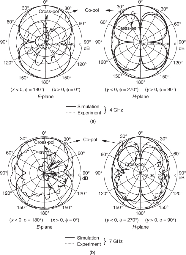
Figure 2.40 Measured antenna gain of the antenna part of the antenna filter in Fig. 2.35. (From (11), copyright © 2011 John Wiley & Sons, Inc., with permission.)
2.3 Balun Filters
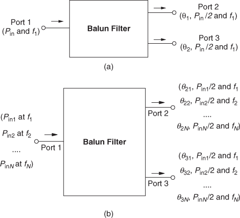
A balun (balanced-to-unbalanced) filter is a new component that combines the power dividing and filtering functions into one, with the single- and multiband configurations shown in Fig. 2.41(a) and 2.41(b), respectively. In each Nth of the passbands, a balun filter is designed to distribute an input power (PinN, N = 1, 2, … ) evenly to a pair of output ports, which have a phase difference of 180° (|θ2N − θ3N| = 180°). To be a dual function, each of the output ports itself must also be able to be made an independent filter. In recent years, research on the integration of balun and filter using different techniques has been reported (12–14, 40–44), . A ring resonator (12) and cross-slotted rectangular microstrip patch (40, 41) were used for exciting degenerate modes for a dual-mode balun filter. Dual-band cases are discussed in the literature (14, 43). The size of such a multifunctional component can be made very compact by using the LTCC technology (44). As neither the balun nor filter radiates, a balun filter can usually be modeled with reasonable accuracy by SPICE-based software.
Figure 2.41 Signal flows of a balun filter: (a) single-band; (b) multiband.
2.3.1 Ring Balun Filter
2.3.1.1 Configuration
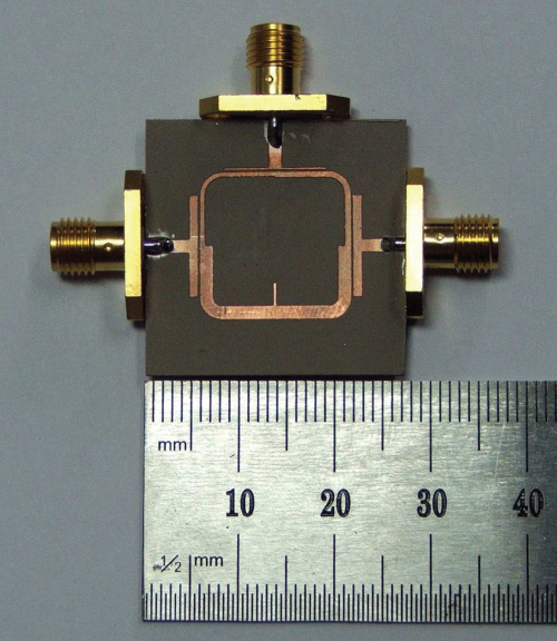
Jung and Hwang (12) first deployed a microstrip ring resonator as a dual-functional balun filter. It was made by cascading several sections of transmission lines, each of which has a different impedance, to form a dual-mode ring resonator. The ring has a one-wavelength circumference in total, with the configuration shown in Fig. 2.42. The design parameters are given by a = 0.60 mm, b = 0.75 mm, c = 1.46 mm, d = 0.30 mm, e = 0.90 mm, f = 0.36 mm, g = 2.40 mm, h = 0.10 mm, i = 16.14, and j = 17.90 mm (12). As can be seen from the figure, the resonator is capacitively coupled to an input and to the two outputs via narrow slits. For ease of analysis, it can be represented by a transmission-line model, as shown in Fig. 2.43. With reference to the figure, the ring can be equally divided into four portions, having characteristic impedances of Z1, Z2, Z3, and Z4. Figure 2.44 shows a prototype balun filter.
Figure 2.42 Top-down view of a microstrip ring balun filter. (Courtesy of H.-Y. Hwang, Kangwon National University. From (12). copyright © 2007 IEEE, with permission.)
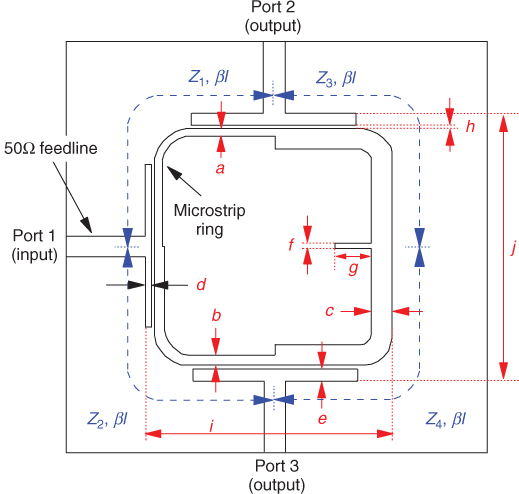
Figure 2.43 Equivalent circuit for the microstrip balun filter in Fig. 2.42. (Courtesy of H.-Y. Hwang, Kangwon National University. From (12). copyright © 2007 IEEE, with permission.)
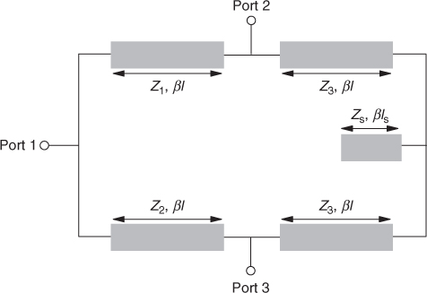
Figure 2.44 Balun filter. (Courtesy of H.-Y. Hwang, Kangwon National University. From (12), copyright © 2007 IEEE, with permission.)
2.3.1.2 Results and Discussion
Given in Fig. 2.45 are the simulated S parameters generated by the circuit simulator ADS. Also sketched on the same figure are the results measured. It is observed that the measurement agrees very well with the transmission-line model, given in Fig. 2.43. As can be seen from Fig. 2.45, each of the two output ports has a bandpassing 3-dB bandwidth [![]() ] of about 1.6%, operating in the frequency range 2.425 to 2.465 GHz. The center frequency is given by f0 ∼ 2.44 GHz.
] of about 1.6%, operating in the frequency range 2.425 to 2.465 GHz. The center frequency is given by f0 ∼ 2.44 GHz. ![]() and
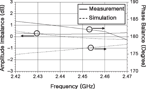
and ![]() are the frequencies at which the signal power reduces by half at the upper and lower bounds of the passband, respectively. The insertion loss is about 5.5 dB, as can be seen from Fig. 2.45. Next, the amplitude and phase imbalances of the balun are measured. With reference to Fig. 2.46, the amplitude imbalance and phase difference between the two balanced ports are well within 0.5 dB and 180 ± 5°, respectively, in the passband.
are the frequencies at which the signal power reduces by half at the upper and lower bounds of the passband, respectively. The insertion loss is about 5.5 dB, as can be seen from Fig. 2.45. Next, the amplitude and phase imbalances of the balun are measured. With reference to Fig. 2.46, the amplitude imbalance and phase difference between the two balanced ports are well within 0.5 dB and 180 ± 5°, respectively, in the passband.
Figure 2.45 Simulated and measured S parameters of the microstrip balun filter in Fig. 2.42. (Courtesy of H.-Y. Hwang, Kangwon National University. From (12), copyright © 2007 IEEE, with permission.)
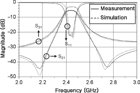
Figure 2.46 Simulated and measured amplitude and phase imbalances of the microstrip balun filter in Fig. 2.42. (Courtesy of H.-Y. Hwang, Kangwon National University. From (12), copyright © 2007 IEEE, with permission.)
2.3.2 Magnetic-Coupled Balun Filter
2.3.2.1 Configuration
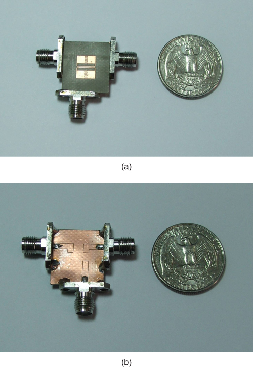
Figure 2.47 shows a balun filter that is designed using a pair of magnetically coupled resonators (13). As can be seen from the figure, interdigital configuration was used to minimize the circuit size. The design parameters are ls = 1.2 mm, wc = 2.5 mm, lc = 1.3 mm, gc = 0.1 mm, fw = 0.2 mm, and ce = 1.7 mm. It can be represented by the equivalent-circuit model shown in Fig. 2.48, where the component parameters are given by C = 0.24 pF, L = 2.45 nH, Ls = 1.2 nH, Cg = 0.06 pF, Cp = 0.72 pF, ![]() pF, Ce = 0.21 pF, and M = 0.08. The prototype is shown in Fig. 2.49.
pF, Ce = 0.21 pF, and M = 0.08. The prototype is shown in Fig. 2.49.
Figure 2.47 Top-down view of a CPW magnetic-coupled balun filter. (Courtesy of J. Lee, Chonnam National University. From (13), copyright © 2009 IEEE, with permission.)
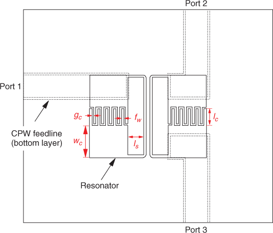
Figure 2.48 Equivalent-circuit model of the CPW magnetic-coupled balun filter in Fig. 2.47. (Courtesy of J. Lee, Chonnam National University. From (13), copyright © 2009 IEEE, with permission.)
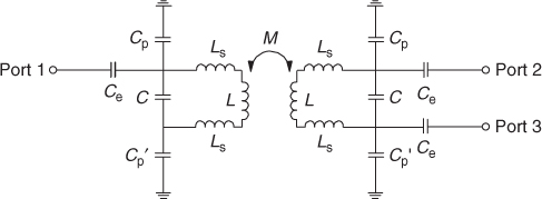
Figure 2.49 CPW magnetic-coupled balun filter: (a) top view; (b) back view. (Courtesy of J. Lee, Chonnam National University. From (13), copyright © 2009 IEEE, with permission.)
2.3.2.2 Results and Discussion
In Fig. 2.50 an equivalent-circuit model was used to generate the simulation results, then verified with experiments. As can be seen from the figure, the measured reflection coefficient and insertion loss at the unbalanced port are below −15 and −5.5 dB, respectively, in the passband from 2.4 to 2.5 GHz. With reference to Fig. 2.51, the phase difference measured is within 180 ± 2°, and the measured amplitude imbalance is well below 2 dB.
Figure 2.50 Measured and modeled S parameters of a magnetic-coupled balun filter in Fig. 2.47. (Courtesy of J. Lee, Chonnam National University. From (13), copyright © 2009 IEEE, with permission.)
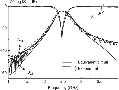
Figure 2.51 Measured phase difference and amplitude imbalance of the magnetic-coupled balun filter in Fig. 2.47. (Courtesy of J. Lee, Chonnam National University. From (13), copyright © 2009 IEEE, with permission.)
2.3.3 Rectangular Patch Balun Filter
2.3.3.1 Configuration
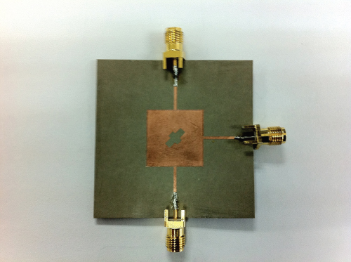
In (45, 46), unequal crossed slots were etched on a microstrip rectangular patch for producing double modes in a bandpass filter. This perturbation method is similar to that used by a CP antenna in which two degenerate modes are excited by introducing disturbance to the resonator geometry. The unloaded Q factor of such a filter is usually in the range 100 to 300. With the use of the same technique, a patch balun filter (40) was designed and is shown in Fig. 2.52. As can be seen from the figure, cross-slots are again used for generating two degenerate modes in a rectangular patch. It works as two independent dual-mode filters in the signal paths of port 1–2 and port 1–3. At the same time, it is a good balun that divides a microwave signal evenly into two with 180° phase difference between them. Long capacitive gaps are placed along the patch edges to effectively couple microwave signals to ports 2 and 3. Other design parameters are given by W = 18 mm , w1 = 0.933 mm, w2 = 0.2 mm, g1 = 0.2 mm g2 = 0.1335 mm, g3 = 0.1 mm, g4 = 0.07 mm. l1 = 7 mm, l2 = 4 mm, d = 2 mm, and ϕ′ = 45°. It is made on a grounded substrate (50 × 50 mm2) with a dielectric constant of ε r = 6.15 and a thickness of 0.635 mm. The prototype is shown in Fig. 2.53.
Figure 2.52 Top-down view of a microstrip patch balun filter, with crossed slots. (Courtesy of C. H. Ng, Agilent Technologies Sdn. Bhd., Malaysia. From (40).)
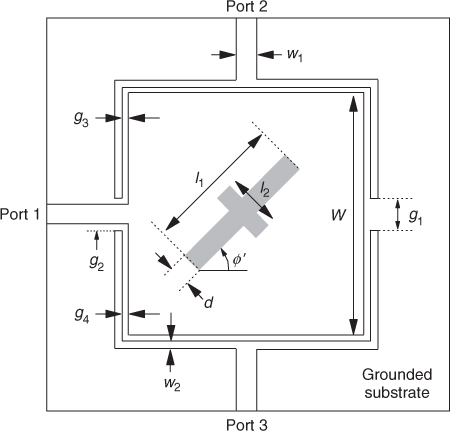
Figure 2.53 Microstrip patch balun filter. (Courtesy of C. H. Ng, Agilent Technologies Sdn. Bhd., Malaysia. From (40).)
2.3.3.2 Results and Discussion
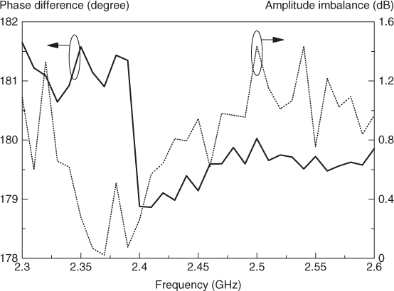
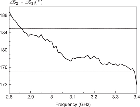
Ansoft HFSS was used to simulate a microstrip patch balun filter, and the results were later verified with experiments. Figure 2.54 shows the simulated and measured S parameters as a function of frequency. In general, reasonable agreement is found between simulation and measurement. For both S21 and S31, the measured 3-dB filter passband covers 2.91 to 3.19 GHz, centering at 3.05 GHz. Two transmission zeros are also observed in S31 near the filter passband. With reference to the same figure, the output signal magnitudes (|S21| and |S31|) are equal at about −6 dB. Additional losses can be introduced by the connectors and feedlines. Figure 2.55 gives the measured output phase of the microstrip patch balun filter. As can be seen from the figure, the phase bandwidth (180 ± 5°) encompasses 2.86 to almost 3.4 GHz.
Figure 2.54 Simulated and measured S parameters of the microstrip patch balun filter in Fig. 2.52. (Courtesy of C. H. Ng, Agilent Technologies Sdn. Bhd., Malaysia. From (40).)
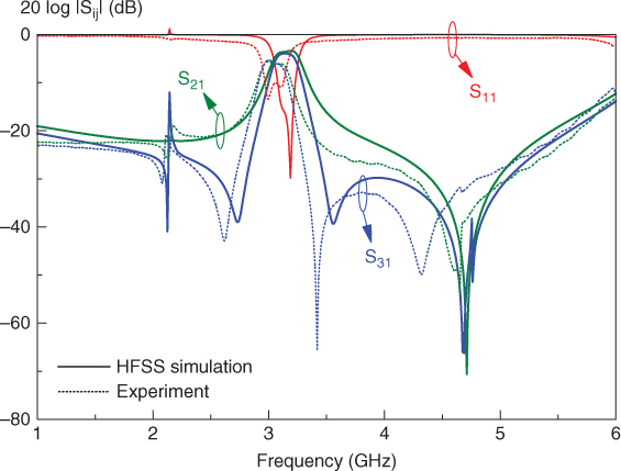
Figure 2.55 Measured output phase of the microstrip patch balun filter in Fig. 2.52. (Courtesy of C. H. Ng, Agilent Technologies Sdn. Bhd., Malaysia. From (40).)
2.4 Antenna Package
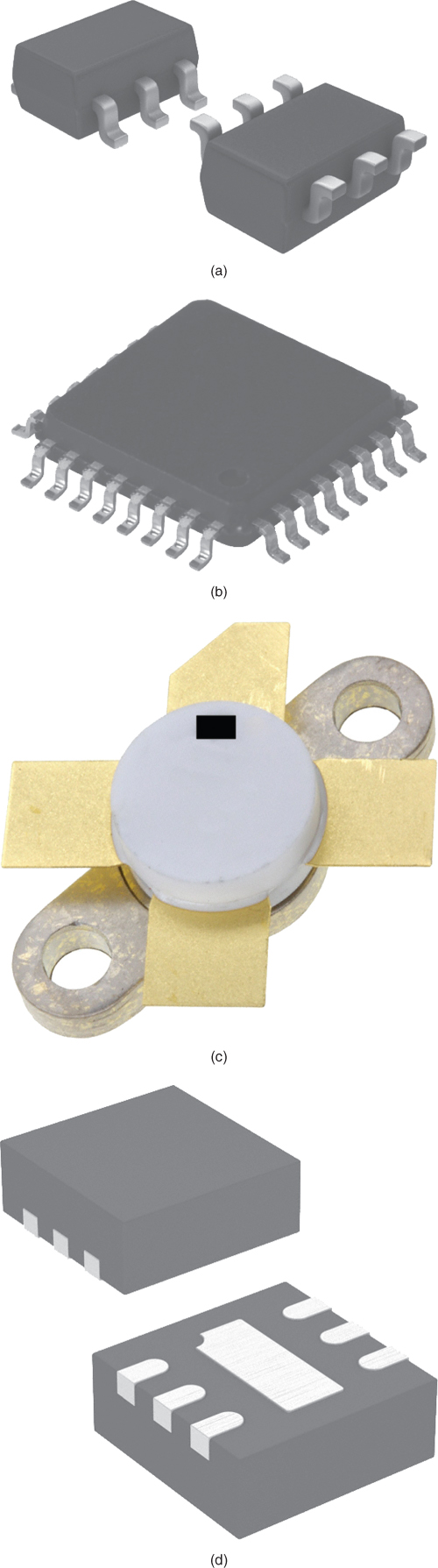
Packaging cover is required by most electronic devices for electrical connection with other circuits, protection from mechanical damage and dirt, dissipation of excess heat generated by the circuit, and shielding from electromagnetic interference and electrostatic discharge (16). In modern electronic systems, packages are also designed into different shapes for aesthetics and marketing considerations. As the chemical materials that made the integrated circuits can be harmful to the environment, a package is also required to enhance the product safety and preventing contamination. Figure 2.56 shows some of the contemporary packages for microwave circuits in the commercial market. As the package is much bulkier than a semiconductor chip, there is a strong desire to limit its footprint and size. Recently, some works were conducted to explore using the packaging cover as the radiating element (16, 17).
Figure 2.56 Contemporary microwave packages: (a) small outline package (SOP); (b) quad flat package (QFP); (c) transistor outline (TO) package; (d) dual-flat no-leads (DFN) package.
2.4.1 DRA Packaging Cover
2.4.1.1 Configuration
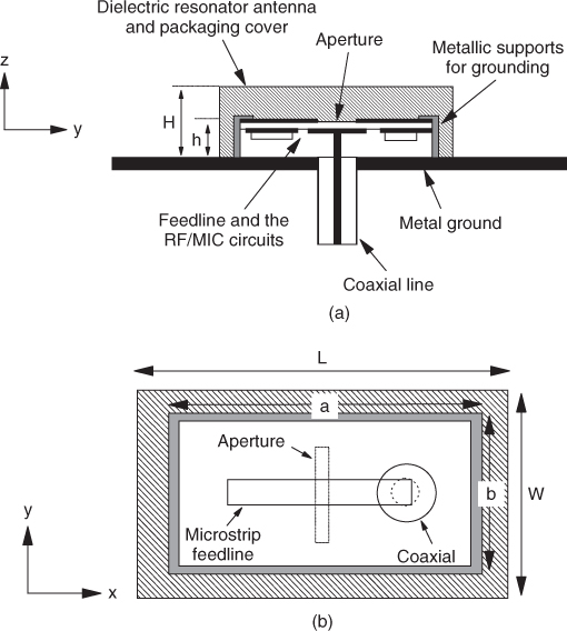
The use of a DRA as a packaging cover was first explored by Lim and Leung (16). Two configurations were proposed, with the first shown in Fig. 2.57. Being a packaging cover simultaneously, a rectangular hollow DRA (with dimensions L = 30 mm, W = 29 mm, and H = 15 mm) is excited by a microstrip-fed aperture etched on the top of a concentric rectangular metallic cavity (with dimensions a = 15 mm, b = 21.6 mm, and h = 5 mm). In the experiment, a microstrip feedline is connected to the center conductor of an external coaxial line for excitation of the DRA. In practice, however, the feedline can be connected to either active or passive devices that are shielded inside the cavity. The packaging DRA operating at 2.4 GHz can be designed using the following procedure:
Figure 2.57 Rectangular hollow DRA excited by a microstrip-fed aperture: (a) side view; (b) top view. (From (16), copyright © 2006 IEEE, with permission.)
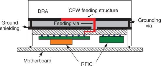
The aforementioned three-step procedure can be used to design and tune the operating frequency of the DRA. The Eccostock HiK Powder (49), a kind of fine-granular and free-flowing powder with dielectric constant of ε r = 12 was used as the dielectric material. It was noted that slight jogging is generally sufficient to obtain even powder density in the container, and no further postprocessing is required. The dielectric properties of the HiK powder were well tested as described by Junker et al. (50). In the experiment, a few hard-form clad boards ( ε r ∼ 1) were used to construct a rectangular container for the powder. With reference to Fig. 2.57, the faces of the rectangular metallic cavity are formed by a Duroid substrate (top face, with a thickness of 0.762 mm) and four metallic supports (sidewalls), concentrically in the air region of the hollow DRA. A microstrip-fed aperture is etched in the ground plane of the microstrip for exciting the DRA. The aperture has a length of 0.2063λe, where ![]() . The ground plane of the microstrip also acts as the electrical ground for the RF/MIC circuits located on the opposite side of the substrate, as can be seen in Fig. 2.58. The substrate grounding is connected to the main electrical ground plane through the metallic supports. To demonstrate the design idea, an amplifier is used as the active device.
. The ground plane of the microstrip also acts as the electrical ground for the RF/MIC circuits located on the opposite side of the substrate, as can be seen in Fig. 2.58. The substrate grounding is connected to the main electrical ground plane through the metallic supports. To demonstrate the design idea, an amplifier is used as the active device.
Figure 2.58 Rectangular hollow DRA with an airgap, excited by a microstrip-fed aperture: (a) side view; (b) top view. (From (16), copyright © 2006 IEEE, with permission.)
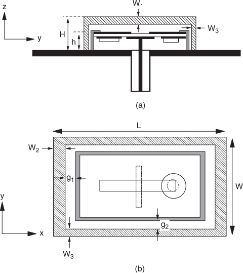
The second configuration is shown in Fig. 2.58, where the metallic cavity and circuits are inserted into the hollow region of the DRA, which has dimensions of L = 12.7 mm, W = 9 mm, H = 6.35 mm, h = 3 mm, W1 = 1.85 mm, W2 = 1.85 mm, W3 = 1.3 mm, g1 = 0.055 mm, and g2 = 0.025 mm. In this case, simulation results show that field coupling can be efficient only when the dielectric constant is sufficiently high. Here, the dielectric constant is chosen to be ε r = 82. The DRA packaging cover in Fig. 2.58 provides more manufacturing ease, as the dielectric resonator is easily removable. The aforementioned design procedure is applicable to this DRA.
2.4.1.2 Results and Discussion
In Fig. 2.59 the simulated and measured reflection coefficients are shown as a function of frequency for the antenna in Fig. 2.57. The measured impedance bandwidth (S11 ≤ − 10 dB) is 5.6%, slightly higher than for the simulation (4%). Good agreement is found between the measured (2.42 GHz) and simulated (2.40 GHz) resonance frequencies. The input impedance is shown in the inset of Fig. 2.59. In Fig. 2.60, the simulated and measured normalized radiation patterns are shown for both the E- (xz-plane) and H-plane (yz-plane) at 2.42 GHz, where the broadside TE mode is obtained as expected. The co-polarized fields are in general 20 dB stronger than their cross-polarized counterparts in the boresight direction (θ = 0°).
Figure 2.59 Simulated and measured reflection coefficients of the hollow DRA with an embedded metallic cavity (Fig. 2.57). The inset shows the simulated and measured input impedances of the hollow DRA as a function of frequency. (From (16), copyright © 2006 IEEE, with permission.)
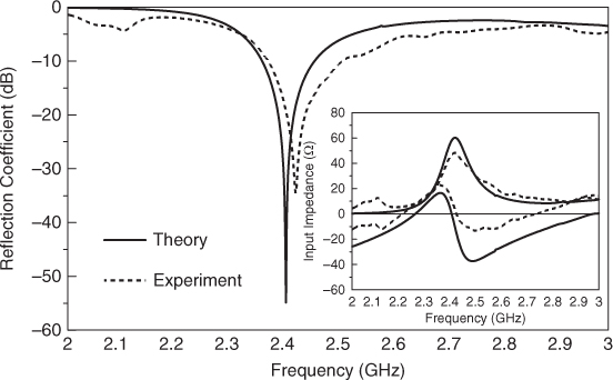
Figure 2.60 Simulated and measured normalized radiation patterns of a rectangular hollow DRA in Fig. 2.57: (a) E-plane (xz-plane); (b) H-plane (yz-plane). (From (16), copyright © 2006 IEEE, with permission.)
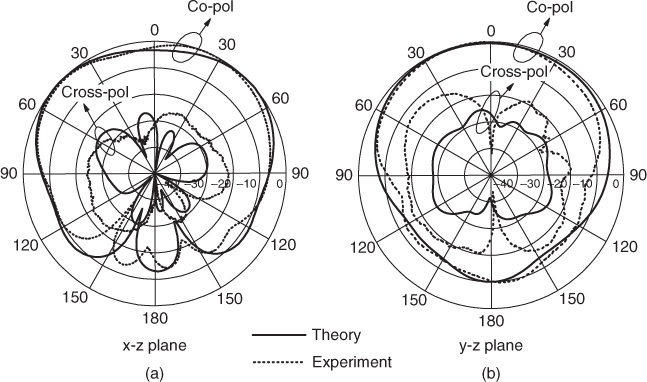
Figure 2.61 shows the simulated reflection coefficient and normalized radiation patterns for the DRA configuration in Fig. 2.58. The input impedance is also given in the inset of Fig. 2.61(a). With reference to the figure, the simulated impedance bandwidth is about 1.2% at the fundamental resonance frequency of 3.43 GHz. It is reasonable for a high-permittivity DRA. The radiation patterns are broad-side, with the co-polarized fields larger than the cross-polarized ones by at least 20 dB in the bore-sight direction. To further study the integration of the DRA packaging cover with active devices. An Agilent AG302-86 low-noise amplifier (LNA), which has a typical gain of 13.6 dB at 2.4 GHz, was selected to integrate with the DRA shown in Fig. 2.57, whose schematic diagram is shown in the inset of Fig. 2.62. This commercial LNA is prematched to 50 Ω at the input. It is connected to the microstrip feed of the antenna. In an experiment, a small through-hole was drilled on the main ground plane to supply dc bias to the LNA. By combining the DRA and the LNA, an active DRA is designed for transceiver front ends. At the output of the LNA, when it is functioning as a receiver with the dc supply turned on, the measured reflection coefficient of the active DRA is shown in Fig. 2.62. It is noted that the parasitics of the amplifier have shifted the fundamental resonance frequency to around 2.5 GHz, slightly higher than that for the passive DRA. With reference to the figure, two dips are observed at 2.58 and 2.66 GHz, which can be caused by the matching circuits. To investigate the effect of the amplifier on the transmitting characteristics, the active DRA is reconfigured as a transmitter using the same amplifier, and the measured reflection coefficient is also shown in Fig. 2.62. Again, the resonance frequency has drifted to about 2.5 GHz.
Figure 2.61 Simulated (a) reflection coefficient and (b) normalized radiation patterns of the rectangular hollow DRA, with an airgap around the embedded metallic cavity (Fig. 2.58). The inset in part (a) shows the simulated input impedance as a function of frequency. (From (16), copyright © 2006 IEEE, with permission.)
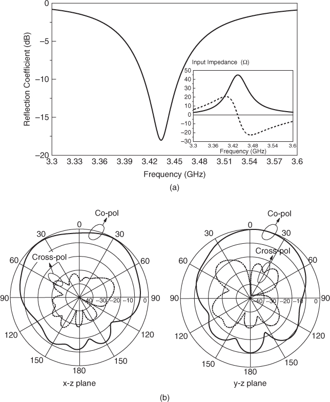
Figure 2.62 Comparison of the measured reflection coefficients of the passive and active DRAs (as receiver or transmitter) in Fig. 2.57. (From (16), copyright © 2006 IEEE, with permission.)
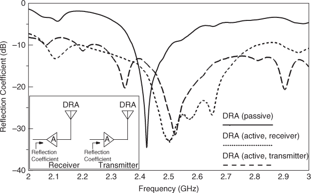
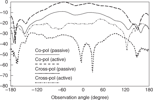
Figure 2.63 shows the measured co-polarized radiation pattern of the active DRA (in receiver mode) in the E-plane (the xz-plane) at 2.42 GHz. An amplifier gain ranging from 7 to 12 dB is observed across the observation angle for the active DRA. The cross-polarized fields of both the passive and active DRAs are also plotted in Fig. 2.63. For ease of comparison, all of the radiation patterns are normalized to the maximum value of the co-polarized field of the active DRA. The gain loss (as compared to specification data) can be caused by unavoidable impedance variations and imperfections in the experiment.
Figure 2.63 Comparison of measured E-plane co-polarized and cross-polarized fields between the passive and active DRAs in Fig. 2.57. (From (16), copyright © 2006 IEEE, with permission.)
2.4.2 Other Antenna Packages
In Fig. 2.64 a cylindrical DRA was stacked on top of a shielded package for use as a USB dongle. The DRA was excited by a meandered magnetic loop, being fed by a co-planar waveguide. Other microwave components and devices are all encapsulated inside a shielded metallic cavity. Here, the DR is used simultaneously as a radiating element and a protective layer for the underlying cavity. As the DRA occupies virtually no extra space, the dongle can achieve a very compact size. Such a top-loading DRA can easily be made on a chip to operate at millimeter-wave frequencies by employing the semiconductor fabrication technology (51).
Figure 2.64 Side view of a wireless module proposed by Rotaru et al. (17) using the package integrated antenna approach.
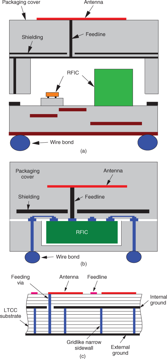
Recently, antenna-on-package (AOP) (52, 53), antenna-in-package (AiP) (54), and low-temperature co-fired ceramics (LTCC) (55) techniques have been applied to integrate an antenna with various semiconductor chips and packages. The typical configurations are shown in Fig. 2.65. As can be seen from Fig. 2.65(a), the AOP technology stacks an antenna directly on top of a packaging cover using the system-on-package (SOP) technology (37, 53). On the other hand, an antenna is usually embedded inside the package for the AiP (54), as can be seen from Fig. 2.65(b). With the recent developments in material science, the LTCC technique has become a popular way for fabricating microwave- and millimeter-wave systems (55, 56). The main advantage is that densely packed passive circuits can be squeezed into multiple layers of stacked dielectrics. An example of an LTCC millimeter-wave system that is made of 12 dielectric layers is shown in Fig. 2.65(c).
Figure 2.65 Configurations of various integrated antennas: (a) AOP (from (52)); (b) AiP (from (54)); (c) LTCC (from (55)).
2.5 Conclusions
In this chapter, several multifunction microwave modules, such as an antenna filter, a balun filter, and an antenna packaging cover, have been discussed. The art and science of PICs is still in a state of rapid development. Market demand for a more compact and less expensive multifunction component is constantly on the rise. As metal is lossy in the millimeter-wave range, the trend is towards merging several functions into a single module for a shorter signal transmission path. Better signal integrity is usually achievable by having a smaller component number and shortening the connection wires on a circuit board. It is foreseeable that in the near future more and more multifunction microwave- and millimeter-wave devices will be explored and studied.
References
1. J. Lin and T. Itoh, Active integrated antennas, IEEE Trans. Microwave Theory Tech., vol. 42, pp. 2186–2194, Dec. 1994.
2. Y. Qian and T. Itoh, Progress in active integrated antennas and their applications, IEEE Trans. Microwave Theory Tech., vol. 46, pp. 1891–1900, Nov. 1998.
3. K. Chang, R. A. York, P. S. Hall, and T. Itoh, Active integrated antennas, IEEE Trans. Microwave Theory Tech., vol. 50, pp. 937–944, Mar. 2002.
4. K. C. Gupta and P. S. Hall, Analysis and Design of Integrated Circuit Antenna Modules. New York: Wiley, 2000.
5. J. A. Navarro and K. Chang, Integrated Active Antennas and Spatial Power Combining. New York: Wiley, 1996.
6. E. H. Lim and K. W. Leung, Use of the dielectric resonator antenna as a filter element, IEEE Trans. Antennas Propag., vol. 56, pp. 5–10, Jan. 2008.
7. L. K. Hady, D. Kajfez, and A. A. Kishk, Triple mode use of a single dielectric resonator, IEEE Trans. Antennas Propag., vol. 57, pp. 1328–1335, May 2009.
8. L. K. Hady, D. Kajfez, and A. A. Kishk, Dielectric resonator antenna in a polarization filtering cavity for dual function applications, IEEE Trans. Microwave Theory Tech., vol. 56, pp. 3079–3085, Dec. 2008.
9. E. H. Lim and K. W. Leung, Compact three-port integrated-antenna–filter modules, IEEE Antennas Wireless Propag. Lett., vol. 9, pp. 467–470, May 2010.
10. Y. J. Sung, Microstrip resonator doubling as a filter and as an antenna, IEEE Antennas Wireless Propag. Lett., vol. 8, pp. 486–489, Mar. 2009.
11. E. H. Lim and K. W. Leung, Ultrawideband microstrip integrated-antenna–filter, Microwave Opt. Tech. Lett., vol. 53, no. 1, pp. 32–34, Jan. 2011.
12. E. Jung and H. Hwang, A balun-BPF using a dual mode ring resonator, IEEE Microwave Wireless Compor. Lett., vol. 17, pp. 652–654, Sept. 2007.
13. J. Lee, H. Lee, H. Nam, and Y. Lim, “Balun-BPF using magnetically coupled interdigital-loop resonators,” 6th International Conference on Electrical Engineering/Electronics, Computer, Telecommunications and Information Technology, 2009, Pattaya, May 2009, pp. 932–935.
14. L. K. Yeung and K. L. Wu, A dual-band coupled-line balun filter, IEEE Trans. Microwave Theory Tech., vol. 55, pp. 2406–2411, Nov. 2007.
15. Z. Zuo, X. Chen, G. Han, L. Li, and W. Zhang, An integrated approach to RF antenna–filter co-design, IEEE Antennas Wireless Propag. Lett., vol. 8, pp. 141–144, Apr. 2009.
16. E. H. Lim and K. W. Leung, Novel application of the hollow dielectric antenna as a packaging cover, IEEE Trans. Antennas Propag., vol. 54, pp. 484–487, Feb. 2006.
17. M. Rotaru, Y. Y. Lim, H. Kuruveettil, R. Yang, A. P. Popov, and C. Chua, Implementation of packaged integrated antenna with embedded front end for Bluetooth applications, IEEE Trans. Adv. Packag., vol. 31, no. 3, pp. 558–567, Aug. 2008.
18. R. S. Adams, B. O. Neil, and J. F. Young, The circulator and antenna as a single integrated system, IEEE Antennas Wireless Propag. Lett., vol. 8, pp. 165–168, May 2008.
19. W. Lim, W. Son, K. S. Oh, W. Kim, and J. Yu, Compact integrated antenna with circulator for UHF RFID system, IEEE Antennas Wireless Propag. Lett., vol. 7, pp. 673–675, Mar. 2008.
20. S. B. Cohn, Microwave bandpass filters containing high-Q dielectric resonators, IEEE Trans. Microwave Theory Tech., vol. 16, pp. 218–227, Apr. 1968.
21. H. Abe, Y. Takayama, A. Higashisaka, and H. Takamizawa, A highly stabilized low-noise GaAs FET integrated oscillator with a dielectric resonator in the C band, IEEE Trans. Microwave Theory Tech., vol. 26, pp. 156–162, Mar. 1978.
22. S. A. Long, M. W. McAllister, and L. C. Shen, The resonant cylindrical dielectric cavity antenna, IEEE Trans. Antennas Propag., vol. 31, pp. 406–412, May 1983.
23. K. M. Luk and K. W. Leung, Eds., Dielectric Resonator Antennas. Hertfordshire, UK: Research Studies Press, 2003.
24. A. Petosa, Dielectric Resonator Antenna Handbook. Norwood, MA: Artech House, 2007.
25. D. Kajfez and P. Guillon, Dielectric Resonators. Atlanta, GA: Noble, 1998.
26. T. D. Iveland, Dielectric resonator filters for application in microwave integrated circuits, IEEE Trans. Microwave Theory Tech., vol. 19, pp. 643–652, July 1971.
27. C. Wang, K. A. Zaki, A. E. Atia, and T. G. Dolan, Dielectric combline resonators and filters, IEEE Trans. Microwave Theory Tech., vol. 46, pp. 2501–2506, Dec. 1998.
28. S. J. Fiedziuszko and S. Holme, Dielectric resonators raising your high-Q, IEEE Microwave Mag., Sept. 2001.
29. I. J. Bahl and P. Bhartia, Microstrip Antennas. Norwood, MA: Artech House, 1980.
30. J. S. Hong and M. J. Lancaster, Microstrip Filters for RF/Microwave Applications. New York: Wiley, 2001.
31. L. H. Hsieh and K. Chang, Equivalent lumped elements G, L, C, and unloaded Q's of closed- and open-loop ring resonators, IEEE Trans. Microwave Theory Tech., vol. 50, pp. 453–460, Feb. 2002.
32. R. R. Mansour, Filter technologies for wireless base stations, IEEE Antennas Propag. Mag., vol. 5, no. 1, pp. 68–74, Mar. 2004.
33. E. Pistono, P. Ferrari, L. Duvillaret, J. Duchamp, and R. G. Harrison, Hybrid narrow-band tunable bandpass filter based on varactor loaded electromagnetic-bandgap coplanar waveguides, IEEE Trans. Microwave Theory Tech., vol. 53, pp. 2506–2514, Aug. 2005.
34. S. K. Vaibhav, V. V. Mishra, and A. Biswas, A modified ring dielectric resonator with improved mode separation and its tunability characteristics in MIC environment, IEEE Trans. Microwave Theory Tech., vol. 53, pp. 1960–1967, June 2005.
35. Y. P. Zhang, X. J. Li, and T. Y. Phang, A study of dual-mode bandpass filter integrated in BGA package for single-chip RF transceivers, IEEE Trans. Adv. Packag., vol. 29, no. 2, pp. 354–358, May 2006.
36. L. K. Yeung and K. L. Wu, An LTCC balanced-to-unbalanced extracted-pole bandpass filter with complex load, IEEE Trans. Microwave Theory Tech., vol. 54, pp. 1512–1518, Apr. 2006.
37. Y. P. Zhang, Integrated circuit ceramic ball grid array package antenna, IEEE Trans. Antennas Propag., vol. 52, pp. 2538–2544, Oct. 2004.
38. K. Chang and L. H. Hsieh, Microwave Ring Circuits and Related Structures. Hoboken, NJ: Wiley, 2004.
39. R. Garg, P. Bhartia, I. Bahl, and A. Ittipiboon, Microstrip Antenna Design Handbook. Dedham, MA: Artech House, 2001.
40. C. H. Ng, E. H. Lim, and K. W. Leung, “Microstrip patch balun filter,” Cross Strait Quad-Regional Radio Science and Wireless Technology Conference, Harbin, China, July 28, 2011.
41. S. Sun and W. Menzel, Novel dual-mode balun bandpass filters using single cross-slotted patch resonator, IEEE Microwave Wireless Compon. Lett., vol. 21, pp. 415–417, Aug. 2011.
42. C. H. Hu, C. H. Wang, S. Y. Chen, and C. H. Chen, Balanced-to-unbalanced bandpass filters and the antenna application, IEEE Trans. Microwave Theory Tech., vol. 56, pp. 2474–2482, Nov. 2008.
43. G. S. Huang and C. H. Chen, Dual-band balun bandpass filter with hybrid structure, IEEE Microwave Wireless Compon. Lett., vol. 21, pp. 356–358, July 2011.
44. G. H. Huang, C. H. Hu, and C. H. Chen, LTCC balun bandpass filters using dual-response resonators, IEEE Microwave Wireless Compon. Lett., vol. 21, pp. 483–485, Sept. 2011.
45. L. Zhu, P. M. Wecowski, and K. Wu, New planar dual-mode filter using cross-slotted patch resonator for simultaneous size and loss reduction, IEEE Trans. Microwave Theory Tech., vol. 47, no. 5, pp. 650–654, May 1999.
46. L. H. Hsieh and K. Chang, Compact size and low insertion loss Chebyshev-function bandpass filters using dual-mode patch resonators, Electron. Lett., vol. 37, no. 17, Aug. 2001.
47. R. K. Mongia and A. Ittipiboon, Theoretical and experimental investigations on rectangular dielectric resonator antennas, IEEE Trans. Antennas Propag., vol. 45, pp. 1348–1356, Sept. 1997.
48. A. Petosa, A. Ittipiboon, Y. M. M. Antar, D. Roscoe, and M. Cuhaci, Recent advances in dielectric-resonator antenna technology, IEEE Antennas Propag. Mag., vol. 40, pp. 35–48, June 1998.
49. Product Manual for Eccostock HiK Powder, Emerson & Cuming Microwave Product. http://www.eccosorb.com/catalog/eccostock/HIKPOWDER.pdf.
50. G. P. Junker, A. A. Kishk, and A. W. Glisson, Input impedance of dielectric resonator antennas excited by a coaxial probe, IEEE Trans. Antennas Propag., vol. 42, pp. 960–966, July 1994.
51. M. Nezhad-Ahmadi, M. Fakharzadeh, B. Biglarbegian, and S. Safavi-Naeini, Input impedance of dielectric resonator antennas excited by a coaxial high-efficiency on-chip dielectric resonator antenna for mm-wave transceivers, IEEE Trans. Antennas Propag., vol. 58, pp. 3388–3392, Oct. 2010.
52. S. Brebels, J. Ryckaert, B. Come, S. Donnay, W. D. Raedt, E. Beyne, and R. P. Mertens, SOP integration and codesign of antennas, IEEE Trans. Adv. Packag., vol. 27, no. 2, pp. 341–351, May 2004.
53. M. M. Tentzeris, J. Laskar, J. Papapolymerou, S. Pinel, V. Palazzari, G. DeJean, N. Papageorgiou, J. Thompson, R. Bairavasubramanian, S. Sarkar, and J. H. Lee, 3-D-integrated RF and millimeter-wave functions and modules using liquid crystal polymer (LCP) system-on-package technology, IEEE Trans. Adv. Packag., vol. 27, no. 2, pp. 332–340, May 2004.
54. Y. P. Zhang, Antenna-on-chip and antenna-in-package solutions to highly integrated millimeter-wave devices for wireless communications, IEEE Trans. Antennas Propag., vol. 52, pp. 2538–2544, Oct. 2004.
55. Y. Huang, K. L. Wu, D. G. Fang, and M. Ehlert, An integrated LTCC millimeter-wave planar array antenna with low-loss feeding network, IEEE Trans. Antennas Propag., vol. 53, pp. 1232–1234, Mar. 2005.
56. Y. Q. Zhang, Y. X. Guo, and M. S. Leong, A novel multilayer UWB antenna on LTCC, IEEE Trans. Antennas Propag., vol. 58, pp. 3013–3019, Sept. 2010.