
Chapter 1
Compact Multifunctional Antennas in Microwave Wireless Systems
1.1 Introduction
The mission of a communication system is to get messages delivered with minimum distortion. Messages such as voices, pictures, and movies are a series of natural signals over time, operating at frequencies ranging from a few to hundreds of kilohertz. Figure 1.1 shows the signal flows in a communication system. There are two types of communication systems: wired and wireless. Examples of wired systems are telephony and optical systems in which cables and fibers are deployed for transmitting signals, respectively. The telephone, patented by Alexander Graham Bell in 1876 (1), was the earliest available communication gadget that enabled the conversion of vocal messages into electronic signals. In 1966, Charles Kao (2) showed that a glass strand is able to be made into a signal-transmitting medium. Since then, tens of thousands of miles of optical fibers have been laid to carry information on land and across the oceans. The rapid advancement of optical technologies makes possible the transmission of signals in bulk using light, and it has led to a surge of internet technologies since the last century. However, the major drawback of wired communications is that it does not allow user mobility. Geographical features and human-made constructions can also pose a hindrance for laying out long wires or cables. As early as 1900, it was shown by Guglielmo Marconi that an electromagnetic wave is able to carry signals through air and free space. Since then, numerous analog and digital wireless communication systems have been developed. Figure 1.2 shows a typical analog wireless system, which has many functional blocks performing complex operations such as reception, transmission, modulation, and demodulation. As can be seen from the figure, the transmitting path consists basically of a modulator and a radio-frequency (RF) transmitter, while the receiving path has a demodulator and an RF receiver. In an analog wireless system all the signals are continuous. As shown in Fig. 1.3, the system can easily be made digital by incorporating analog-to-digital and digital-to-analog converters. In modern digital wireless systems, the modulation, demodulation, coding, and decoding processes can be performed easily by superfast microprocessors and digital signal processors. An advantage of digital signal is that many powerful coding schemes, such as the Viterbi, Trellis, and Turbo codes, can easily be imposed on the signal sequence (in “0” or “1”) to enhance its robustness against noise (3). The coding process is usually accomplished by connecting an encoder to the transmitting path and a decoder to the receiving path simultaneously. The encoder can be a circuit, a software program, or firmware (an algorithm burned into programmable hardware) that converts the source bits to channel bits. On the other end, a decoder is employed to retrieve the original message from the channel bits received. Various security features can also be added during the encoding–decoding process. As the encoder and decoder do not change the fundamental frequencies of a message signal, they are usually called baseband modules.
Figure 1.1 Signal flows in a communication system.
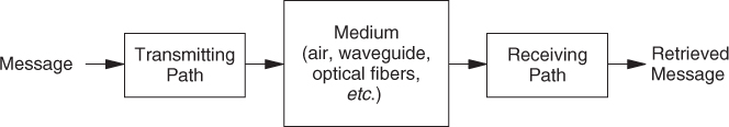
Figure 1.2 Typical analog wireless communication system.
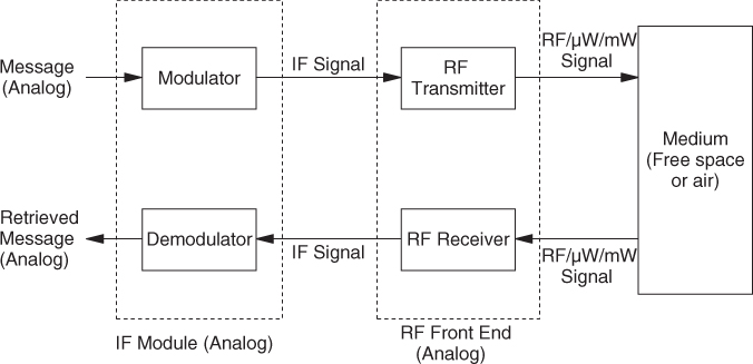
Figure 1.3 Typical digital wireless communication system.
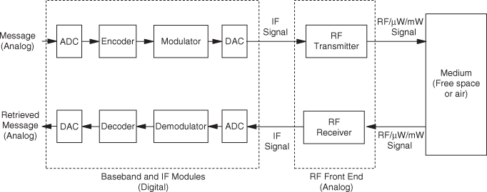
Modulation is a process of transforming the spectrum of the baseband signal to a higher frequency, called the intermediate frequency (IF). It can be used to optimize bandwidth usage and enhance the signal quality during transmission. Before transmission, the signal is moved to an even higher frequency in the RF transmitter and then sent through the channel. At the receiver, after the step down from RF, a demodulator is used to retrieve the message from the IF signal received. Both the modulator and demodulator usually work at a frequency ranging from several kilohertz to hundreds of megahertz, which is the IF range. In this frequency range, circuits and systems can be designed simply using lumped components without involving transmission-line techniques. It can be seen from Figs. 1.2 and 1.3 that modulation and demodulation can be performed either in analog or digital form. Some of the famous analog modulation schemes are amplitude modulation (AM), frequency modulation (FM), and phase modulation (PM). Today, these schemes are still being used by many commercial radio stations. As can be seen from Fig. 1.3, the digital modulator and demodulator are used in the baseband and IF modules of a digital wireless system. Digital modulation schemes such as ASK (amplitude shift keying), PSK (phase shift keying), FSK (frequency shift keying), GMSK (Gaussian minimum shift keying), and OFDM (orthogonal frequency-division multiplexing) are among the popular choices in contemporary digital wireless systems.
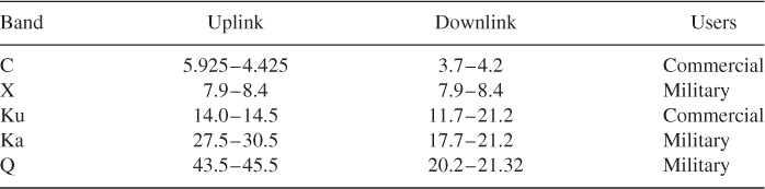
With reference to Figs. 1.2 and 1.3, for both the analog and digital wireless communication systems, the output signals of the transmitters are always continuous with frequencies in the RF, microwave (μW), or millimeter-wave (mW) ranges. This is because antennas can be used to convert the signals in these frequency ranges into electromagnetic (EM) waves for propagation in air, which is a common channel medium for wireless communications. After traveling for a long distance in the channel (either air or free space), an EM wave arrives at the receiving antenna of an RF receiver. The weak and noisy signal received is finally demodulated and decoded so that the original message signal can be retrieved. The RF transmitter and receiver are generally called the RF front end, as they work at the RF/μW/mW frequency ranges, starting from several hundred megahertz up to tens of gigahertz. Since there are many wireless signals in air, proper allocation of the frequency spectrum is needed to avoid any chaos. To this end, wireless communication protocols such as BT (Bluetooth), DECT (digital enhanced cordless communication telecommunication), GSM (global system for mobile communication), GPRS (global packet radio service), IMT-A (international mobile telecommunications–advanced), UMTS (universal mobile telecommunications system), WiBro (wireless broadband), WiMax (worldwide interoperability for microwave access), and WLAN (wireless local area network) use different parts of the frequency spectrum. The spectrum allocation charts for some commercial mobile and satellite communication systems are given in Tables 1.1 and 1.2, respectively. The same spectrum can also be used simultaneously by many users by applying additional schemes, such as TDMA (time-division multiple access) and CDMA (code-division multiple access).
Table 1.1 Frequency Bands (MHz) Allocated for Some Popular Mobile Communication Systems
| Modulation Scheme | Uplink | Downlink |
| GSM-850 | 824–849 | 869–894 |
| GSM-900 | 890–915 | 935–960 |
| GSM-1800 | 1710–1785 | 1805–1880 |
| GSM-1900 | 1850–1910 | 1930–1990 |
| UMTS | 1885–2025 | 2110–2200 |
| WiMax | 2300–2500 and 3400–3500 | |
| WiBro | 2300–2400 | |
| WLAN, Bluetooth | 2400–2480 | |
Table 1.2 Frequency Bands (GHz) Allocated for Satellite Communications
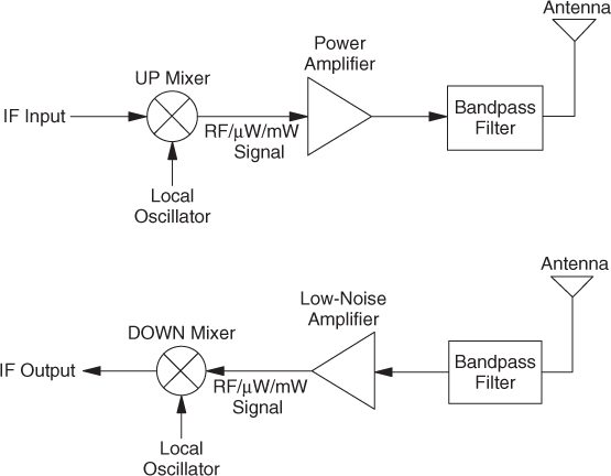
In this book we discuss only RF transmitters and receivers. The architecture of a typical one-stage unilateral RF transmitter is shown in Fig. 1.4(a). By incorporating a local oscillator (LO), the UP mixer can scale up the frequency of an IF signal. The role of the local oscillator is to impose an RF signal, usually called a carrier, onto the IF signal. Then a power amplifier is deployed for boosting the signal strength for transmission over a greater distance. With reference to Fig. 1.4(a), bandpass (image) filter has been used to remove the unwanted image signals generated by the UP mixer. Finally, through the use of a transmitting antenna, the RF signal is channeled into the air. At the unilateral RF receiver shown in Fig. 1.4(b), bandpass filter is used to remove the unwanted signals and noise picked up by the RF signal from the channel medium. A low-noise amplifier (LNA) is then inserted to magnify the signal received, which is usually weak and noisy after traveling a long distance in the channel. Finally, a local carrier signal is used to down-convert the RF signal back to IF so that it can be processed by other modules. Multiple stages can easily be cascaded to achieve better performances. For a modern wireless system, the RF front ends are required to be low loss, low cost, light weight, high performance, power efficient, and small in size.
Figure 1.4 (a) Unilateral RF transmitter; (b) unilateral RF receiver.
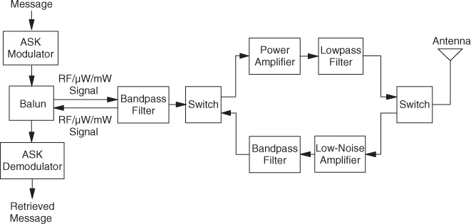
In modern wireless communication systems, the RF transmitter and receiver are often combined with a modulator and demodulator to form a single-module transceiver. The architecture of a typical bilateral transceiver (4) is shown in Fig. 1.5. Except for the antenna, all the components in a transceiver can be made easily on a single silicon chip. As a result, the antenna is usually the bulkiest component in a transceiver. It is always very desirable to have as few antennas as possible in a wireless communication system. With reference to Fig. 1.5, a switch has been employed so that an antenna can be shared by the transmitter and receiver. The preset filter here is a bandpass filter for removing channel noise. With reference to the figure, the RF modulator and demodulator here are implemented by incorporating an UP/DOWN mixer with a voltage-controlled oscillator (VCO) and a synthesizer. The two bandpass filters are to remove the unwanted frequency components. Figure 1.6 shows the functional blocks of a contemporary commercial RF transceiver (5), which is implemented using the ASK modulation scheme. The architecture is very close to that shown in Fig. 1.5. Despite the rapid advancement of semiconductor technologies, for some special applications, many components in the RF front end still remain discrete in order to achieve a high quality factor (6). Usually, microwave components such as antennas, filters, and couplers are among the bulky components which are difficult to miniaturize, as they may involve the use of various microwave resonators.
Figure 1.5 Bilateral transceiver structure. (4)
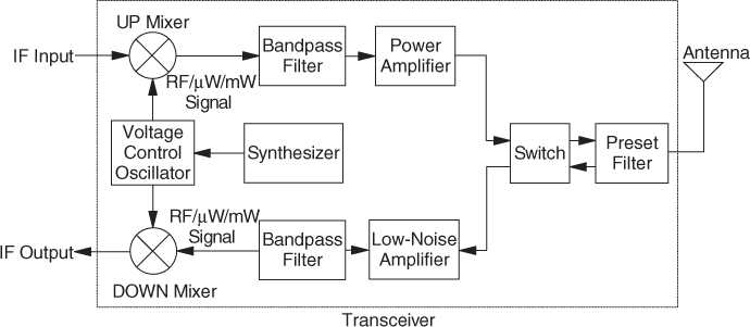
Figure 1.6 Block diagram of a commercial RF transceiver module. (5)
1.2 Microwave Components in Wireless Systems
There are two types of microwave components in the RF front end of a wireless system: active and passive. Active elements such as amplifiers, switches, oscillators, and mixers, made by employing semiconductor integrated circuit (IC) technologies, are necessary for performing power amplification and conversion. Nonlinear devices such as bipolar-junction transistors (BJTs), complementary metal–oxide semiconductors (CMOSs), and other transistors are commonly used to build these active circuits on various semiconductor materials, such as silicon, germanium, or gallium arsenide (GaAs). Nowadays, passive components such as capacitors and inductors can be easily fabricated on semiconductor substrate. For example, a capacitor can be made very compact by making use of the gate–substrate capacitance of a transistor. However, an inductor always occupies a large chip area, as it requires metallic coils to produce sufficient magnetic field (7).
Recent rapid advancement of IC fabrication processes has enabled significant size miniaturization in the RF front end. Baseband and IF modules such as encoders, decoders, modulators, and demodulators, are usually fabricated on ICs. Nevertheless, passive elements such as filters, baluns, circulators, and antennas are still difficult to miniaturize, as they are usually made on various wave-guiding resonators. Although some of these microwave components may possibly be designed by cascading lumped capacitors and inductors on a chip, it is still not easy to obtain a high Q factor, due to the lossy nature of semiconductor. As a result, they are generally made on microwave resonators for squeezing up the Q factor, which is essential for improving the frequency selectivity of the RF front end. A simple comparison of the microwave components that are made by using ICs and EM structures is shown in Table 1.3.
Table 1.3 Features of the Microwave Components That Are Made by ICs and EM Structures
| Integrated Circuits | EM Structures | |
| Circuit size | Very small (<1 mm2) (8, 9) | Large (∼cm2, depending on operating frequency) |
| Q factor | Low (<10) (10) | Very high (>100) |
| Costs | More expensive | Less expensive |
| Fabrication process | Complex | Easy |
1.3 Planar and Nonplanar Antennas in Compact Wireless Systems
An antenna is the only component in the RF front end that cannot be made simply by using lumped components, as it requires a certain physical mechanism to enable efficient electromagnetic radiation. It is well known that acceleration and deceleration in electron flows are essential for generating EM waves (11). There are many types of antennas. The most common antennas are electromagnetic radiators, which can be made on either a resonator or a traveling-wave structure. A resonating antenna has standing waves formed in its resonator. Some simple examples of resonating antennas are the monopole, dipole, aperture, and microstrip patch. On the other hand, traveling-wave antennas make use of the nonresonant voltages and currents on transmission lines to produce EM radiation. Examples of such antennas are the Beverage, Yagi–Uda, log-periodic, helix, dielectric rod, rhombic, spiral, and horn antennas. Traveling-wave antennas can also be classified as either slow-wave (surface-wave antennas) or fast-wave (leaky-wave antennas) antennas, according to the wave velocity.
1.3.1 Performance Parameters
A transmitting antenna is a device that converts alternating current (ac) into an EM wave for propagation in space. Therefore, a good antenna is not only required to have good circuit performance but must also satisfy many stringent far-field requirements (11, 12). Here, we discuss briefly some of the important design parameters for an antenna.
1.3.1.1 Antenna Bandwidth
Figure 1.7 shows the equivalent circuit of an antenna (represented by its input impedance Zant) and its interconnecting cable (with a characteristic impedance Z0 and propagation constant β) with a length of ![]() is the total input power, Pin is the power being transferred to the antenna, and Pr is the radiated power. The reflection coefficient at the antenna port is defined as
is the total input power, Pin is the power being transferred to the antenna, and Pr is the radiated power. The reflection coefficient at the antenna port is defined as
1.1 ![]()
which can easily be measured using a vector network analyzer. The power being delivered to the antenna is
1.2 ![]()
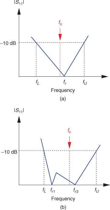
With reference to Fig. 1.8, the antenna bandwidth is usually defined as the frequency range where |S11| ≤ − 10 dB (VSWR = 2). This is also considered to be the operating frequency range of an antenna. As can be seen from the figure, fr (or fr1, fr2, … , frN for a multimode antenna) is the resonance frequency, fU is the upper bound, and fL is the lower bound of an antenna passband. For a single-mode antenna with Δf < 100%, shown in Fig. 1.8(a), either (1.3) or (1.4) can be used to determine the antenna bandwidth Δf, where the center frequency is defined as f0 = (fU + fL)/2. However, (1.3) is not suitable for a multimode antenna, which may have many resonant frequencies. The definition stated in (1.5) is another common definition used in describing the antenna bandwidth of an ultrawideband (UWB) antenna. For example, a wideband antenna covering 3.1 to 10.3 GHz has a bandwidth of 3.3:1. It is always desirable to have a wide antenna bandwidth.
Figure 1.7 Equivalent circuit of an antenna connected to a cable.
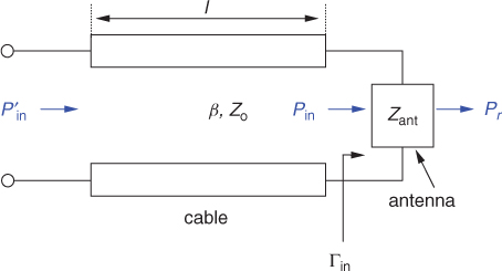
Figure 1.8 Definition of the antenna bandwidth for a radiator with (a) a single mode; (b) multiple modes.
The loss mechanism of an antenna is characterized by its unloaded quality factor (Qu), which consists of radiation loss (Qr), ohmic loss (Qc), and dielectric loss (Qd). It can be expressed as
1.6 ![]()
For an EM-wave radiating element, Qr is the dominant factor for calculating Qu. A lower Qu implies a higher radiation power Pr. As an antenna is always connected to an external circuit, the loaded QL factor is used more frequently. As can be seen from (1.7), the QL can be calculated directly from fr and Δf for a single-mode antenna:
1.7 ![]()
Antenna bandwidth (Δf) is inversely proportional to the minimum quality factor Qmin factor of an antenna. It is stated by Chu's criterion (13) that Qmin is related to the operating frequency (ko) and the radius (R) of a virtual sphere that encloses the antenna by
1.8 ![]()
1.3.1.2 Radiation Efficiency
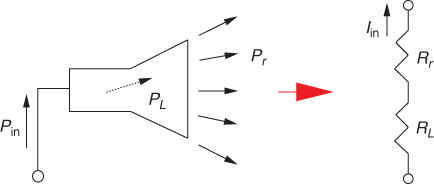
The radiation efficiency (e) is a figure of merit showing how efficient energy is being converted from input power (Pin) to output radiation (Pr).PL is the dissipative loss. With reference to Fig. 1.9, e can be described by
1.9 ![]()
The total input power can be written as Pin = Pr + PL. Assuming that the current flowing into the antenna is Iin, the radiated and dissipated powers are defined as Pr = IinRr and PL = IinRL, respectively, where Rr (radiation resistance) and RL (loss resistance) are the virtual resistors representing the radiated and dissipated powers. The values are then substituted into (1.9) to obtain
1.10 ![]()
Radiation efficiency includes both conduction and dielectric losses, which are usually not directly measurable. There are a number of methods for measuring radiation efficiency, the simplest and most widely used technique being that proposed by Wheeler in 1959, called the Wheeler cap method [14,15]. It is suitable for both single- and multimode resonating antennas (16, 17). The radiation efficiency of a small antenna can be estimated by calculating the power dissipated by an antenna (18, 19). The antenna temperature has also been used to measure the radiation efficiency (20, 21). It was recently shown that this parameter is also obtainable by discerning the time-domain response of an antenna to a short pulse (22). Various measurement methods have been compared by several authors (23, 24).
Figure 1.9 Radiated and dissipated powers of an antenna.
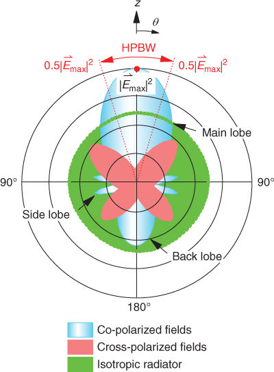
1.3.1.3 Radiation Pattern
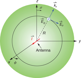
The radiation pattern describes a collective of electric (or magnetic) field strengths at a fixed distance in the far field of an antenna. Figure 1.10 shows the electric far fields radiated by an illustrative antenna placed at the origin of a spherical coordinate system ![]() . Since the antenna dimension is usually much smaller than the far-field distance (R), it can conveniently be considered to be a point source. For a simple antenna, the far-field distance is usually defined as R ≥ 2D2/λ0, where D is the largest dimension of an antenna and λ0 is the operating wavelength in air.
. Since the antenna dimension is usually much smaller than the far-field distance (R), it can conveniently be considered to be a point source. For a simple antenna, the far-field distance is usually defined as R ≥ 2D2/λ0, where D is the largest dimension of an antenna and λ0 is the operating wavelength in air.
Figure 1.10 Antenna placed at the origin of a spherical coordinate system.
According to the Poynting vector, only ![]() and
and ![]() components contribute to wave propagation in the radial direction
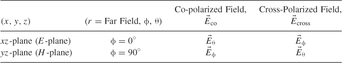
components contribute to wave propagation in the radial direction ![]() . For a symmetrical radiation pattern, the field can usually be described sufficiently by its components on the three major cut planes (xy, xz, and yz). The plane that is parallel to the vector of the maximum electric field is defined as the E-plane. Similarly, the cut plane that contains the maximum magnetic vector is called the H-plane. Consider an antenna that is equivalent to a simple electric current
. For a symmetrical radiation pattern, the field can usually be described sufficiently by its components on the three major cut planes (xy, xz, and yz). The plane that is parallel to the vector of the maximum electric field is defined as the E-plane. Similarly, the cut plane that contains the maximum magnetic vector is called the H-plane. Consider an antenna that is equivalent to a simple electric current ![]() flowing in the x-direction, Table 1.4 shows the coordinate systems of its major cut planes, along with the corresponding co- and cross-polarized fields.
flowing in the x-direction, Table 1.4 shows the coordinate systems of its major cut planes, along with the corresponding co- and cross-polarized fields.
Table 1.4 Major Cut Planes in the Radiation Pattern of an Antenna
For an antenna that has a symmetric radiation pattern with respect to the z-axis, Fig. 1.11 depicts its radiation patterns at an arbitrary cut plane ϕ = ϕ′. In the E-plane (ϕ′ = 0°), the field components ![]() and
and ![]() are the co- and cross-polarized fields, respectively. The same definition applies to the H-plane (ϕ′ = 90°), with
are the co- and cross-polarized fields, respectively. The same definition applies to the H-plane (ϕ′ = 90°), with ![]() defined as the co-polarized field and
defined as the co-polarized field and ![]() as the cross-polarized field. The definitions of some of the key parameters for a radiation pattern are now discussed. With reference to Fig. 1.11, the half-power beamwidth is the angular range in which
as the cross-polarized field. The definitions of some of the key parameters for a radiation pattern are now discussed. With reference to Fig. 1.11, the half-power beamwidth is the angular range in which ![]() . It is referred to simply as the 3-dB beamwidth. Antenna gain is defined as the ratio of the co-polarized field to that of a hypothetical isotropic radiator. The ratio between the co- and cross-polarized fields in a particular angular direction is called the cross-pole rejection. Higher rejection implies purer field polarization. For a broadside antenna with the radiation pattern shown in Fig. 1.11, the front-to-back (FB) ratio is defined as
. It is referred to simply as the 3-dB beamwidth. Antenna gain is defined as the ratio of the co-polarized field to that of a hypothetical isotropic radiator. The ratio between the co- and cross-polarized fields in a particular angular direction is called the cross-pole rejection. Higher rejection implies purer field polarization. For a broadside antenna with the radiation pattern shown in Fig. 1.11, the front-to-back (FB) ratio is defined as ![]() , where
, where ![]() is the co-polarized field in the boresight direction and
is the co-polarized field in the boresight direction and ![]() is that for the back side. A high FB ratio is very desirable for a high-gain antenna. All the aforementioned parameters vary with frequency. Directional (broadside) and omnidirectional (end-fire) antennas are among the most popular EM radiators. Directional antennas are deployed for communication systems where a distant point-to-point connectivity is desired. On the other hand, an omnidirectional antenna is used for communication in multiple directions, such as that for a hand phone.
is that for the back side. A high FB ratio is very desirable for a high-gain antenna. All the aforementioned parameters vary with frequency. Directional (broadside) and omnidirectional (end-fire) antennas are among the most popular EM radiators. Directional antennas are deployed for communication systems where a distant point-to-point connectivity is desired. On the other hand, an omnidirectional antenna is used for communication in multiple directions, such as that for a hand phone.
Figure 1.11 Radiation pattern of an antenna at the azimuthal cut plane of ϕ = ϕ′.
1.3.1.4 Polarization
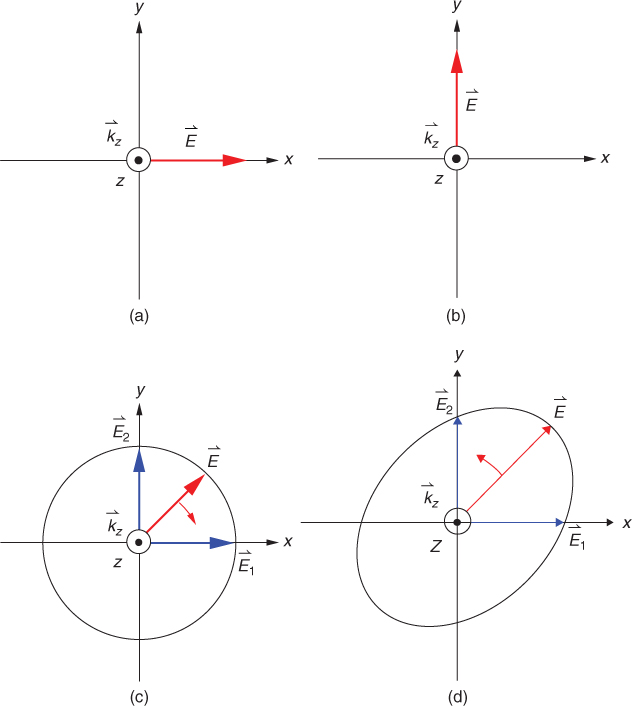
Antennas can generally be categorized as linear, circular, or elliptical polarized antennas, based on the motion of the propagating electric field with respect to time and space. Polarization matching between the transmitter and the receiver is crucial for good signal reception. With reference to Fig. 1.12(a) and 1.12(b), the plane wave propagating in the z-direction is called a linearly polarized wave, as its electric field only sweeps at all times in the x (or y)-direction (12). A circular polarized wave propagates in the z-direction with its electric field (![]() ) rotating circularly around the z-axis, as can be seen in Fig. 1.12(c). In this case,
) rotating circularly around the z-axis, as can be seen in Fig. 1.12(c). In this case, ![]() can be decomposed into two equal components,
can be decomposed into two equal components, ![]() and
and ![]() . The ratio
. The ratio ![]() is defined as the axial ratio (AR). A perfect circular polarization
is defined as the axial ratio (AR). A perfect circular polarization ![]() implies that AR = 1 (or 0 dB) and the 3-dB AR bandwidth is defined as the frequency range where AR ≤ 3 dB. When
implies that AR = 1 (or 0 dB) and the 3-dB AR bandwidth is defined as the frequency range where AR ≤ 3 dB. When ![]() , the trajectory of
, the trajectory of ![]() is an ellipse, as shown in Fig. 1.12(d). For both the circular and elliptical cases, an electric field in clockwise motion is referred to as left-handed polarization and that in anticlockwise motion as right-handed polarization.
is an ellipse, as shown in Fig. 1.12(d). For both the circular and elliptical cases, an electric field in clockwise motion is referred to as left-handed polarization and that in anticlockwise motion as right-handed polarization.
Figure 1.12 (a) Linear polarization in the x-direction; (b) linear polarization in the y-direction; (c) left-handed (clockwise) circular polarization; (d) right-handed (anticlockwise) elliptical polarization.
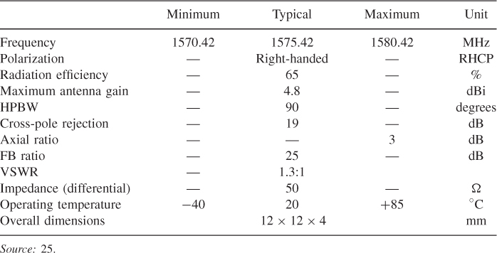
An antenna is not a stand-alone device in wireless systems. The design of an antenna is always coupled with the requirements of the entire system. It is always desirable to have an antenna that is compact, aesthetic, low profile, and light weight. Being low cost and easy to design and tune are also important design considerations that have to be taken into account. As an antenna radiates, the operation of other devices may get affected. Therefore, a good antenna must be compatible with other electronic components; most important, it is not expected to disrupt the normal operation of other systems. Mobile gadgets such as hand phones and walkie-talkies are usually placed close to the human body. In these applications, the antenna has to be designed carefully so that the body is not exposed to excessive EM radiation. The Federal Communications Commission (FCC) requires that all phones sold in the United States have an SAR (special absorption rate) ≤ 1.6 W/kg for 1 g of human tissue. In Europe, the CENELEC (European Committee for Electrotechnical Standardization) sets the SAR limit as 2 W/kg averaged over 10 g of tissue. In Table 1.5, the design specifications are given for a commercial microstrip antenna. Circular polarization is commonly used by global positioning systems (GPSs).
Table 1.5 Design Specifications for a Commercial Microstrip Patch Antenna for GPS Application
1.3.2 Planar Antennas
Planar antennas are EM radiators that are flat in shape or, at least, conform to a curved surface. This feature enables easy integration with other surface-mounted components. Microstrip patch antennas, slot antennas, planar inverted-F antennas (PIFA), planar inverted-L antennas (PILA), chip dipoles and monopoles, and suspended plate antennas (SPAs) are among the popular antennas used extensively by wireless communication systems (13, 26, 27). Figure 1.13 shows some planar antennas.
Figure 1.13 Examples of planar antennas: (a) planar dipole array; (b) circular patch; (c) microstrip patch array; (d) RFID.
1.3.3 Nonplanar Antennas
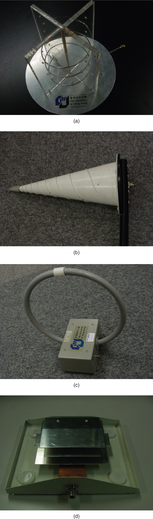
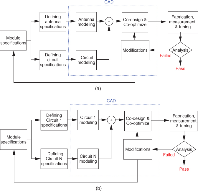
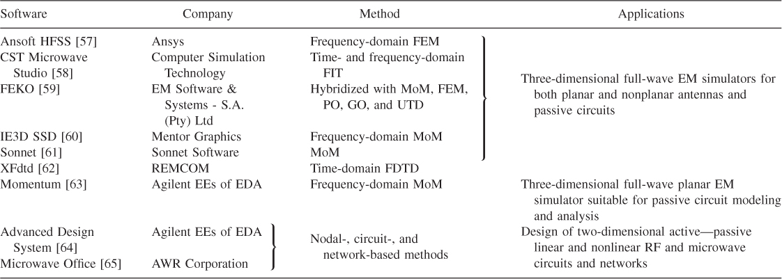
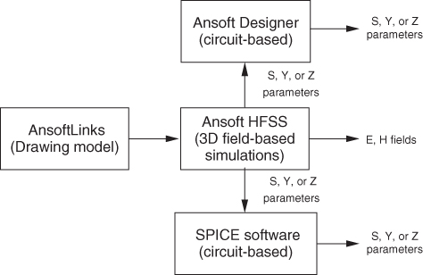
Figure 1.14 shows some of common nonplanar antennas, which are usually three-dimensional in structure [28]. Because of their bulkiness, such antennas are usually installed external to the circuit part. In many cases, nonplanar antennas require the use of reflectors, directors, impedance transformers, or multiple elements for better antenna performance. Examples of nonplanar antennas are disk antennas, horns, helixes, and reflector antennas.
Figure 1.14 Examples of nonplanar antennas: (a) helix antenna; (b) spiral antenna; (c) loop antenna; (d) monopolar-type antenna.
1.4 Multifunctional Antennas and Microwave Circuits
A multifunctional antenna is an EM radiating element that provides additional microwave functions. It is also known as an antenna-circuit module. Similarly, a multifunctional microwave circuit is one that has multiple functions in one module and is also called a circuit–circuit module.
1.4.1 Active Antennas
An active integrated antenna (AIA), being multifunctional, is an EM radiating element that provides at least one built-in function, such as amplification, equalization, oscillation, mixing, modulation–demodulation, reconfiguration, and switching (29, 30). These additional features are provided by incorporating an antenna with active devices such as diodes, switches, and various transistors. Usually, AIAs are designed without the use of matching circuits, and therefore they can be made very compact. Active antennas have been explored extensively since the 1980s for applications in spatial power combining, beam steering, and retro-directive arrays (29, 31, 32).
1.4.2 Passive Antennas
Passive integrated antennas and passive integrated circuits are very popular because of a number of advantages, such as their low loss, low cost, and high compactness. Nowadays, it is a trend to combine several microwave functions into a single module for a compact footprint (33, 34). In recent years, new components have been proposed, including the antenna filter (35), antenna circulator, antenna package (36), and balun filter (37). With the rapid advancement of packaging technologies, new design concepts, such as antenna-on-package (AOP), system-on-package (SOP), antenna-in-package (AiP), system-in-package (SiP), and low-temperature co-fired (LTCC) have been put forward. These are discussed in detail in Chapter 2.
1.5 Miniaturization Techniques for Multifunctional Antennas
Bundling several microwave functions into a single module is definitely a good way to reduce circuit size and footprint. The following techniques have frequently been used to miniaturize multifunctional antennas and microwave circuits:
1. Sharing a single resonator. Different resonances can be excited in a single resonator for designing different microwave components. Sometimes, a resonator can be used simultaneously for several functions. In general, if two microwave functions can be combined, it simply cuts down the circuit size by half. Jung and Hwang (34) made a balun and a filter on a ring resonator. In (35), the TE01δ and HEM11δ modes of a single dielectric resonator (DR) are used simultaneously for a dielectric resonator antenna and a dielectric resonator filter. It is also shown that a hollow DR can be used as a packaging cover at the same time (36).
2. Combining multiple components. Combining the resonators of several microwave devices into a single platform is a common technique used to miniaturize circuits. The devices are usually squeezed into the two surfaces of a substrate. In (37), a microstrip patch antenna and an open-ring filter are combined so that they can share the same footprint. It was shown that a balun can be placed on the substrate underside of a printed dipole (38) to form a compact RF module.
3. Applying multilayer technology. Modern packaging techniques enable easy fabrication of various multilayer configurations. AOP, AiP, SOP, SiP, and LTCC are among the popular technologies used for packing multiple microwave components into multilayer packages (39, 40). In principle, the entire RF front end can be made into different layers of a single package. For these configurations, antennas are usually stacked on top of the packages to enable EM radiation.
4. Integrating into substrate. Recently, substrate integration technology has been widely used in the design of both active and passive multifunctional modules in the millimeter-wave range. In (41), a substrate integrated waveguide (SIW) cavity-backed slot antenna oscillator is proposed. Using a half-mode SIW, Cheng et al. (42) proposed a quadri-polarized frequency scanning antenna built by combining a 3-dB coupler and a leaky-wave antenna array.
5. Removing matching circuits. This technique is used frequently by amplifying antennas (43). On the receiver side, the active low-noise amplifying antenna usually does not contain any input-matching circuit. On the transmitter side, a power-amplifying antenna works without having an output-matching circuit (44). Removal of part of the peripheral circuit helps to cut down the component size and signal path.
6. Multitasking the microwave element. For the design of antenna oscillators, the antenna can be used simultaneously as the resonator, load (45), and feedback element (46) of an oscillator. Squeezing multiple tasks into a microwave element can reduce the circuit size significantly.
1.6 Design Processes and Considerations
Some topics pertaining to antenna–circuit modules have been covered by Gupta and Hall (47). Recently, the rapid advancement in computer-aided design (CAD) tools, along with the availability of more powerful computers, has significantly shortened the design cycle of multifunctional antennas and microwave circuits (48). Designing a multifunctional component usually involves co-designing and co-optimizing several microwave functions. Flow diagrams depicting the design processes are shown in Fig. 1.15. CAD tools can be used in many ways to assist in the design process. For an antenna–circuit module, the antenna and circuit are usually designed separately, as they may require different modeling approaches. The calculation of antenna far fields requires full-wave analysis, such as the moment method (MoM), the finite integral technique (FIT), the finite-element method (FEM), the time-domain finite-difference method (FDTD), geometric optics (GO), physical optics (PO), and the uniform theory of diffraction (UTD). On the other hand, circuit- and network-based methods, such as nodal analysis, the transmission matrix, and harmonics balance, are frequently used to analyze both active and passive circuits. Over the past two decades, much effort has been devoted to developing various optimization algorithms for microwave applications. The genetic algorithm (49, 50), particle swarm (51, 52), and neural network (53) are among the popular optimization algorithms frequently incorporated with various computational EM tools to expedit the optimization process. Recently, stochastic methods (54, 55) have also been explored for optimizing complex EM problems.
Figure 1.15 Design procedures of multifunctional integrated circuits: (a) antenna–circuit module; (b) circuit–circuit module.
Despite the availability of many powerful CAD tools, combining antennas with circuits still requires special care, as the joint simulation model can become very large and complex. In computer modeling, there is always a trade-off between completeness and accuracy. A complete full-wave model is good for accuracy, but it requires many more computational resources and a longer simulation time. In contrast, a simplified model is easily manageable by computers, but at the expense of accuracy. To expedite the simulation time, it is also not uncommon to omit the coupling effects of antenna-to-antenna and antenna-to-circuit connections. This can again introduce errors in the computation.
1.7 Design Tools and Software
Today, many CAD softwares, usually adorned with colorful and user-friendly graphic user interfaces, are commercially available for modern RF and microwave designs. They are commonly used to reduce the design-to-product time. In general, there are two types of microwave CAD tools: network (or circuit)- and field-based. An early software program was SPICE (simulation program with integrated-circuit emphasis). In the 1970s, computerized design tools were less common, and most of microwave design programs were encoded in computer programs or punch cards, often owned by large IC manufacturers and customized only for certain transistors. For example, SPEEDY was developed by Les Besser for Fairchild, and CAIN-01 was written by R. P. Coats for Texas Instruments. In 1973, Besser introduced the first commercially available CAD software, called COMPACT (computer optimization of microwave passive and active circuits), for designs of various microwave circuits (56). It was later converted into SuperCOMPACT and became an industrial standard at that time.
Since then, a 40-year period of computer development has brought CAD technology to another height. Some commonly used commercial EM software is compared in Table 1.6. Today, many complex linear and nonlinear circuits, such as filters, couplers, amplifiers, oscillators, and mixers, can easily be modeled using two-dimensional SPICE software, which is supported by a vast number of device libraries. As can be seen in the table, many three-dimensional full-wave tools are also available for simulating field distributions of antennas and EM structures.
Table 1.6 Comparison of Some Commercially Available RF and Microwave Design Softwares
The co-design and co-optimization processes may require the use of multiple CAD tools. The system outputs of a microwave structure (either a passive circuit or an antenna), which are usually simulated using a three-dimensional full-wave software, can usually be exported to circuit- and network-based CAD tools for co-simulations. As an example, it was shown by Lim et al. (33) that the reflection coefficient S11 (or input impedance Zin) of an antenna can be imported directly into the AWR Microwave Office as a subcircuit module for combination with other devices. Today, many advanced three-dimensional full-wave EM softwares, such as
Ansoft HFSS and CST Microwave Studio, have their own built-in circuit-based simulators. Figure 1.16 shows the co-simulation platform for a series of Ansoft EM software (57). As can be seen, the outputs (S, Y, or Z parameters) of an antenna (Ansoft HFSS) can easily be exported internally to the Ansoft Designer (circuit-based) or externally to another SPICE simulator for joint simulations. This simplifies the design processes of multifunctional antennas and circuits significantly.
Figure 1.16 Simulation platform for Ansoft EM simulators. (57)
1.8 Overview of the Book
This book encompasses multifunctional antennas and microwave components, along with their design methods. Recent developments and important design issues are also discussed. In this book, multiple design tools and softwares are used jointly for the design of multifunctional components which may contain both active and passive devices. To facilitate the reading, a brief overview of this book is provided here.
Chapter 2 presents several new multifunctional passive integrated antennas and passive integrated circuits, such as an antenna filter, antenna package, and balun filter. Dielectric resonators and microstrip-based resonators are used to demonstrate the design ideas. In most cases, multiple functions are implemented on a piece of single resonator for a compact footprint. With the use of field-based and SPICE softwares, design procedures for several multifunctional modules are described in detail.
In Chapter 3 it is shown that antennas can be made reconfigurable by integrating switches into the radiation aperture. Frequency, pattern, and multiple reconfigurations are implemented using patch and fractal antennas. A pattern reconfigurable leaky wave antenna is also shown. Some recent work conducted at the Institute of Applied Physics, University of Electronic Science and Technology of China, Chengdu, is described.
Chapter 4 explores low-noise amplifying antennas. In the first part, a wearable active antenna made on a textile is described. It is shown that low-noise amplifiers can be designed without using an input matching circuit. Also, matching techniques are included.
Reflection-amplifier and coupled-load antenna oscillators are visited in Chapter 5. A number of design examples are given along with their design procedures. It is shown that reasonable phase noise and high output power are achievable in both types of antenna oscillators.
In Chapter 6, the recent development of solar-cell-integrated antennas is reviewed. Several new antenna configurations are covered. Dielectric resonator antennas and suspended plate antennas are examined to demonstrate the design ideas. Solar cells can be used in the future to provide self-sustaining power to wireless communication systems.
References
1. A. G. Bell, “Improvement in telephony,” U.S. patent 174,465, Mar. 7, 1786.
2. K. C. Kao and G. A. Hockham, Dielectric-fibre surface waveguides for optical frequencies, IEE Proc., vol. 133, no. 3, pp. 191–198, June 1986. (Originally published in the same journal in 1966.)
3. http://en.wikipedia.org/wiki/Encoder.
4. K. Feher, Wireless Digital Communications: Modulation and Spread Spectrum Applications. Upper Saddle River, NJ: Prentice Hall, 1995.
5. Datasheet: RFW3M-PA Transceiver Module, Vishay RF Waves, Feb. 2009.
6. M. Steer, Microwave and RF Design: A Systems Approach. Raleigh, NC: SciTech, 2009.
7. H. Moon, J. Han, S. Choi, D. Keum, and B. Park, An area-efficient 0.13-μm CMOS multiband WCDMA/HSDPA receiver, IEEE Trans. Microwave Theory Tech., vol. 58, pt. 2, pp. 1447–1455, May 2010.
8. S. S. K. Ho and C. E. Saavedra, A CMOS broadband low-noise mixer with noise cancellation, IEEE Trans. Microwave Theory Tech., vol. 58, pp. 1126–1132, May 2010.
9. P. Mak and R. P. Martins, A 2 × VDD-enabled mobile-TV RF front-end with TV-GSM interoperability in 1-V 90-nm CMOS, IEEE Trans. Microwave Theory Tech., vol. 58, pp. 1664–1676, July 2010.
10. C. Lee, T. Chen, J. D. Deng, and C. Kao, A simple systematic spiral inductor design with perfected Q improvement for CMOS RFIC application, IEEE Trans. Microwave Theory Tech., vol. 53, pp. 523–528, Feb. 2005.
11. C. A. Balanis, Antenna Theory Analysis and Design, 2nd ed. New York: Wiley, 1997.
12. J. D. Kraus and R. J. Marhefka, Antennas for All Applications, 3rd ed. New York: McGraw-Hill, 2003.
13. Z. N. Chen and M. Y. W. Chia, Broadband Planar Antennas: Design and Applications. Chichester, UK: Wiley, 2006.
14. H. Wheeler, The radiansphere around a small antenna, Proc. IRE, vol. 47, no. 8, pp. 1325–1331, Aug. 1959.
15. G. Smith, An analysis of the Wheeler method for measuring the radiating efficiency of antennas, IEEE Trans. Antennas Propag., vol. 25, no. 4, pp. 552–556, July 1977.
16. H. Choo, R. Rogers, and H. Ling, On the Wheeler cap measurement of the efficiency of microstrip antennas, IEEE Trans. Antennas Propag., vol. 53, pp. 2328–2332, July 2005.
17. C. Cho, I. Park, and H. Choo, A modified Wheeler cap method for efficiency measurements of probe-fed patch antennas with multiple resonances, IEEE Trans. Antennas Propag., vol. 58, pp. 3074–3078, Sept. 2010.
18. R. H. Johnston and J. G. McRory, An improved small antenna radiation-efficiency measurement method, IEEE Antennas Propag. Mag., vol. 40, pp. 40–48, Oct. 1998.
19. W. L. Schroeder and D. Gapski, Direct measurement of small antenna radiation efficiency by calorimetric method, IEEE Trans. Antennas Propag., vol. 54, pp. 2646–2656, Sept. 2006.
20. J. Ashkenazy, E. Levine, and D. Treves, Radiometric measurement of antenna efficiency, Electron. Lett., vol. 21, no. 3, pp. 111–112, Jan. 1985.
21. N. J. McEwan, R. A. Abd-Alhameed, and N. Z. Abidin, A modified radiometric method for measuring antenna radiation efficiency, IEEE Trans. Antennas Propag., vol. 51, pp. 2099–2105, Aug. 2003.
22. A. Khaleghi, Time-domain measurement of antenna efficiency in reverberation chamber, IEEE Trans. Antennas Propag., vol. 57, pp. 817–821, Mar. 2009.
23. D. M. Pozar and B. Kaufman, Comparison of three methods for the measurement of printed antenna efficiency, IEEE Trans. Antennas Propag., vol. 36, pp. 136–139, Jan. 1988.
24. E. H. Newman, P. Bohley, and C. H. Walker, Two methods for the measurement of antenna efficiency, IEEE Trans. Antennas Propag., vol. 23, pp. 457–461, July 1975.
25. Datasheet: MPA1575D124 Compact Microstrip Patch Antenna GPS L1 Band, Maxtenna Antenna Innovations Company.
26. K. L. Wong, Compact and Broadband Microstrip Antennas. Hoboken, NJ: Wiley, 2002.
27. K. L. Wong, Planar Antennas for Wireless Communications. Hoboken, NJ: Wiley, 2003.
28. K. L. Wong, Design of Nonplanar Microstrip Antennas and Transmission Lines. New York: Wiley, 1999.
29. J. A. Navarro and K. Chang, Integrated Active Antennas and Spatial Power Combining. New York: Wiley, 1996.
30. M. Steer and W. D. Palmer, Eds., Multifunctional Adaptive Microwave Circuits and Systems. Raleigh, NC: SciTech, 2009.
31. A. Mortazawi, T. Itoh, and J. Harvey, Active Antennas and Quasi-optical Array. Piscataway, NJ: IEEE Press, 1999.
32. R. A. York and Z. B. Popovic, Active and Quasi-optical Arrays for Solid-State Power Combining. New York: Wiley, 1997.
33. E. H. Lim, K. W. Leung, and X. S. Fang, The compact circularly-polarized hollow rectangular dielectric resonator antenna with an underlaid quadrature coupler, IEEE Trans. Antennas Propag., vol. 59, pp. 288–293, Jan. 2011.
34. M. Jung and H. Hwang, A balun-BPF using a dual mode ring resonator, IEEE Microwave Guided Wave Lett., vol. 7, pp. 652–654, Sept. 2007.
35. E. H. Lim and K. W. Leung, Use of the dielectric resonator antenna as a filter element, IEEE Trans. Antennas Propag., vol. 56, pp. 5–10, Jan. 2008.
36. E. H. Lim and K. W. Leung, Novel application of the hollow dielectric antenna as a packaging cover, IEEE Trans. Antennas Propag., vol. 54, pp. 484–487, Feb. 2006.
37. Y. J. Sung, Microstrip resonator doubling as a filter and as an antenna, IEEE Antennas Wireless Propag. Lett., vol. 8, pp. 486–489, Mar. 2009.
38. E. Avila-Navarro, J. Anton, J. M. Blanes, and C. Reig, Broadband printed dipole with integrated via-hole balun for WIMAX applications, Microwave Opt. Tech. Lett., vol. 53, no. 1, pp. 52–55, Jan. 2011.
39. Y. P. Zhang and D. Liu, Antenna-on-chip and antenna-in-package solutions to highly integrated millimeter-wave devices for wireless communications, IEEE Trans. Antennas Propag., vol. 57, pp. 2830–2841, Oct. 2009.
40. R. Li, G. DeJean, M. Maeng, K. Lim, S. Pinel, M. Tentzeris, and J. Laskar, Design of compact stacked-patch antennas in LTCC multilayer packaging modules for wireless applications, IEEE Trans. Adv. Packag., vol. 27, pp. 581–589, Nov. 2004.
41. F. Giuppi, A. Georgiadis, A. Collado, M. Bozzi, and L. Perregrini, Tunable SIW cavity backed active antenna oscillator, Electron. Lett., vol. 46, no. 15, July 2010.
42. Y. J. Cheng, W. Hong, and K. Wu, Millimeter-wave half mode substrate integrated waveguide frequency scanning antenna with quadri-polarization, IEEE Trans. Antennas Propag., vol. 58, pp. 1848–1855, June 2010.
43. D. Segovia-Vargas, D. Castro-Galán, L. E. García-Mu noz, and V. González-Posadas, Broadband active receiving patch with resistive equalization, IEEE Trans. Microwave Theory Tech., vol. 56, pp. 56–64, Jan. 2008.
44. G. A. Ellis and S. Liw, Active planar inverted-F antennas for wireless applications, IEEE Trans. Antennas Propag., vol. 51, pp. 2899–2906, Oct. 2003.
45. E. H. Lim and K. W. Leung, Novel utilization of the dielectric resonator antenna as an oscillator load, IEEE Trans. Antennas Propag., vol. 55, pp. 2686–2691, Oct. 2007.
46. K. Chang, K. A. Hummer, and G. K. Gopalakrishnan, Active radiating element using FET source integrated with microstrip patch antenna, Electron. Lett., vol. 24, pp. 1347–1348, Oct. 1988.
47. K. C. Gupta and P. S. Hall, Analysis and Design Integrated Circuit Antenna Modules. Hoboken, NJ: Wiley, 2000.
48. H. J. Visser, Approximate Antenna Analysis for CAD. Chichester, UK: Wiley, 2009.
49. A. Hoorfar, Evolutionary programming in electromagnetic optimization: a review, IEEE Trans. Antennas Propag., vol. 55, pp. 523–537, Mar. 2007.
50. J. J. Sun, D. S. Goshi, and T. Itoh, Optimization and modeling of sparse conformal retrodirective array, IEEE Trans. Antennas Propag., vol. 58, pp. 977–981, Mar. 2010.
51. N. Jin and Y. Rahmat-Samii, Parallel particle swarm optimization and finite-difference time-domain (PSO/FDTD) algorithm for multiband and wide-band patch antenna designs, IEEE Trans. Antennas Propag., vol. 53, pp. 3459–3468, Nov. 2005.
52. S. Genovesi, A. Monorchio, R. Mittra, and G. Manara, A sub-boundary approach for enhanced particle swarm optimization and its application to the design of artificial magnetic conductors, IEEE Trans. Antennas Propag., vol. 55, pp. 766–770, Mar. 2007.
53. Y. Kim, S. Keely, J. Ghosh, and H. Ling, Application of artificial neural networks to broadband antenna design based on a parametric frequency model, IEEE Trans. Antennas Propag., vol. 55, pp. 669–673, Mar. 2007.
54. Z. Li, Y. E. Erdemli, J. L. Volakis, and P. Y. Papalambros, Design optimization of conformal antennas by integrating stochastic algorithms with the hybrid finite-element method, IEEE Trans. Antennas Propag., vol. 50, pp. 676–684, May 2002.
55. W. Weng, F. Yan, and A. Z. Elsherbeni, Linear antenna array synthesis using Taguchi's method: a novel optimization technique in electromagnetics, IEEE Trans. Antennas Propag., vol. 55, pp. 723–730, Mar. 2007.
56. L. Besser, A fast computer routine to design high frequency circuits, IEEE ICC Conference, San Francisco, June 1970.
57. http://www.ansoft.com/products/hf/hfss/.
60. http://www.mentor.com/electromagnetic-simulation/.
61. http://www.sonnetsoftware.com/.
62. http://www.remcom.com/xf7.
63. http://www.home.agilent.com/agilent/product.jspx?nid=-34333.804583.00&lc=eng&cc=HK.