
Chapter 5
Oscillating Antennas
5.1 Introduction
A microwave oscillator is a device that converts direct-current (dc) energy into alternating-current (ac) energy (1). In modern wireless systems, microwave oscillators are commonly used to generate carrier signals for radio transmitters. At RF receivers, oscillators are usually associated with mixers and phase-locked loops for extracting message signals. For decades, active devices such as Gunn diodes, impact ionization avalanche transit time (IMPATT) devices, and resonant tunneling diodes (RTDs) have been used broadly to perform this important dc-to-ac conversion. Bipolar-junction transistors (BJT), metal–semiconductor field-effect transistors (MESFET), metal-oxide-semiconductor field-effect transistors (MOSFET), and high-electron-mobility transistors (HEMT) (2) are among the modern transistors in common use in the design of various oscillator circuits.
In past decades, oscillators were integrated with antennas mainly for spatial power combining (1, 3). This is because a microstrip is extremely lossy in the millimeter-wave ranges, while, on the other hand, a spatial power combining has relatively lower loss. An oscillating antenna, also called an antenna oscillator, is a multifunctional circuit that can be designed easily by employing an antenna simultaneously as the resonator, the feedback element, and as the load of an oscillator. In this chapter, design examples are given for all the aforementioned cases.
5.2 Design Methods for Microwave Oscillators
There are many ways to design a microwave oscillator. In this section, attention is given to S parameters and the network model since most antenna oscillators can be analyzed conveniently using these two methods.
5.2.1 Design Using S Parameters
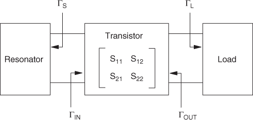
Design using S parameters has already been well covered by many research papers and textbooks (2, 4–6). We discuss only briefly the design procedure of an oscillator based on the small-signal S parameters. Figure 5.1 shows the block diagram of a transistor oscillator. At a certain biasing point, the transistor can be represented by its small-signal S parameters, which are all frequency-dependent variables. For a transistor, the necessary oscillation conditions are given as follows.
5.1 ![]()
5.2 ![]()
where
5.3.1 ![]()
5.3.2 ![]()
5.3.3 ![]()
Elaborating ΓINΓS in (5.2), we get
5.4 ![]()
As can be seen from 5.3, the only conditions that make ΓINΓS = 1 are RIN = − RS and XIN = − XS, leading to the following alternative conditions for oscillation:
5.5 ![]()
Also, it can be shown that the condition ΓOUTΓL = 1 in (5.2) is equivalent to the following oscillating conditions:
5.6 ![]()
In brief, the oscillation conditions (5.1) and (5.2) imply (5.5) and (5.6). A complete description of the oscillator theory is available (7).
Figure 5.1 Block diagram of a transistor oscillator.
5.2.2 Design Using a Network Model
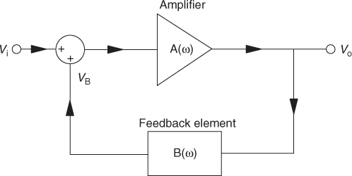
Amplifiers require a transistor to have K > 1, which is exactly opposite to the requirement for an oscillator. From theory, the same transistor can be used for oscillator design if certain instability is introduced to the amplifier, making K < 1. This can be done easily by introducing a positive feedback network to an amplifier. Traditionally, this type of oscillating circuit can best be described and analyzed using network theory (5, 6). Figure 5.2 shows the network representation of an oscillator circuit. Assuming that the amplifier has a gain of A(ω) and the feedback element provides a positive gain of B(ω), the transfer function of the network can be written
5.7 ![]()
For oscillation to occur, the output Vo must exist even when no input signal Vi is applied. This is possible only when 1 − B(ω)A(ω) = 0, leading to the well-known Barkhausen criterion B(ω)A(ω) = 1. It implies that the loop gain must be unity for oscillation to occur. To make B(ω)A(ω) = 1, the phase shift around the closed loop must be 0° or in multiples of 360° at the oscillating frequency.
Figure 5.2 Network model of an oscillator.
5.2.3 Specifications of Microwave Oscillators
An oscillator is usually named for the type of resonator it employs. Cavity, dielectrics, microstrip, and yittrium–iron–garnet (YIG) are among the popular resonators used by oscillators. In general, the design requirements for a microwave oscillator are as follows:
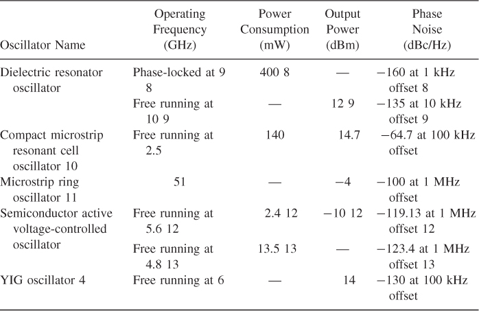
Table 5.1 shows some contemporary oscillators, along with their reported power consumption, output power, and phase noise performance. To design a good microwave oscillator, a high Q factor is always needed for lower phase noise. This can be achieved by incorporating a high-Q resonator and, of course, the use of other high-Q components. Phase-locked loops can be used to improve the oscillator phase noise. It can be seen from Table 5.1 that the phase noise of a phased-locked DRO is higher than that for a free-running DRO. Microstrip oscillators do not have low phase noise, as the Q factor of a microstrip resonator is usually low. Nowadays, having low power consumption and compact size are also important to the design of microwave oscillators. Semiconductor oscillators usually have low power consumption as well as low output power.
Table 5.1 Performance of Some Contemporary Microwave Oscillators
5.3 Recent Developments and Issues of Antenna Oscillators
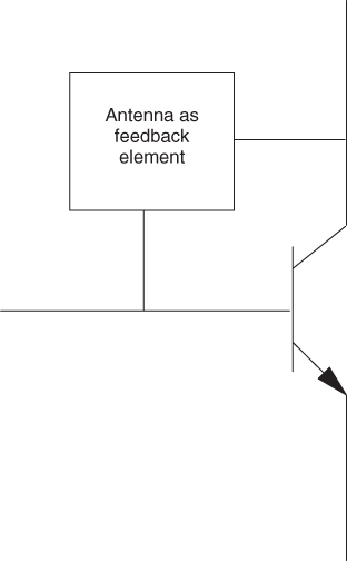
Most of the antenna oscillators reported make simultaneous use of the antenna as a resonator, a load, or a feedback element. In most cases, the antenna itself has double functions. When an antenna is used as a resonator or a load, the integrated circuit is called a reflection-amplifier antenna oscillator. Active devices such as the BJT and FET have been broadly deployed for such designs. For ease of explanation, a BJT is used to describe all subsequent design examples. As can be seen in Figs. 5.3 and 5.4, a transistor can be configured into either a common-base (or common-gate) or common-emitter (or common-source) biasing scheme in such an antenna oscillator. For such designs, S-parameter analysis is the most intuitive approach. On the other hand, if the antenna is used as a feedback element, as shown in Fig. 5.5, the new device is then called a coupled-load antenna oscillator. In this case it can easily be designed and described using the network model.
Figure 5.3 Common-base antenna oscillators with (a) an antenna as the oscillator resonator; (b) an antenna as the oscillator load.
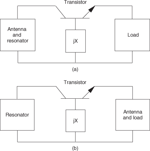
Figure 5.4 Common-emitter antenna oscillators with (a) an antenna as the oscillator resonator; (b) an antenna as the oscillator load.
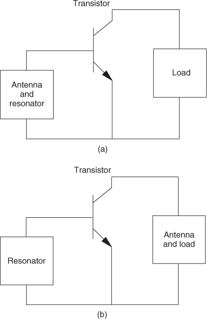
Figure 5.5 Configuration of the coupled-load antenna oscillator where the antenna acts as a feedback load.
A good antenna oscillator should have low phase noise, high transmitting power, and broad tunable frequency. The phase noise performance of an antenna oscillator is determined by its Q factor, which is inversely proportional to the total loss of the antenna and oscillator circuit. Antenna oscillators usually have high phase noise. This is because the total Q factor of an antenna oscillator is limited by its radiating antenna, whose Q factor is usually low, a condition necessary for high antenna radiation efficiency and a broad impedance bandwidth. Obviously, the design of an oscillating antenna is always a trade-off between optimizing the oscillator phase noise, antenna radiation efficiency, and antenna bandwidth. The transmitting power of an antenna oscillator is determined by the output power, linearity, and impedance matching of the active device being employed. It is usually below 25%. Rapid advancement in silicon technology has made possible the use of high-power transistors in designing various antenna oscillators in the millimeter-wave ranges. Like oscillators, oscillating antennas should have a wide frequency tuning range. To achieve this, a tunable voltage-controlled varactor can be used to change the operating frequency of an antenna oscillator.
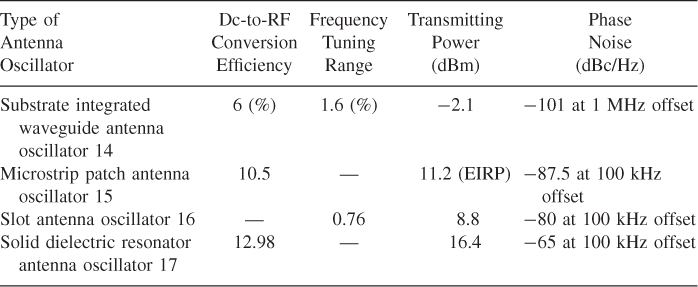
In Table 5.2 we compare the performances of some recently reported antenna oscillators. Comparing it with Table 5.1, it is obvious that the phase noise of antenna oscillators is higher than for isolated oscillators. Over the past few years, much effort has been made to reduce the phase noise of antenna oscillators. For example, the phase noise of an antenna oscillator can be improved by using an embedded (−101.5 dBc/Hz at 100 kHz offset (17)) or a backing (−96 dBc/Hz at 100 kHz offset (18, 19)) cavity. It has also been found that low phase noise could be obtained by phase- or injection-locking the oscillating antennas (−98 dBc/Hz at 10 kHz offset (20)), at the expense of having a more complex circuit configuration.
Table 5.2 Performance of Some Recently Reported Antenna Oscillators
5.4 Reflection-Amplifier Antenna Oscillators
In this section, reflection-amplifier oscillating antennas are discussed. In the first part, a BJT oscillator is combined with a DRA for designing a dielectric resonator antenna oscillator (DRAO). A differential quasi-Yagi antenna oscillator is then explored in the second part. For both cases, the antenna serves as both the radiating element and oscillator load. Finally, a trifunction DRAO, which has an embedded metallic cavity and a better phase noise, is discussed.
5.4.1 Rectangular DRAO
5.4.1.1 Configuration
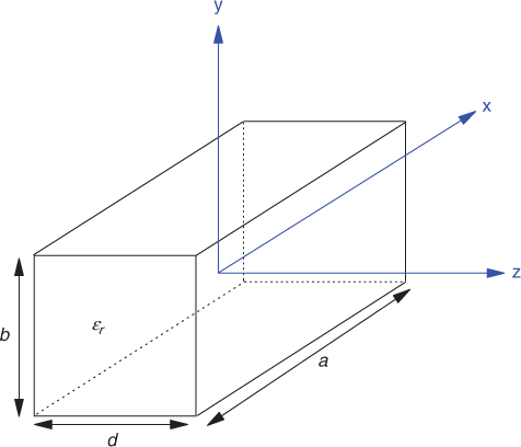
A reflection-amplifier DRAO is designed using S parameters. Here, a DR is used simultaneously as the antenna and the oscillator load (17). The schematic diagram of the common-base and one-port antenna oscillator configuration is shown in Fig. 5.6, where an Infineon BFP420 transistor is used as the active device. As discussed in Section 5.2.1, the circuit oscillates at a particular frequency at which Xin + XL = 0 and |Rin| > RL. A solid rectangular DRA is used. With reference to Fig. 5.7, the dimensions a, b, and d of the rectangular DRA (with dielectric constant of ε r) can be determined using the transcendental equation, exciting in its TE![]() mode (21):
mode (21):
5.8 ![]()
where
5.9.1 ![]()
5.9.2 ![]() kx, ky, and kz represent the wavenumbers in the x-, y-, and z-directions, respectively and k0 is the free-space wavenumber at resonance frequency.
kx, ky, and kz represent the wavenumbers in the x-, y-, and z-directions, respectively and k0 is the free-space wavenumber at resonance frequency.
Figure 5.6 Schematic of a reflection-amplifier DRAO.
Figure 5.7 Dimensions of an isolated rectangular solid DRA.
This DRA is then used in designing the DRAO. Figure 5.8 shows the configuration of the DRAO. The DR has a length of L = 52.2 mm, a width of W = 42.4 mm, a height of H = 26.1 mm, and a dielectric constant of ε r = 6. It is excited by a microstrip-fed aperture of length La = 0.3561λe and Wa = 2 mm, where ![]() is the effective wavelength in the aperture. Duroid substrates of dielectric constant ε r = 2.94 and d = 0.762 mm were used for all the circuits.
is the effective wavelength in the aperture. Duroid substrates of dielectric constant ε r = 2.94 and d = 0.762 mm were used for all the circuits.
Figure 5.8 Rectangular solid DRAO excited by a microstripline-fed aperture: (a) side view; (b) top view. (From (17), copyright © 2007 IEEE, with permission.)
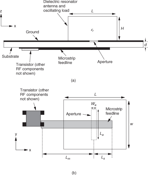
As can be seen in Fig. 5.8, the emitter output of the transistor was soldered to the 50-Ω microstrip feedline which was used to feed the antenna. The feedline was extended with a length of Lm = 40 mm and a matching stub of Ls = 9.5 mm was used. A finite ground plane of size 20 × 20 cm2 was used in both the simulations and experiments for the DRAO. In the simulation and optimization processes, the DRA in Fig. 5.6 was replaced by a 50-Ω resistive load. After optimization, the resistor was then replaced by the actual antenna. This is feasible because the input impedance of the DRA can be approximated by a resistive load (50 Ω in this case) at resonance.
5.4.1.2 Measurement Method
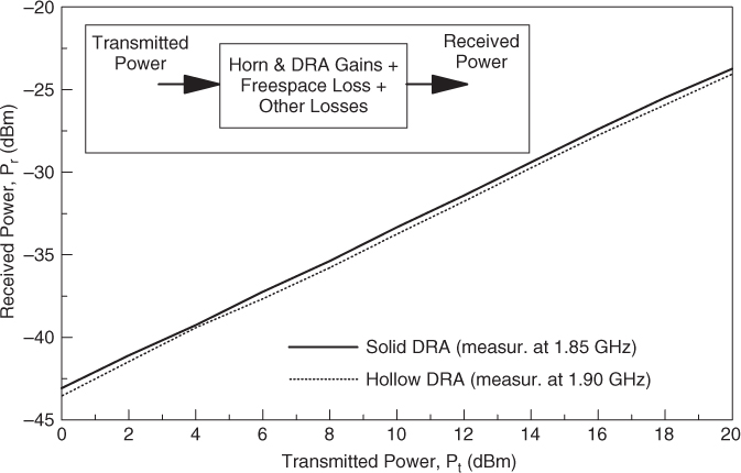
In this section we explore the use of the compact-range anechoic chamber for measuring active antennas. Here, the HP85301CK02 receiving-mode compact-range antenna measurement system (22) was used to measure the DRAO, in the arrangement shown in Fig. 5.9. The distances are D1 = 4.5 m and D2 = 2.5 m to ensure that the far-field requirement is satisfied at 1.85 GHz, where the side-feed receiving horn antenna has an antenna gain of Gr = 7.36 dBi. To calibrate the measurement system, the passive rectangular solid DRA was first placed at the center of the rotator. It was then supplied with a 1.85-GHz monotonic signal with various power levels. In the measurements, the monotonic testing signal was generated by an Agilent E8244A signal generator, and the received power was recorded at the receiving end. Figure 5.10 shows the curve that relates the transmitted and received powers of the passive rectangular solid DRA. The curve of a passive hollow DRA (which is supplied with a 1.90-GHz monotonic signal and will be used for designing the trifunction DRA later) is also given in the figure. The calibration has taken into account all of the gains and losses, including the horn gain, DRA gain, free-space loss, and other losses, as depicted in the inset. Since the output power of the signal generator is known for the passive DRA, the DRAO output power can be determined by comparing the received power from the DRAO directly to that from the passive DRA.
Figure 5.9 Modified compact-range measurement setup for active transmitting antennas. (From (17), copyright © 2007 IEEE, with permission.)
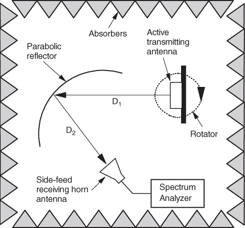
Figure 5.10 Relationships between the transmitted and received powers for the passive solid DRA in Fig. 5.8 and the passive hollow DRA in Fig. 5.15. (From (17), copyright © 2007 IEEE, with permission.)
5.4.1.3 Results and Discussion
The antenna part of the DRAO was measured using an HP8510C network analyzer, and an HP8595E spectrum analyzer was used to characterize the oscillation performance of the DRAO. In experiment, the BFP420 transistor is biased at VCE = 2.2 V and IC = 27 mA, with biasing resistors of R1 = 390 Ω and R2 = 47 Ω. The dc biasing voltages are V1 = 12.42 V and V2 = − 2 V. A dc block and two RF chokes are used. Before being connected to the DRA, the oscillator was optimized experimentally with a 50-Ω resistor. An inductive load of X = j59.68 Ω (L = 5.1 nH) was used to destabilize the transistor, with a capacitor of C = 6 pF terminated at the collector port. The Eccostock HiK Powder with dielectric constant ε r = 6 was used as the dielectric material. A few hard-form clad boards ( ε r ∼ 1) were used to construct a rectangular container for the powder, which is fine granular and free flowing. It was found that slight jogging is sufficient to even the powder in the container and no further processing is required.
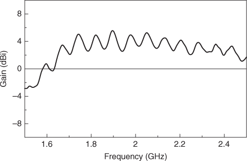
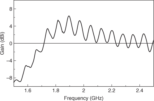
Ansoft HFSS software was used in the following simulations. Figure 5.11 shows the simulated and measured reflection coefficients shown as a function of frequency for the passive solid DRA in Fig. 5.8. The corresponding impedances are given in the inset. As can be seen from the figure, a wide measured impedance bandwidth of 22.14% is obtained. The measured resonance frequency is 1.86 GHz, which agrees well with the simulated value of 1.83 GHz (1.47% error). By using the compact-range measurement method described in this section, the measured spectrum of the free-running active DRAO is shown in Fig. 5.12. With reference to the figure, a stable oscillation of a received power level of Pr = − 27.04 dBm is observed at 1.878 GHz with a clean spectrum. Using Fig. 5.10, the transmitting power of the DRAO is estimated to be Pt = 16.4 dBm. The dc–RF conversion efficiency is 12.98%. It has phase noise of about −103 dBc/Hz at 5 MHz offset (about −65 dBc/Hz at 100 kHz offset). As can be seen from Fig. 5.12(b), the second harmonic is 22.02 dB lower than the fundamental oscillating signal. The normalized field patterns of the active DRAO and the passive rectangular solid DRA were measured and shown in Fig. 5.13. For ease of reference, the simulated field patterns are also shown in the same figure. Good agreement is observed between the simulations and measurements. The co-polarized fields are generally 20 dB stronger than the cross-polarized fields in the bore-sight direction, showing that the antenna part of the DRAO is a good linearly polarized EM radiator. In Fig. 5.13, the measured cross-polarized fields are observed to be 10 to 20 dB higher than the simulated ones, which should be due to imperfections of the experiment. Figure 5.14 shows the measured antenna gain. The DRA has an antenna gain ranging from 3 to 7 dBi around resonance.
Figure 5.11 Reflection coefficients simulated and measured for the passive rectangular solid DRA in Fig. 5.8. The inset shows the input impedances simulated and measured as a function of frequency. (From (17), copyright © 2007 IEEE, with permission.)
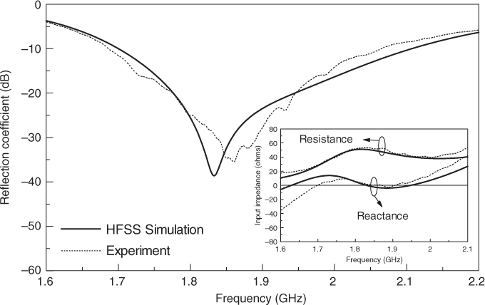
Figure 5.12 Power spectrum shown as a function of frequency for the rectangular solid DRAO in Fig. 5.8. The center frequency is 1.8784 GHz with a span of 50 MHz. (a) Fundamental oscillating signal; (b) fundamental oscillating signal and second harmonic. (From (17), copyright © 2007 IEEE, with permission.)
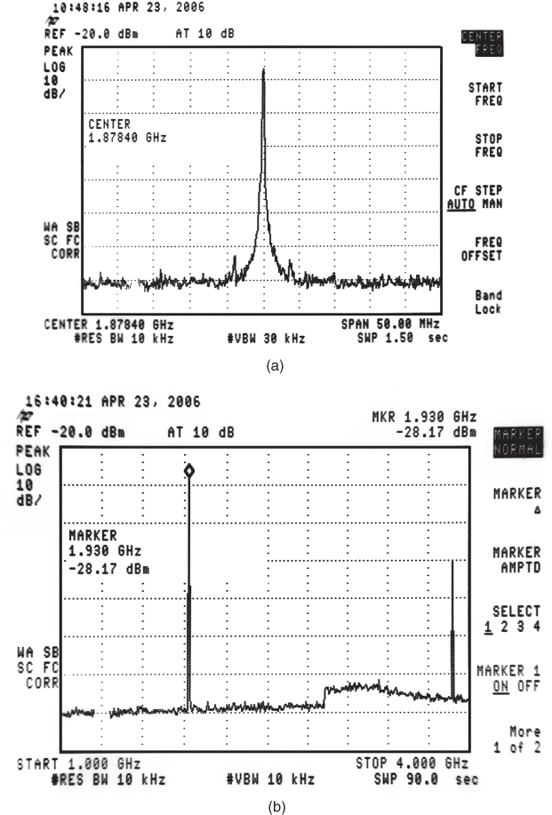
Figure 5.13 Normalized radiation patterns simulated and measured for the rectangular solid DRAO in Fig. 5.8: (a) E-plane (xz-plane). (b) H-plane (yz-plane). The frequencies of the simulated and measured results are 1.83 and 1.878 GHz, respectively. (From (17), copyright © 2007 IEEE, with permission.)
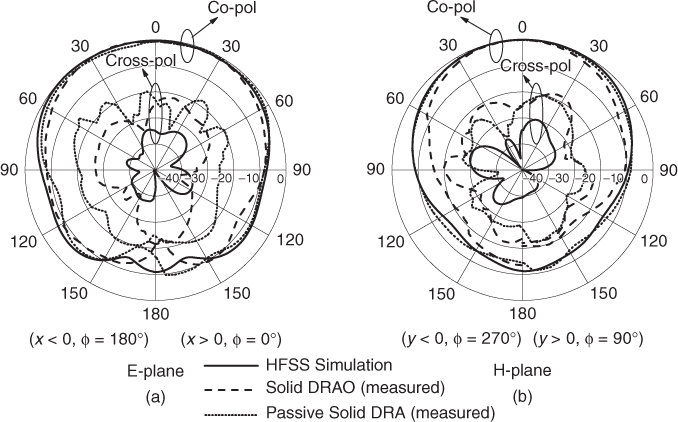
Figure 5.14 Antenna gain measured for the rectangular DRA in Fig. 5.8. (From (17), copyright © 2007 IEEE, with permission.)
5.4.2 Hollow DRAO
5.4.2.1 Configuration
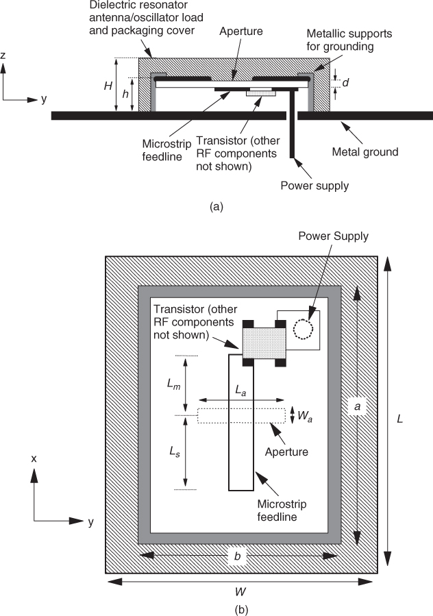
Figure 5.15 shows the configuration of a trifunction hollow DRAO (17). Now, the DR functions simultaneously as an antenna, a packaging cover, and an oscillator load. To design the DRAO, a notched DR is first formed by removing the lower central portion of the solid DR (Fig. 5.8). With the use of the design procedure mentioned in Section 2.4.1, the hollow DRA is then constructed by covering up the two sides which are parallel to the xz-plane of the notched DR. The DRA was designed to resonate fundamentally at 1.85 GHz. The optimized dimensions of the DR were found to be L = 52.2 mm, W = 56.4 mm, H = 26.1 mm, a = 26 mm, b = 42.4 mm, and h = 9 mm. As can be seen in Fig. 5.15, the inner surface of the DR has a conducting coating to isolate the DR from the active circuits placed inside the hollow region. The ground plane of the substrate and the four metallic supports form a rectangular metallic cavity. On top of the substrate, a microstrip-fed aperture of La = 0.434λe, Wa = 2 mm was used to excite the DRA. A shorter interconnecting stub with a length of Lm = 10 mm was used. The length of the matching stub is given by Ls = 7.5 mm. In an experiment a hole was drilled in the ground plane to supply dc bias to the oscillator circuit. An aluminum ground plane of 30 (x-direction) × 20 cm (y-direction) in size was used in the experiment. Since the computer memory is limited, a smaller ground plane of 20 × 20 cm was used in HFSS simulations. The same oscillator (as the rectangular solid DRAO) and HiK powder ( ε r = 6) were used to construct the hollow DRAO.
Figure 5.15 Rectangular hollow DRAO excited by a microstripline-feed aperture: (a) front view; (b) top view. (From (17), copyright © 2007 IEEE, with permission.)
5.4.2.2 Results and Discussion
Figure 5.16 shows the reflection coefficients simulated and measured for the passive hollow DRA (Fig. 5.15), where reasonable agreement is observed. The corresponding input impedances are also shown in the inset. The impedance bandwidth measured (|S11| < − 10 dB) is 5.11%. With reference to the figure, the resonance frequencies measured and simulated are 1.853 and 1.838 GHz, respectively, with an error of 0.816%. Again, with the use of the experimental setup in Fig. 5.9, the power spectrum measured for the trifunction hollow DRAO is illustrated in Fig. 5.17. A stable oscillating frequency of about 1.90 GHz with a clean spectrum is observed. With reference to the figure, the power received, Pr = − 26.5 dBm, was measured at the horn by a spectrum analyzer, which gives an estimated transmitting power of Pt = 17.2 dBm by referring to Fig. 5.10. The dc–RF conversion efficiency is about 15.6%. As can be seen from Fig. 5.17(b), it is noted that the second harmonic is 21.59 dB lower than its fundamental oscillating signal. Comparing with the rectangular solid DRAO, the hollow DRAO in this case has a much better phase noise of −101.5 dBc/Hz at 100 kHz offset because it has a higher loaded Q factor. It has been studied that the Q factor of a microstrip antenna oscillator can be increased by loading an external rectangular metallic cavity on the reverse side of the antenna (18, 19). Obviously, the hollow DRAO in Fig. 5.15 has a much more compact size since the metallic cavity is embedded inside the DRA, wasting no extra space. This compact microwave structure provides a possible solution for the IC packaging. Using the measurement setup in Fig. 5.9, the normalized radiation patterns simulated and measured for the passive DRA and active DRAO are shown in Fig. 5.18. Again, the cross-polarized fields are generally 20 dB weaker than their co-polarized counterparts in both E- (xz-plane) and H-plane (yz-plane). As can be seen from Fig. 5.19, the measured antenna gain fluctuates in the range 3 to 6 dBi in the antenna passband.
Figure 5.16 Reflection coefficients simulated and measured for the rectangular hollow DRA in Fig. 5.15. The inset shows the input impedances simulated and measured as a function of frequency. (From (17), copyright © 2007 IEEE, with permission.)
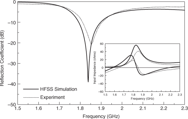
Figure 5.17 Power spectrum as a function of frequency for the hollow DRAO in Fig. 5.15. The center frequency is 1.899555 GHz with a span of 1 MHz. (a) Fundamental oscillating signal; (b) fundamental oscillating signal and second harmonic. (From (17), copyright © 2007 IEEE, with permission.)
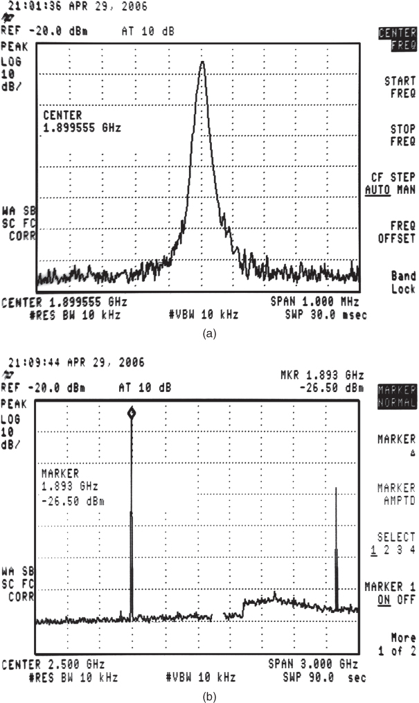
Figure 5.18 Normalized radiation patterns simulated and measured for the rectangular hollow DRAO in Fig. 5.15: (a) E-plane (xz-plane); (b) H-plane (yz-plane). The frequencies of the simulated and measured results are 1.838 and 1.90 GHz, respectively. (From (17), copyright © 2007 IEEE, with permission.)
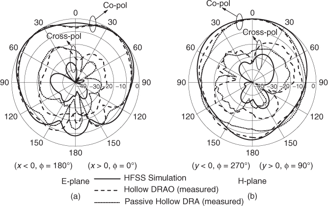
Figure 5.19 Antenna gain measured for the hollow DRA in Fig. 5.15. (From (17), copyright © 2007 IEEE, with permission.)
5.4.3 Differential Planar Antenna Oscillator
5.4.3.1 Configuration
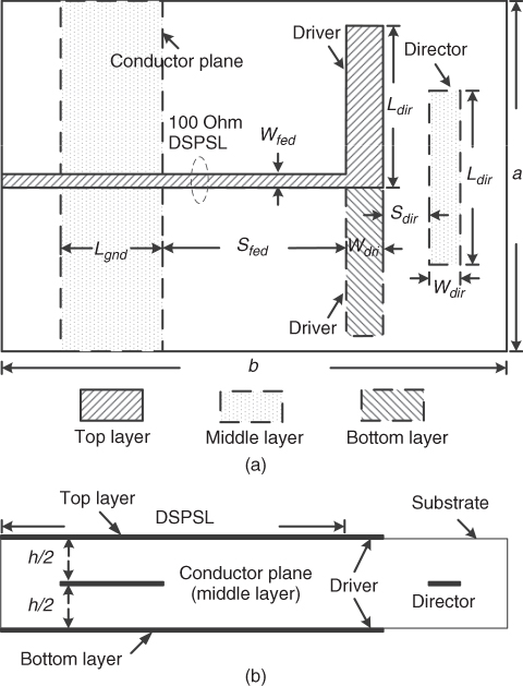
Figure 5.20 shows the configuration of a differential antenna oscillator (23). Here, a quasi-Yagi antenna is used as the oscillator load of a voltage-controlled integrated antenna oscillator (VCIAO). The antenna part of the VCIAO is discussed first. The top and side views of the quasi-Yagi–Uda antenna are shown in Fig. 5.21. The antenna is made on a three-layer substrate with dielectric constant ε r = 3.48 and thickness h = 1.016 mm. As can be seen from the figure, the middle layer contains a director and an inserted conductor plane. The conductive middle layer is also a virtual ground plane and a reflector of the antenna. A feeding 100-Ω double-sided parallel-strip line (DSPSL) (with a linewidth of Wfed) is made up of the metallic lines on the top and bottom layers. As the DSPSL itself is a good balanced transmission line, the signals on the top and bottom lines are constantly frequency independent out-of-phase. It eliminates the need of any additional balun for feeding the antenna. The optimized design parameters of the quasi-Yagi are given by Wfed = 1.26 mm, Lgnd = 14 mm, Ldri = 28.63 mm, Ldir = 35 mm, Sfed = 21.5 mm, Sdir = 5.1 mm, Wdri = Wdir = 5 mm, a = 65 mm, and b = 70 mm.
Figure 5.20 Schematic of a differential quasi-Yagi antenna oscillator. (Courtesy of J. Shi, J. X. Chen, and Q. Xue, City University of Hong Kong. From (23), copyright © 2007 IEEE, with permission.)
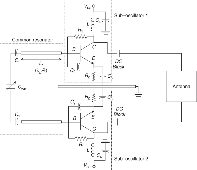
Figure 5.21 Layout of a DSPSL-fed quasi-Yagi antenna: (a) top view; (b) side view. (Courtesy of J. Shi, J. X. Chen, and Q. Xue, City University of Hong Kong. From (23), copyright © 2007 IEEE, with permission.)
HFSS was used to simulate the antenna part of the VCIAO. The reflection coefficient simulated for the passive antenna (shown in Fig. 5.21) is shown in Fig. 5.22. As can be seen from the figure, the impedance bandwidth simulated (|S11| < − 10 dB) is 34%. With reference to the inset, the input resistance is in the range 90 ± 10 Ω and the reactance is in the range 0 ± 15 Ω. The gain is 5.5 to 6.5 dBi across the entire passband in the frequency range 2.2 to 2.8 GHz. The radiation patterns simulated at 2.7 GHz are shown in Fig. 5.23. In both the E- and H-planes, the radiation patterns are broad-side, with a front-to-back ratio better than 17 dB.
Figure 5.22 Reflection coefficient simulated for the passive quasi-Yagi antenna in Fig. 5.21. The inset shows the input impedance simulated as a function of frequency. (Courtesy of J. Shi, J. X. Chen, and Q. Xue, City University of Hong Kong. From (23), copyright © 2007 IEEE, with permission.)
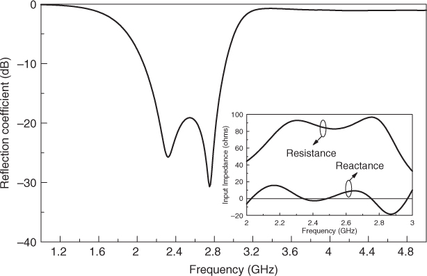
Figure 5.23 Radiation patterns simulated for the passive quasi-Yagi antenna in Fig. 5.21. (a) E-plane; (b) H-plane. (Courtesy of J. Shi, J. X. Chen, and Q. Xue, City University of Hong Kong. From (23), copyright © 2007 IEEE, with permission.)
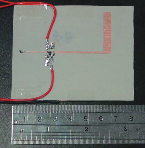
Next, a differential voltage-controlled integrated antenna oscillator (VCIAO) is constructed by inserting a pair of Infineon BFP650 transistors onto the top and bottom layers, right above and below the inserted conductor planes, of the substrate. The configuration is shown in Fig. 5.24. For brevity, the biasing and feedback circuits (dc voltage supply Vcc, capacitors C2 to C4, resistors R1 to R2, and inductor L in Fig. 5.20) are not shown. The middle-layer conductor plane serves as the ground for the differential VCO as well as the reflector for the antenna. As can be seen from Fig. 5.24(c), a DSPSL-fed quasi-Yagi antenna is built on the right-hand side of the inserted ground plane while a quarter-wavelength resonator is built on the left-hand side. A varactor was embedded in a perforation penetrating the substrate, and it was connected to the λg/4 resonator going through a capacitor C1. Obviously, the differential VCO is composed by two identical suboscillators being placed on the two opposite surfaces of the substrate. The design parameters of the VCIAO are as follows: Lr = 15.8 mm, Wr = 0.5 mm, a = 65 mm, b = 80 mm, and the dimension of the antenna is identical to that of the passive case (Fig. 5.21). The chip capacitor C1 is 1 pF and the varactor diode is Skyworks' SMV1247-079LF. Both transistors are biased at VCE = 3.5 V with a total current of IC = 41 mA. A fabricated VCIAO is shown in Fig. 5.25.
Figure 5.24 Configuration of a VCIAO: (a) three-dimensional view; (b) side view; (c) top view. (Courtesy of J. Shi, J. X. Chen, and Q. Xue, City University of Hong Kong. From (23), copyright © 2007 IEEE, with permission.)
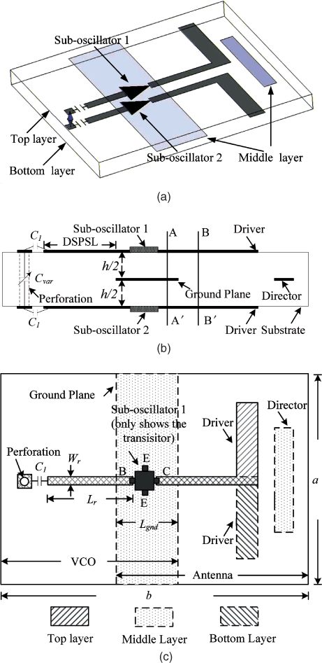
Figure 5.25 Top view of the VCIAO in Fig. 5.24. (Courtesy of J. Shi, J. X. Chen, and Q. Xue, City University of Hong Kong. From 5 (23), copyright © 2007 IEEE, with permission.)
As mentioned by Shi et al. (23), the co-design procedure of the VCIAO can be summarized as follows:
5.4.3.2 Measurement Method
The transmitting power from the VCIAO is measured using the active antenna test range setup (1) in an anechoic chamber. Use is made of the Friis transmission equation for calculating the radiated power of the antenna oscillator. The measurement setup is shown in Fig. 5.26. Different from the measurement setup in Section 5.4.1, here the radiated power (Pr) of the active transmitting antenna is directly illuminated on the receiving reference horn. A short coaxial cable (cable loss of Lcable = − 2 dB) is used to connect the double-ridged horn antenna (antenna gain Gr = 8.3 dBi) to the HP 8593E spectrum analyzer for measuring the received power. The separation distance is D = 4 m, being in the far field. The effective isotropic radiated power (EIRP) can be calculated using (5.10). The information of the transmitting antenna gain (Gt) is included by EIRP.
When the varactor is biased at 2.7 V, the radiated power is found to be Pr = − 25.6 dBm at 2.69 GHz (shown in Fig. 5.27). It can easily be calculated from (5.10) that the corresponding EIRP is 21.2 dBm.
Figure 5.26 Active antenna test range setup.
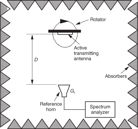
Figure 5.27 Output power spectrum received at a frequency of 2.69 GHz for the VCIAO in Fig. 5.24. (Courtesy of J. Shi, J. X. Chen, and Q. Xue, City University of Hong Kong. From (23), copyright © 2007 IEEE, with permission.)
5.4.3.3 Results and Discussion
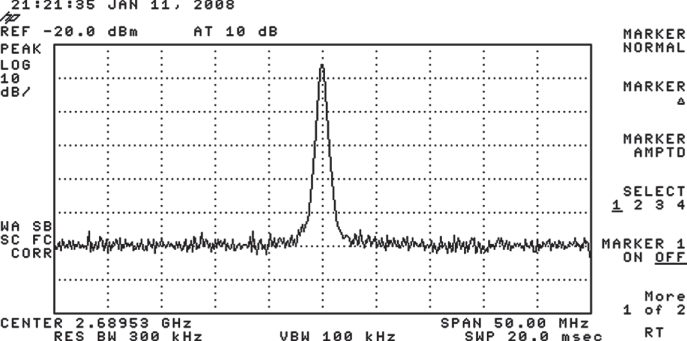
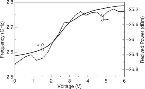
In Fig. 5.28, the phase noise of the VCIAO at the oscillation frequency of 2.69 GHz is shown. With reference to the figure, the phase noise reads about −92 dBc/Hz at 100 kHz offset and −112 dBc/Hz at 500 kHz offset. As can be seen from Fig. 5.29, the tuning range of the VCIAO is 2.585 to 2.785 GHz, with about 1.4 dB of amplitude variation. From the figure it can be observed that the antenna oscillator has a gain of 66.7 MHz/V in the linear tunable range 2.61 to 2.73 GHz.
Figure 5.28 Phase noise measured for the VCIAO in Fig. 5.24. (Courtesy of J. Shi, J. X. Chen, and Q. Xue, City University of Hong Kong. From (23), copyright © 2007 IEEE, with permission.)
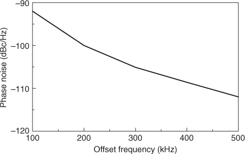
Figure 5.29 Results of the tuning frequency range and received output power measured for the VCIAO in Fig. 5.24. (Courtesy of J. Shi, J. X. Chen, and Q. Xue, City University of Hong Kong. From (23), copyright © 2007 IEEE, with permission.)
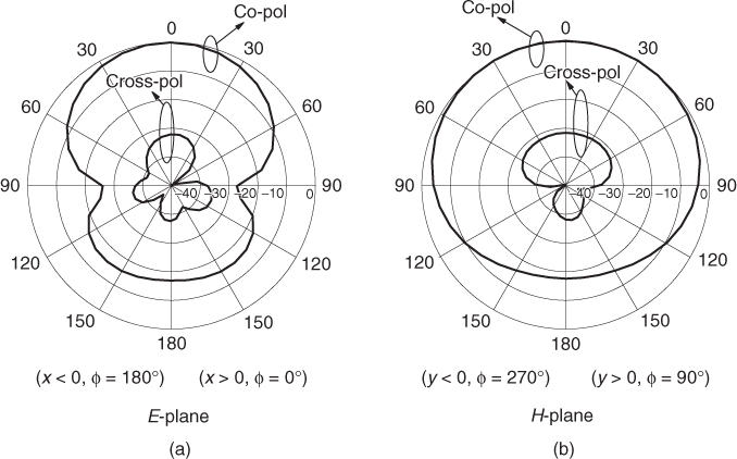
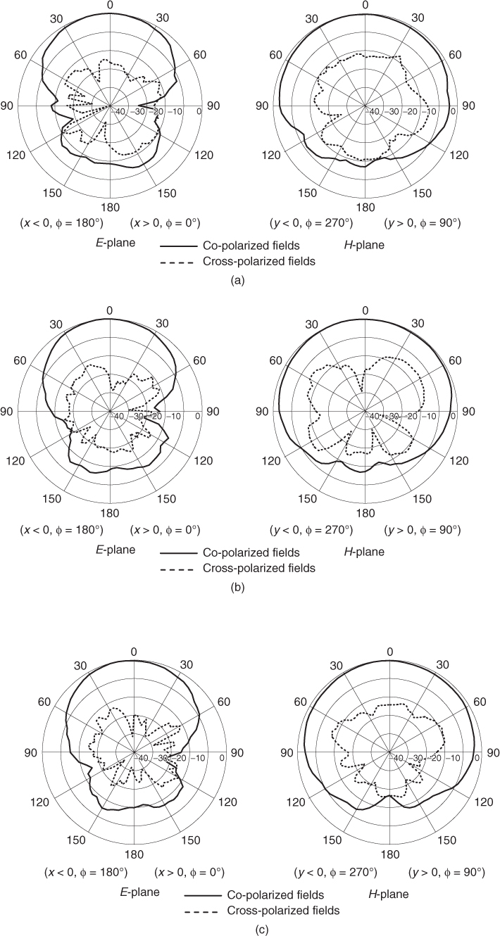
By rotating the rotator, the co- and cross-polarized radiation patterns were measured in the E- and H-planes at oscillation frequencies of 2.61, 2.69, and 2.77 GHz. The results are shown in Fig. 5.30. At all three frequencies, the co-polarized fields are greater than their cross-polarized counterparts by at least 20 dB. This shows that the VCIAO has a good linear polarization. In general, the front-to-back ratio is better than 16 dB.
Figure 5.30 Radiation patterns measured for the VCIAO in Fig. 5.24: (a) 2.62 GHz; (b) 2.69 GHz; (c) 2.76 GHz. (Courtesy of J. Shi, J. X. Chen, and Q. Xue, City University of Hong Kong. From (23), copyright © 2007 IEEE, with permission.)
5.5 Coupled-load Antenna Oscillators
5.5.1 Coupled-Load Microstrip Patch Oscillator
5.5.1.1 Configuration
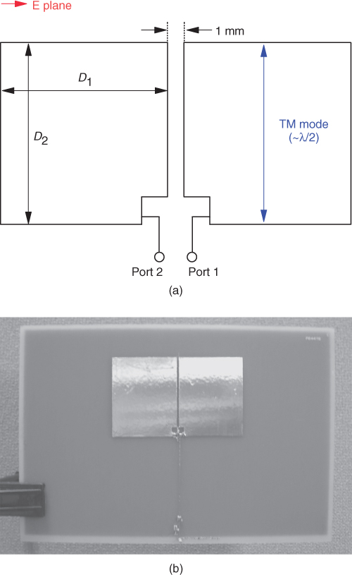
By making an antenna simultaneously the feedback load of an amplifier, the coupled-load antenna oscillator can easily be designed, as noted in Section (24). To demonstrate the design idea, the Mini-Circuits ERA-2SM broadband RF amplifier is integrated with a microstrip dual-patch antenna for the construction of a coupled-load antenna oscillator (25). The schematic of the antenna oscillator is shown in Fig. 5.31, where the numberings represent the chip pinouts. The design parameters are Rb = 100 Ω, Cblock = 1000 pF, RFC = 680 nH, and Vcc = 7.5 V. It is given in the datasheet that the amplifier has a typical gain of about 16 dB at 1 GHz. With reference to Fig. 5.32(a), the antenna is designed from a pair of symmetric rectangular ( ∼ λ/2) patches with corner cutouts for accommodating the amplifier. It is designed on a FR-4 (with a thickness of 62 mils) with dimension D1 = 48.5 mm and D2 = 59 mm. The prototype is shown in Fig. 5.32(b). To ensure stable oscillation, according to the Barkhausen criterion it is imperative that |Hant(jω)Hamp(jω)| = 1 and ∠Hant(jω)Hamp(jω) = 0°. Here Hamp(jω) and Hant(jω) are the transfer functions of the amplifier and antenna, respectively.
Figure 5.31 Schematic of a coupled-load microstrip patch oscillator.
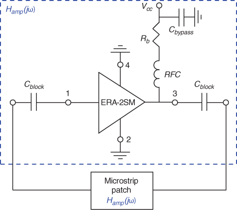
Figure 5.32 (a) Configuration of a microstrip dual-patch antenna; (b) photograph of a microstrip dual-patch antenna. (Courtesy of S. Makarov, Worcester Polytechnic Institute. From (25), copyright © 2005 IEEE, with permission.)
5.5.1.2 Results and Discussion
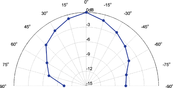
Figure 5.33 shows the simulated open-loop magnitude |Hant(jω)Hamp(jω)| and the simulated open-loop angle ∠Hant(jω)Hamp(jω). Oscillation occurs at around the frequency marked by a diamond-shaped marker. At this frequency, the open-loop angle is 0°. The oscillation frequency is measured by a receiving antenna (gain ∼5 dBi) at a distance of 1 m. With reference to Fig. 5.34, the peak power is about −33 dB, with a center oscillation frequency of 1.261 GHz. The phase noise measured for the antenna oscillator is about −120 dBc/Hz at 1 MHz, as shown in Fig. 5.35. By tuning the Vcc over a range of 6.5 to 8.1 V, the tuning sensitivity measured for the antenna oscillator is found to be about 1.13 MHz/V, as shown in Fig. 5.36. The radiation fields were measured in the E-plane and the result is shown in Fig. 5.37. In general, the co-polarized field is isolated from its cross-polarized counterpart by at least 20 dB.
Figure 5.33 Open-loop magnitude and angle simulated for the antenna oscillator in Fig. 5.31. (Courtesy of S. Makarov, Worcester Polytechnic Institute.)
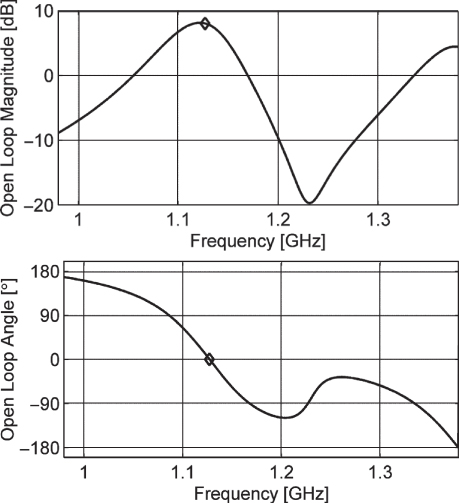
Figure 5.34 Power spectrum as a function of frequency for the microstrip dual-patch antenna oscillator in Fig. 5.31. The center frequency is 1.261 GHz with a span (range of x-axis) of 502.3 kHz. (Courtesy of S. Makarov, Worcester Polytechnic Institute.)
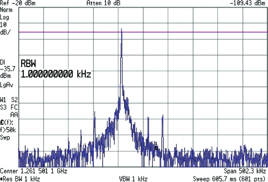
Figure 5.35 Phase noise measured for the microstrip dual-patch antenna oscillator in Fig. 5.31. (Courtesy of S. Makarov, Worcester Polytechnic Institute.)
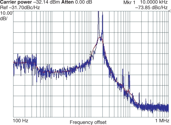
Figure 5.36 Tuning sensitivity measured for the microstrip dual-patch antenna oscillator in Fig. 5.31. (Courtesy of S. Makarov, Worcester Polytechnic Institute. From (25), copyright © 2005 IEEE, with permission.)
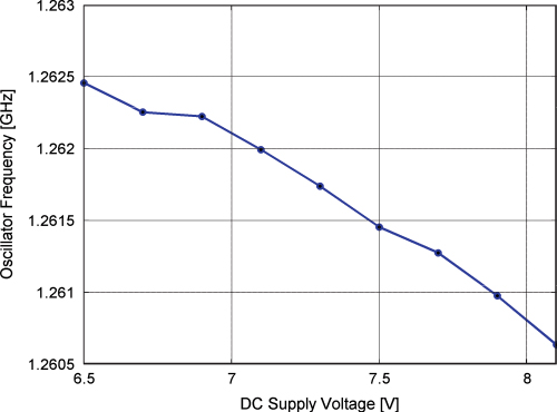
Figure 5.37 Co-polarized pattern measured in the E-plane. (Courtesy of S. Makarov of Worcester Polytechnic Institute. From (25), copyright © 2005 IEEE, with permission.)
5.5.2 Patch Antenna Oscillator with Feedback Loop
5.5.2.1 Configuration
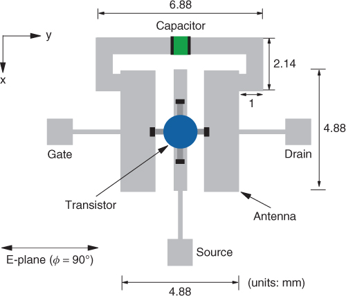
A very compact feedback-type antenna oscillator was designed by Mueller et al. (26) on a high-dielectric-constant microwave substrate ( ε r = 10.2 and thickness-0.635 mm). In this case, a capacitor-loaded microstrip antenna is used as the feedback element of an oscillator. Despite being placed on a high-permittivity substrate, the radiation efficiency of the antenna oscillator remains good, achieving a high radiation power. The configuration of the antenna oscillator is shown in Fig. 5.38. The antenna consists of two patches interconnected by a narrow stripline. A capacitor is inserted into the middle point of the narrow line to construct a feedback loop. The antenna, capacitor, and feedlines have a total electrical length (∠S21antenna) of ![]() , where λg is the guided wavelength. It was found that the antenna has current distribution similar to that for a conventional microstrip patch antenna. To oscillate, the transistor has to provide an additional phase (∠S21transistor) so that ∠S21antenna + S21transistor = 0°. The NEC super-low-noise high-frequency field-effect transistor (HF FET) NE3210S01 is used for the oscillator design (27). This is a pseudomorphic heterojunction field-effect transistor, which has a 0.20-μm gate length and a 160-μm gate width. The transistor was biased using a single 1.5-V battery placed between the source and drain terminals. The gate terminal is left open. The amplifier gain of this transistor is about 8.5 to 9 dB over the frequency range 6 to 12 GHz. A 1.2-pF capacitor was used as the dc isolator between the drain and gate as well as the feedback element of the antenna oscillator. Both the antenna and oscillator are fabricated on a RT/Duroid 6010LM substrate ( ε r = 10.2 and thickness = 0.635 mm). The antenna oscillator is designed to operate at 8.50 GHz, occupying an area of 5 × 6 mm2. The active integrated antenna shows stable oscillation and an excellent radiation pattern across the entire X band.
, where λg is the guided wavelength. It was found that the antenna has current distribution similar to that for a conventional microstrip patch antenna. To oscillate, the transistor has to provide an additional phase (∠S21transistor) so that ∠S21antenna + S21transistor = 0°. The NEC super-low-noise high-frequency field-effect transistor (HF FET) NE3210S01 is used for the oscillator design (27). This is a pseudomorphic heterojunction field-effect transistor, which has a 0.20-μm gate length and a 160-μm gate width. The transistor was biased using a single 1.5-V battery placed between the source and drain terminals. The gate terminal is left open. The amplifier gain of this transistor is about 8.5 to 9 dB over the frequency range 6 to 12 GHz. A 1.2-pF capacitor was used as the dc isolator between the drain and gate as well as the feedback element of the antenna oscillator. Both the antenna and oscillator are fabricated on a RT/Duroid 6010LM substrate ( ε r = 10.2 and thickness = 0.635 mm). The antenna oscillator is designed to operate at 8.50 GHz, occupying an area of 5 × 6 mm2. The active integrated antenna shows stable oscillation and an excellent radiation pattern across the entire X band.
Figure 5.38 Configuration of an antenna oscillator with a capacitor-loaded feedback patch antenna.
5.5.2.2 Results and Discussion
A calibrated Agilent E8361A PNA and an Agilent 4448A spectrum analyzer were used to measure the S parameters and power spectrums, respectively. The radiation measurements were performed in a far-field anechoic chamber located at the NASA–Glenn Research Center (Cleveland, OH). A standard horn antenna (Gr = 10 dBi at 8.5 GHz) was used. By connecting the horn to the spectrum analyzer, the power radiated was measured at a distance of 135 cm. For a characterization of the radiation patterns, an HP 437 power meter was used to measure the received powers of the co- and cross-polarized fields, with the horn placed at a distance of 665 cm. In this case, a stepping-motor-driven rotational stage, rotating with an 0.25° increment, was employed.
The frequency discriminator method (28) was adopted to measure phase noise. An Agilent E5500 phase noise measurement system was used. The measurement procedure is described briefly here. The received signal is first split into two paths. A coaxial delay line (35 ns) is inserted into one of the signal paths so that the noise between the two paths is uncorrelated at the offset frequency. The delay line also acts as a frequency-to-phase transformer. Then an amplifier is placed in the same path to compensate the insertion loss of the delay line. A manually tunable phase shifter (HP X885 A) is connected to another signal path so that the signals in the two paths are at quadrature. Finally, the Agilent E5500 is used as a mixer, and the phase noise is measured using an Agilent 4411 B ESA-L series spectrum analyzer. To determine the phase detector constant, an Agilent E8257C PSG analog signal generator is used to perform the double-sided spur calibration.
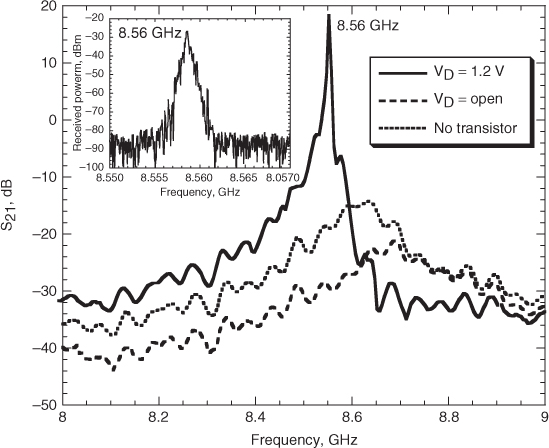
The test fixture in Fig. 5.39 is deployed to measure concurrently the S parameters and radiated power of the antenna oscillator in an anechoic chamber. The transistor drain (port 1) and gate (port 2) terminals are wire-bonded to two microstrips of the test fixture for connection to a calibrated Agilent E8361A PNA with an input power of −15 dBm. Transmission coefficient (S21) is then taken for three settings: (1) with the transistor removed, (2) with the transistor mounted but no bias (VD = open) applied, and (3) with the transistor mounted and biased (VD = 1.2 V, with the source grounded and the gate opened). The transmission coefficients measured are shown in Fig. 5.40. As can be seen from the figure, there is a peak observed at 8.65 GHz, with a QL value of about 70. With the transistor biased, oscillation occurs as ∠S21antenna + S21transistor = 0°. In this case, the transmission coefficient is about 19 dB at 8.56 GHz. The inset of Fig. 5.40 shows the concurrently measured radiation power of the antenna oscillator. It shows clearly that the device radiates at the frequency where S21 is maximum.
Figure 5.39 Antenna oscillator with a capacitor-loaded feedback patch antenna. (Courtesy of F. A. Miranda, NASA–Glenn Research Center, Cleveland, Ohio. From (26), copyright © 2008 IEEE, with permission.)
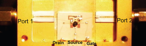
Figure 5.40 Transmission (S21) versus frequency for the antenna oscillator under three different settings. The inset shows the measured radiated power, with the detector located 37 cm from the antenna oscillator. (Courtesy of F. A. Miranda, NASA–Glenn Research Center, Cleveland, Ohio. From (26), copyright © 2008 IEEE, with permission.)
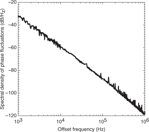
Next, the antenna oscillator is unsoldered from the test fixture. To measure the radiation pattern, it is remounted on a 3.0 × 3.0 cm flat metal plate. The transistor is biased at Vg = open, Vd = 1.5 V, and Id = 17.7 mA. Figures 5.41 and 5.42 show the power spectrum received and the phase noise measured, respectively. At 100 kHz offset, the antenna oscillator has a phase noise of −87.5 dBc/Hz, which is quite high, as the Q factor for the antenna is usually low.
Figure 5.41 Power radiated from the antenna oscillator in Fig. 5.38, with the detector located 132 cm away (resolution bandwidth = video bandwidth = 47 kHz). (Courtesy of F. A. Miranda, NASA–Glenn Research Center, Cleveland, Ohio. From (26), copyright © 2008 IEEE, with permission.)
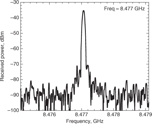
Figure 5.42 Phase noise measured for the antenna oscillator (VDS = 1.5 V) in Fig. 5.38. (Courtesy of F. A. Miranda, NASA–Glenn Research Center, Cleveland, Ohio. From (26), copyright © 2008 IEEE, with permission.)
At the receiving horn, the EIRP of the antenna oscillator can be calculated by EIRP = PtDt = Pr/Gr(λo/4πR), where Pt is the transmitted power and Dt is the directivity of the antenna oscillator [29]. Pr ( = − 46.3 dBm) is the power received by the horn (Gr), λo ( = 3.54 cm at 8.48 GHz) is the free-space wavelength, and R ( = 665 cm) is the distance between the two antennas. The EIRP of the antenna oscillator is then calculated as 11.2 dBm. Assuming that the antenna is unidirectional and the directivity can be estimated by Dt = 41, 253/θ1ϕ1 = 6.74 dB (30), the radiated power Pt is calculated as 4.72 dBm. θ1 ( = 72°) and ϕ1 ( = 85°) are the 3-dB beamwidths in the E- and H-planes, respectively. This corresponds to a dc-to-RF conversion efficiency of 10.5%.
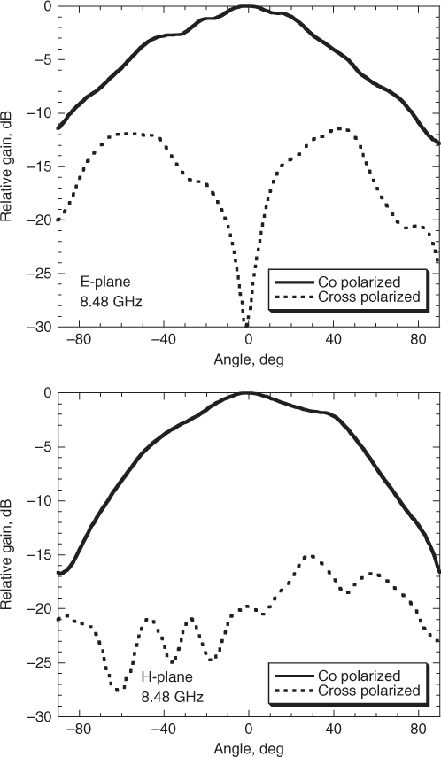
Figure 5.43 shows the radiation patterns measured in the E- and H-planes. The co-polarized fields are at least 20 dB larger than their cross-polarized counterparts in both planes, indicating good linear polarization. Low cross-polarization can be caused by the small circuit size.
Figure 5.43 Normalized radiation measured for the capacitor-load feedback patch antenna in Fig. 5.38. (Courtesy of F. A. Miranda, NASA-Glenn Research Center, Cleveland, Ohio. From (26), copyright © 2008 IEEE, with permission.)
5.6 Conclusions
Recent developments of the reflection-amplifier and coupled-load antenna oscillators have been covered in this chapter. The design methodologies and measurement procedures of the two types of active antennas are discussed, along with several design examples. Despite its various advantages, the performance of the antenna oscillators is limited by the antenna Q factor, which is usually low. Techniques on improving the Q factor have been elaborated. Several successful practical designs of antenna oscillators have also been demonstrated. Finally, some contemporary design issues have been highlighted. With the advent of millimeter-wave and teraheltz eras, antenna oscillators may possibly be used for spatial power combining and other applications.
References
1. J. A. Navarro and K. Chang, Integrated Active Antennas and Spatial Power Combining. New York: Wiley, 1996.
2. K. Chang, I. Bahl, and V. Nair, RF and Microwave Circuit and Component Design for Wireless Systems. Hoboken, NJ: Wiley, 2002.
3. A. Mortazawi, T. Itoh, and J. Harvey, Active Antennas and Quasi-optical Arrays. Piscataway, NJ: IEEE Press, 1998.
4. G. D. Vendelin, A. M. Pavio, and U. L. Rohde, Microwave Circuit Design: Using Linear and Nonlinear Techniques. Hoboken, NJ: Wiley, 2005.
5. S. A. Maas, Nonlinear Microwave and RF Circuits, 2nd ed. Boston: Artech House, 2003.
6. G. Gonzalez, Microwave Transistor Amplifier: Analysis and Design, 2nd ed. Englewood Cliffs, NJ: Prentice Hall, 1984.
7. K. Kurokawa, Some basic characteristics of broadband negative resistance oscillator circuits, Bell Sys. Tech. J., vol. 48, pp. 1937–1955, 1969.
8. E. N. Ivanov and M. E. Tobar, Low phase-noise microwave oscillators with interferometric signal processing, IEEE Trans. Microwave Theory Tech., vol. 54, pp. 3284–3294, Aug. 2006.
9. L. Zhou, Z. Wu, M. Sallin, and J. Everald, Broad tuning ultra low phase noise dielectric resonator oscillators using SiGe amplifier and ceramic-based resonators, IET Microwave Antennas Propag., vol. 1, no. 5, pp. 1064–1070, Oct. 2007.
10. Q. Xue, K. M. Shum, and C. H. Chan, Novel oscillator incorporating a compact microstrip resonant cell, IEEE Microwave Wireless Compon. Lett., vol. 11, pp. 202–204, May 2001.
11. K. Kawasaki, T. Tanaka, and M. Aikawa, An octa-push oscillator at V-band, IEEE Trans. Microwave Theory Tech., vol. 58, pp. 1696–1702, July 2010.
12. S. L. Jang, C. C. Liu, C. Y. Wu, and M. H. Juang, A 5.6GHz low power balanced VCO in 0.18μm CMOS, IEEE Microwave Wireless Compon. Lett., vol. 19, pp. 233–235, Apr. 2009.
13. P. Ruippo, T. A. Lehtonen, and N. T. Juang, An UMTS and GSM low phase noise inductively tuned LC VCO, IEEE Microwave Wireless Compon. Lett., vol. 20, pp. 163–165, Mar. 2010.
14. F. Giuppi, A. Georgiadis, A. Collado, M. Bozzi, and L. Perregrini, Tunable SIW cavity backed active antenna oscillator, Electron. Lett., vol. 46, no. 15, pp. 1053–1055, July 2010.
15. C. H. Mueller, R. Q. Lee, R. R. Romansofsky, C. L. Kory, K. M. Lambert, F. W. V. Keuls, and F. A. Miranda, Small-size X-band active integrated antenna with feedback loop, IEEE Trans. Antennas Propag., vol. 56, pp. 1236–1241, May 2008.
16. O. Y. Buslov, A. A. Golovkov, V. N. Keis, A. B. Kozyrev, S. V. Krasilnikov, T. B. Samoilova, A. Y. Shimko, D. S. Ginley, and T. Kaydanova, Active integrated antenna based on planar dielectric resonator with tuning ferroelectric varactor, IEEE Trans. Microwave Theory Tech., vol. 55, pp. 2951–2956, Dec. 2007.
17. E. H. Lim and K. W. Leung, Novel utilization of the dielectric resonator antenna as an oscillator load, IEEE Trans. Antennas Propag., vol. 55, pp. 2686–2691, Oct. 2007.
18. M. Zheng, Q. Chen, P. S. Hall, and V. F. Fusco, Oscillator noise reduction in cavity-backed active microstrip patch antenna, Electron. Lett., vol. 33, no. 15, pp. 1276–1277, July 1997.
19. M. Zheng, P. Gardener, P. S. Hall, Y. Hao, Q. Chen, and V. F. Fusco, Cavity control of active integrated antenna oscillators, Microwave Antennas Propag., vol. 148, no. 1, pp. 15–20, Feb. 2001.
20. Y. Chen and Z. Chen, A dual-gate FET subharmonic injection-locked self-oscillating active integrated antenna for RF transmission, IEEE Microwave Wireless Compon. Lett., vol. 13, pp. 199–201, June 2003.
21. R. K. Mongia and A. Ittipiboon, Theoretical and experimental investigations on rectangular dielectric resonator antennas, IEEE Trans. Antennas Propag., vol. 45, pp. 1348–1356, Sept. 1997.
22. HP85301CK02 Antenna Measurement System: Operating and Service Manual Supplement.
23. J. Shi, J. X. Chen, and Q. Xue, A differential voltage-controlled integrated antenna oscillator based on double-sided parallel-strip line, IEEE Trans. Antennas Propag., vol. 56, pp. 2207–2212, Oct. 2008.
24. K. Chang, K. A. Hummer, and G. K. Gopalakrishnan, Active radiating element using FET source integrated with microstrip patch antenna, Electron. Lett., vol. 24, no. 21, pp. 1347–1348, Oct. 1988.
25. I. Waldron, A. Ahmed, and S. Makarov, Amplifier-Based Active Antenna Oscillator Design at 0.9–1.8 GHz, IEEE/ACES International Conference on Wireless Communications and Applied Computational Electromagnetics, Honolulu, HI, Apr. 3–7. 2005, pp. 775–778.
26. C. H. Mueller, R. Q. Lee, R. R. Romanofsky, C. L. Kory, K. M. Lambert, F. W. Van Keuls, and F. A. Miranda, Small-size X-band active integrated antenna with feedback loop, IEEE Trans. Antennas Propag., vol. 56, pp. 2686–2691, May 2008.
27. http://www.cel.com/pdf/datasheets/NE3210S01.pdf.
28. Hewlett Packard Product Note 11729C-3, A User's Guide for Automatic Phase Noise Measurements, 1986.
29. C. A. Balanis, Antenna Theory Analysis and Design, 2nd ed. New York: Wiley, 1997.
30. W. L. Stutzman and G. A. Thiele, Antenna Theory and Design, 2nd ed. New York: Wiley, 1998.