
4
Connecting High-Speed Devices Using Buses and Interconnects
This chapter begins by giving an overview of the buses and interconnects used off-chip to connect an FPGA-based SoC to other high-speed devices on the electronics board. It introduces the PCIe interconnect, the Ethernet interconnect, and the emerging Gen-Z protocol. It also provides a good overview of the emerging CCIX interconnect protocol and the concept of extending data coherency off-chip by adding protocol layers in the SoC hardware to implement it.
In this chapter, we’re going to cover the following main topics:
- An overview of the legacy off-chip interconnects
- An introduction to the PCIe bus
- An overview of the Ethernet interconnects
- An introduction to the Gen-Z bus protocol
- An overview of the CCIX protocol and off-chip data coherency
Legacy off-chip interconnects overview
Connecting devices together using off-chip buses and interfaces is necessary to construct an electronics system made up of many integrated circuits (ICs). The need to use these buses is to satisfy the requirements of these ICs to exchange data as they collaborate to implement a more complex function in comparison to what they can achieve on their own. The electronics industry has seen the emergence of many standards and protocols to address this need, and the choice of using a specific protocol depends on many factors, such as the physical IO standards, the speed that these buses can run at, the implementation cost, the versatility of the protocol in the industry, the throughput that they can provide, and so on. We distinguish between two main categories of buses in legacy and modern systems: the protocols suited to carry control data and signaling between devices, and the buses that carry high-throughput payload data at a relatively high speed. The legacy buses have several standards and protocols in use, such as the Serial Peripheral Interface (SPI), the Inter-Integrated Circuit (IIC, but also known as I2C), the Universal Asynchronous Receiver-Transmitter (UART) interface, and many custom buses implemented using a serial or parallel custom protocol carried over low-speed General Purpose Input/Output (GPIO) interfaces. In this section, we will briefly introduce the SPI and I2C buses as some of the most common legacy bus protocols; for a more in-depth study of these bus standards, you are encouraged to examine the respective bus standard specification referenced in their respective section that follows.
SPI overview
The SPI is a simple serial synchronous bus protocol developed by Motorola in the 1980s for connecting a master and a slave device. It is implemented using four signals:
- SCLK: Serial clock, a signal generated by the master
- MOSI: Master out slave in, an output data signal from the master
- MISO: Master in slave out, an output data signal from the slave
- SS: Slave select, an output control signal from the master to a specific slave device, acting as a chip select (CS) signal
The following diagram illustrates the connectivity between a master and a slave SPI device:

Figure 4.1 – SPI bus connecting a master and a slave SPI device
Information
Further information regarding the SPI bus protocol is available in the SPI specification, which can be accessed at https://www.nxp.com/files-static/microcontrollers/doc/ref_manual/S12SPIV4.pdf.
When included in an SoC as an external bus interface, it is integrated into the design within a controller that also provides an internal interface usually via the ARM AMBA APB bus connecting it to the SoC. The SPI controller provides a register file via which the SoC CPU can configure the SPI bus operation modes and speeds. The SPI controller usually supports the full-duplex operation by performing simultaneous receives and transmits. It can buffer the read and write operations within a transmit and a receive FIFO. The master clock frequencies are programmable to adapt to the SoC and external device operational needs. The SoC CPU can control the SPI controller through polling or can use interrupts.
Zynq-7000 SoC SPI controller overview
The following diagram provides a micro-architectural view of the APB SPI controller included in the Xilinx Zynq-7000 SoC processor subsystem (PS) block:

Figure 4.2 – Example SPI controller – the Zynq-7000 SoC
The Xilinx SPI controller can operate either in master or slave mode. In the master mode, the SPI controller can write data out to the slave over the SPI bus or trigger a read operation from the slave. It can interface with up to three slave SPI devices and can distinguish among them using one of the three SS signals (SS[2:0]). Both the SCLK and MOSI are controlled by the master. To write the data from the master to the slave, the SoC CPU writes it first into the transmit FIFO over the APB interface, the SPI controller hardware, then serializes the data out on the MOSI pin. The data write operation is continuous while there is still data in the transmit FIFO of the SPI controller. The read data is received serially via the MISO pin and written by the SPI controller hardware 8 bits at a time into the receive FIFO of the SPI controller. The SCLK frequency can reach 50 MHz in the Zynq-7000 SoC FPGAs, giving a decent data bandwidth for a low-throughput interface.
Information
For further operational and configuration details of the Zynq-7000 SoC SPI controller, you are encouraged to examine section 17 of the Zynq-7000 SoC Technical Reference Manual, which can be found at https://docs.xilinx.com/v/u/en-US/ug585-Zynq-7000-TRM.
I2C overview
I2C was invented by Philips in the 1980s; it is also a serial bus protocol using packet switching as a data transport mechanism between the electronics systems’ components. It only requires two bidirectional signals:
The following diagram illustrates the connectivity between a controller and a target device:

Figure 4.3 – I2C bus connecting a controller and target devices
Every device on the I2C bus is assigned a unique address by the system software. Controllers can operate as transmitters or receivers. The I2C bus protocol allows system topologies to include many controllers on the bus, as it has collision detection and arbitration capabilities that help in preventing data transmission errors if multiple controllers start transmitting at the same time. Data transfer is 8-bit oriented and the throughput in the bidirectional case can achieve up to the following:
- 100 KB in Standard mode
- 400 KB in Fast mode
- 1 MB in Fast-mode Plus
- 3.4 MB in High-speed mode
In the 8-bit oriented unidirectional case, the data transfer throughput can reach up to 5 MB in Ultra-Fast mode.
The maximum bus capacitance (400 pF) and the 7-bit (or in extended mode 10-bit) address space are the only limitations to the number of ICs that can be interconnected using the same I2C bus.
Information
For an in-depth study of the I2C bus standard, you are encouraged to examine its specification available from NXP at https://www.nxp.com/webapp/Download?colCode=UM10204.
When used in an SoC as an external bus interface, the I2C controller usually uses an SoC bus interface such as the APB to connect to the SoC interconnect. The I2C controller provides a register file via which the SoC CPU can configure the I2C bus operation modes and speeds that the I2C controller supports. The master clock frequencies are programmable to adapt to the SoC and external device operation’s needs. The SoC CPU can control the I2C controller through polling or can use interrupts.
Zynq-7000 SoC I2C controller overview
The following diagram provides a micro-architectural view of the APB I2C controller included in the Zynq-7000 SoC PS block:

Figure 4.4 – Example I2C controller – the Zynq-7000 SoC
The Xilinx I2C controller can operate either in master or slave mode. In the master mode, the I2C controller can write data out to the slave over the I2C bus or request a read operation from the slave. The Xilinx Zynq-7000 SoC I2C controller supports only the Standard mode (100 KB) and the Fast mode (400 KB) transfer modes.
Information
For in-depth operational and configuration details of the Zynq-7000 SoC I2C controller, you are encouraged to examine section 20 of the Zynq-7000 SoC Technical Reference Manual, which can be found at https://docs.xilinx.com/v/u/en-US/ug585-Zynq-7000-TRM.
Introduction to the PCIe interconnect
The Peripheral Component Interface Express (PCIe) is a high-speed, multi-layer, and serial interconnect protocol. Its predecessor, the Peripheral Component Interface eXtended (PCI-X), was a parallel interface, but most of its base architectural properties are included in PCIe. The PCIe protocol defines three protocol layers: the transaction layer, the data link layer, and the physical layer. The physical layer uses multi-gigabit transceivers and can communicate at tens of gigabits per second. The physical layer topology is formed of multiple parallel transceivers known as lanes to transport data at a high bandwidth to match the application data transfer rates requirement. There are now many generations of PCIe protocol and all are backward compatible, from generation 1 (Gen1) to generation 6 (Gen6).
Historical overview of the PCIe interconnect
The first PCIe generation, Gen1, was introduced in 2003 as a replacement for the PCI-X parallel interconnect; since then, each subsequent generation was introduced after a few years to basically double the throughput of its predecessor and add features deemed necessary by system applications where PCIe was or can potentially be used. The following table summarizes the PCIe generations’ evolution over the last 20 years:
|
Introduction Year |
PCIe Generation |
Lane Rate (GT/s) |
Throughput (GB/s) |
|
2003 |
Gen1 |
2.5 |
0.250 |
|
2007 |
Gen2 |
5.0 |
0.500 |
|
2010 |
Gen3 |
8.0 |
0.985 |
|
2017 |
Gen4 |
16.0 |
1.969 |
|
2019 |
Gen5 |
32.0 |
3.938 |
|
2022 |
Gen6 |
64.0 |
7.563 |
Table 4.1 – PCIe generations’ historical evolution
The PCIe Gen1 and Gen2 physical layers use an 8b/10b line encoding, where 8 bits of data are mapped to a 10-bit symbol designed specifically to provide the optimal transmission conditions. These mainly are the balancing of the direct current (DC) on the differential transmission medium and providing the minimum necessary transitions to recover the clock at the receiver side. Basically, in the multi-gigabit transceivers, the clock is embedded with the data and recovered at the receiver end from the symbol’s transitions.
Information
For more details on the PCIe 8b/10b encoding, you can check the PCIe Gen1 or Gen2 specification, which can be found on the PCI-SIG at https://pcisig.com/specifications.
Note: you will need to register to gain access to the PCIe base specifications.
In a similar approach, while also seeking to reduce the physical layer encoding overhead, PCIe Gen3, Gen4, and Gen5 physical layers use a 128b/132b line encoding, where 128 bits of data are mapped to a 132-bit symbol. For more details on the PCIe 128b/132b encoding, you can check the PCIe Gen3 specification, which can be found at the PCI-SIG URL provided previously. PCIe Gen6 uses pulse-amplitude modulation (PAM) to encode the data into the signal combined with a logical data integrity mechanism. The PCIe Gen6 PHY inserts an 8-byte cyclic redundancy check (CRC) and a 6-byte forward error correction (FEC) for every 242 bytes of data to make a physical layer FLIT of 256 bytes.
PCIe interconnect system topologies
PCIe interconnect is a point-to-point full-duplex connection, meaning that both ends can transmit and receive simultaneously. The following diagram illustrates this connectivity concept:

Figure 4.5 – PCIe point-to-point connectivity
The protocol transaction layer, as will be covered in detail in this chapter, allows routing between nodes, which makes PCIe also switchable. The following diagram illustrates the possible system topologies using PCIe as an interconnect that uses a PCIe switch:

Figure 4.6 – PCIe system using a switch and many PCIe nodes
In a PCIe system, there is always a single upstream device called the PCIe root complex (RC). The PCIe RC is responsible for setting up the PCIe system and configuring the PCIe devices, also called PCIe end points (EPs). Each PCIe device has a configuration space that defines many of its operational aspects at runtime. At power up, the PCIe RC runs what is called a PCIe hierarchy discovery and in this process, it reads the PCIe EP configuration space, which allows it to set them up according to the PCIe system needs. It also builds the PCIe tree by allocating to each PCIe device a bus number, a device number, and a function number, forming the device ID of the PCIe EP. Each PCIe EP can have multiple logical functions, up to eight functions, and each logical function has an associated 4,096 bytes of configuration space. The 4,096 bytes of configuration space are divided into two regions: the first 256 bytes is a PCI 3.0-compatible region, and the remaining space is called the PCIe extended configuration space. The following figure illustrates the PCIe EP configuration space:

Figure 4.7 – PCIe configuration space layout
The PCIe configuration space, which includes both the PCI configuration space and the PCIe extended configuration space, uses configuration registers that the PCIe RC can read and write to discover the PCIe EP device capabilities and set certain system behaviors. It is the software running on a CPU usually that uses the PCIe RC as a proxy to configure the PCIe EP devices belonging to a certain PCIe hierarchy. Part of the PCIe configuration space is the PCIe configuration space header, of which there are two types: Type 1 for the PCIe RCs, PCIe bridges, and PCIe switches, and Type 0 for the PCIe EPs. The following diagram illustrates the Type 0 PCIe configuration space header:

Figure 4.8 – PCIe configuration space header
The following table defines the Type 0 PCIe configuration space header fields:
|
Field |
Size (B) |
Description |
|
Device ID |
2 |
Chipset manufacturer-assigned ID to this PCI/PCIe device. |
|
Vendor ID |
2 |
Chipset manufacturer ID of this PCI/PCIe device. |
|
Status |
2 |
Register for which features are supported by this PCIe EP device and report certain types of errors. |
|
Command |
2 |
This is a bitmask register for enabling and disabling individual features of this PCIe EP device. |
|
Class Code |
3 |
Indicates the type of function this device implements. |
|
Revision ID |
1 |
This field identifies a specific revision of this device. |
|
BIST |
1 |
Used to perform the PCIe EP built-in self-test. |
|
Header Type |
1 |
Indicates the format of the rest of this configuration space header from 0x10 upward, and indicates whether this PCI/PCIe device has multiple functions:
When bit 7 of this register is set, then this is a multi-function PCI/PCIe device, otherwise, this is a single-function device. |
|
Latency Timer |
1 |
Indicates this PCIe EP device latency timer in units of the PCI bus clock (33 MHz), that is, in 30 ns units. |
|
Cache Line Size |
1 |
This register doesn’t apply to the PCIe devices, it is only for PCI devices and usually matches the PCIe RC CPU cache line size. |
|
Base Address x |
4 |
x = 0 to 5, used to specify the memory and I/O space mapping of the PCIe EP to the PCIe address space. |
|
Cardbus CIS Pointer |
4 |
Used in devices that share CardBus and PCI, it provides a pointer to the card information structure. |
|
Subsystem ID |
2 |
Identifies the card manufacturer. |
|
Subsystem Vendor ID |
2 |
Identifies the card and is assigned by the card manufacturer from the same number space as the device ID. |
|
Expansion ROM Base Address |
4 |
The base address of the expansion ROM. |
|
Capability Pointer |
1 |
Provides a pointer to the first capability of this PCIe EP device, applicable only when bit four of the status register is set to 0b1. |
|
Maximum Latency |
1 |
Provides the access frequency of this PCI device to the PCI bus, expressed in a period of 250 ns units. |
|
Minimum Gnt. |
1 |
Minimum grant: it indicates the length of this device burst period in 250 ns units. |
|
Interrupt Pin |
1 |
Applies only to the PCI devices and is used for the signal-based PCI interrupts (A, B, C, and D). |
|
Interrupt Line |
1 |
Applies only to the PCI devices and is used for the signal-based PCI interrupts (A, B, C, and D). |
Table 4.2 – PCIe configuration space Type 0 header fields definition
A simple PCIe-based subsystem is depicted in the following diagram:

Figure 4.9 – PCIe-based system simple example
The PCIe link can be formed using a single bidirectional PCIe lane, denoted x1; it can also be formed using two lanes (x2), four lanes (x4), eight lanes (x8), sixteen lanes (x16), or even thirty-two lanes (x32). The following table summarizes the PCIe link throughput per link width and speed in GB/s:
|
PCIe Generation |
x1 |
x2 |
x4 |
x8 |
x16 |
x32 |
|
Gen1 |
0.250 |
0.500 |
1.000 |
2.000 |
4.000 |
8.000 |
|
Gen2 |
0.500 |
1.000 |
2.000 |
4.000 |
8.000 |
16.000 |
|
Gen3 |
0.985 |
1.969 |
3.938 |
7.877 |
15.754 |
31.508 |
|
Gen4 |
1.969 |
3.938 |
7.877 |
15.754 |
31.508 |
63.015 |
|
Gen5 |
3.938 |
7.877 |
15.754 |
31.508 |
63.015 |
126.030 |
|
Gen6 |
7.563 |
15.125 |
30.250 |
60.500 |
121.000 |
242.000 |
Table 4.3 – PCIe link bandwidth
PCIe protocol layers
The PCIe protocol defines three stacked layers: the transaction layer, the data link layer, and the physical layer. Each layer has a mixture of metadata and the associated payload data. Each protocol layer packet is encapsulated and transported within the next layer frame that adds to it its own protocol metadata. The following diagram shows the PCIe protocol stacked layers concept:

Figure 4.10 – PCIe protocol layers
The PCIe transaction layer is the first layer that encapsulates the user payload data to transport from an SoC system to another SoC system; the resulting packet is called the Transaction Layer Packet (TLP) and is formed by adding a header and an end-to-end cyclic redundancy check (ECRC) at the end of the packet. It also encapsulates the PCIe requests and responses (known as completions) that don’t include user payload data. It can allow up to 4,096 bytes of user data to be transferred from a PCIe device to another PCIe device when the PCIe system configuration allows it. The TLP is passed to the data link layer, which adds a sequence number at the front of the TLP and an error protection code called the link cyclic redundancy check (LCRC) at the tail of the TLP, as such forming a Data Link Layer Packet (DLLP). The DLLP is passed on to the physical layer, which adds a Start symbol at the front of the DLLP and an End symbol at the end of the DLLP, as such forming the Physical Layer Packet (PLP).
The following diagram illustrates the format of the PCIe TLP, DLLP, and PLP:

Figure 4.11 – PCIe protocol layer packets
PCIe data link layer
The PCIe data link layer implements the PCIe link management, the TLP ACK/NACK protocol, the link power management, and the flow control information used to exchange the link partner side buffer information. These flow control DLLPs are only 8 bytes in size and are only exchanged between the link partners, that is, are not routable. For further details on the DLLPs, please consult the PCIe specification at https://pcisig.com/specifications.
PCIe transaction layer
The PCIe transaction layer protocol defines four types of address spaces: the memory address space, the I/O address space, the configuration address space, and messages. The I/O address space is only allowed from PCIe devices toward legacy PCI devices. To distinguish which address space is accessed, the TLP header uses a Type field to define the transaction that is specific to the address space being accessed. The following table provides a summary of these commands:
|
TLP Header Type Field |
Nomenclature |
|
Memory Read |
MRd |
|
Memory Read Lock |
MRdLk |
|
Memory Write |
MWr |
|
Configuration Type 0 Read |
CfgRd0 |
|
Configuration Type 0 Write |
CfgWr0 |
|
Configuration Type 1 Read |
CfgRd1 |
|
Configuration Type 1 Write |
CfgWr1 |
|
Message Request without data |
Msg |
|
Message Request with data |
MsgD |
|
IO Read |
IORd |
|
IO Write |
IOWr |
|
Completion without data |
Cpl |
|
Completion with data |
CplD |
|
Completion-Locked |
CplLk |
|
Completion with data Locked |
CplDLk |
Table 4.4 – PCIe TLP header type and transaction target address space
The TLP has a header that defines the transaction characteristics and can be 12 Double Words (DWs) for a 32-bit system addressing mode at the target or 16 DWs for 64-bit system addressing, the DW being 4 bytes in size. The TLP header includes information such as the transaction type, destination address or ID, transfer size for TLPs carrying data, Quality of Service (QoS) information, and so on. The TLP header has many fields that are dependent on the Type field; the following figure provides an overview of the TLP header format. Please note that DW3 is only present in 16 DW TLP headers where the target addressing mode is 64 bits:

Figure 4.12 – PCIe TLP header format
The following table provides a description of the TLP header fields. Please note that R means reserved and is set to 0b0:
|
Field |
Size in bits |
Description |
|
Format |
2 |
Indicates the header size and whether the TLP transports payload data or not. The encoding is as follows:
|
|
Type |
5 |
Used with the Format field to indicate the TLP transaction type address space target as described in Table 4.6. |
|
TC |
3 |
Traffic class assigned to this TLP. Along with the PCIe virtual channels, this helps in implementing QoS in PCIe. |
|
TD |
1 |
TLP Digest field present, when set to 0b1; this field indicates whether the TLP includes an ECRC field at the end of the TLP. |
|
EP |
1 |
Poisoned data, when set to 0b1, means that this TLP transaction is allowed to progress, but its included data is invalid. |
|
ATTR |
2 |
Bit 5: Relaxed Ordering, when set to 0b1, means that the PCI-X relaxed ordering is in use; when set to 0b0, then strict ordering among TLPs is to be used. Bit 4: No Snoop, when set to 0b1, means that no host cache coherency is associated with this TLP, and when set to 0b0, means that host coherency is implemented. |
|
LENGTH |
10 |
TLP payload data size in units of DW, from 4 bytes to 4,096 bytes:
|
|
LAST DW BE |
4 |
Byte enables mapped one-to-one to the last DW of the TLP payload; when a bit is set to 0b1, then the corresponding byte in the last DW is valid, and when set to 0b0, it means that the byte is invalid. |
|
FIRST DW BE |
4 |
Byte enables mapped one-to-one to the first DW of the TLP payload, when a bit is set to 0b1 then the corresponding byte in the first DW is valid, and when set to 0b0, it means that the byte is invalid. |
Table 4.5 – PCIe TLP header fields description
The following table provides further details on the TLP header Type[4:0] field encoding with Format[1:0] defining the transaction type:
|
TLP |
Address Space |
Format[1:0] |
Type[4:0] |
|
MRd |
Memory |
0b00: 3DW no payload |
0b0 0000 |
|
MRd |
Memory |
0b01: 4DW no payload |
0b0 0000 |
|
MRdLk |
Memory space |
0b00: 3DW no payload |
0b0 0001 |
|
MRdLk |
Memory space |
0b01: 4DW no payload |
0b0 0001 |
|
MWr |
Memory space |
0b10: 3DW with payload |
0b0 0000 |
|
MWr |
Memory space |
0b11: 4DW with payload |
0b0 0000 |
|
IORd |
IO space |
0b00: 3DW no payload |
0b0 0010 |
|
IOWr |
IO space |
0b10: 3DW with payload |
0b0 0010 |
|
CfgRd0 |
Configuration space |
0b00: 3DW no payload |
0b0 0100 |
|
CfgWr0 |
Configuration Space |
0b10: 3DW with payload |
0b0 0100 |
|
CfgRd1 |
Configuration Space |
0b00: 3DW no payload |
0b0 0101 |
|
CfgWr1 |
Configuration Space |
0b10: 3DW with payload |
0b0 0101 |
|
Msg |
Message |
0b01: 4DW no payload |
0b1 0xxx (see note (1)) |
|
MsgD |
Message |
0b11: 4DW with payload |
0b1 0xxx (see note (1)) |
|
Cpl |
Request dependent |
0b00: 3DW no payload |
0b0 1010 |
|
CplD |
Request dependent |
0b10: 3DW with payload |
0b0 1010 |
|
CplLk |
Memory space |
0b00: 3DW no payload |
0b0 1011 |
|
CplDLk |
Memory space |
0b10: 3DW with payload |
0b0 1011 |
Table 4.6 – PCIe TLP transaction type encoding
(1): The Type[2:0] is the message routing subfields used as follows:
- 0b000: Implicit routing to the PCIe RC.
- 0b001: Routed by using the address fields of the TLP header.
- 0b010: Routed by ID (bus, device, and function) assigned by the PCIe RC at system setup.
- 0b011: This is an RC broadcast message.
- 0b100: This is a local message; terminate at the receiver.
- 0b101: Gather and route it to the RC.
- 0b110 and 0b111: Reserved.
From a functional perspective, a PCIe transaction is initiated by a master device within the SoC, usually, a CPU that needs to read data or write data to a peer device connected to it over PCIe. For a data read example from the peer device memory, the requesting device will prepare the TLP header as a data structure in its local memory domain and pass it on either directly (via the PCIe bus slave interface) or via registers to its local PCIe controller. The PCIe controller will then transform the request into a PCIe memory read (MRd) request that is sent to the peer device over the PCIe link. The peer device will then complete the request via TLP completion with data (CplD), with data usually in chunks of 64 bytes (or higher, 128 bytes or 256 bytes) according to the system setup by the PCIe RC. For writing to the peer device memory, the local CPU will prepare the TLP header as a data structure in its local memory and uses the PCIe controller-provided mechanisms to trigger the PCIe write operation to the peer device. The write operation is a posted transaction that doesn’t require a TLP completion from the target PCIe device back to the requesting PCIe device.
PCIe controller example
The Zynq UltraScale+ MPSOC device contains a PCIe controller that can be configured as a root port or an end point. It is PCIe Gen1 and Gen2 compatible, it can be configured as an x1, x2, and x4 lanes in width. It includes a DMA engine and all the necessary interfacing logic to build a full PCIe EP controller or, when in combination with the PS CPU, a PCIe RC controller. The following diagram illustrates this PCIe controller:

Figure 4.13 – PCIe controller example – the Zynq UltraScale+ MPSOC
Information
For further details on this PCIe controller and all its features, please check section 30 of the Zynq UltraScale+ MPSOC Technical Reference Manual at https://docs.xilinx.com/v/u/en-US/ug1085-zynq-ultrascale-trm.
PCIe subsystem data exchange protocol example using DMA
When implementing a system-level solution to connect two or more high-speed devices using the PCIe interconnect, there are many other considerations beyond the PCIe-specific requirements that need addressing at the system level. The system software application needs to define a transport protocol that can use the PCIe interface to move data from one device address space domain to the PCIe node partner address space domain. In SoC applications, usually a point-to-point PCIe system topology is used, where one end is the PCIe RC, and the other end is the PCIe EP. It is usual to find that the PCIe EP has an associated DMA engine that is used in the system to move data from/to its address space to/from the PCIe RC address space. The system-level software in the PCIe RC side can define a protocol via which data movement is implemented taking into consideration any security aspects, which is usually a system architecture feature already decided for a given application in its hardware, firmware, and software aspects. In this system-level application example, we consider that the PCIe EP controller has an integrated DMA engine that defines a data movement using a DMA descriptor, and each DMA descriptor has at least the following entries:
- Local address
- Remote address
- Data size
- Control settings
- Status
- Next descriptor pointer
A field in the control settings entry defines whether this DMA descriptor is a unique DMA operation descriptor, or whether it is part of a linked list of DMA descriptors, where the next DMA descriptor is in the local system memory at the address specified by the next descriptor pointer entry. The following diagram provides a visual description of the DMA descriptors linked list concept defined in this sample example:

Figure 4.14 – PCIe EP DMA descriptor linked list concept
The next diagram depicts the sample example PCIe subsystem:
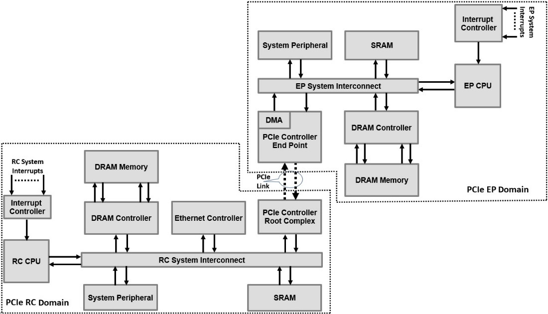
Figure 4.15 – PCIe subsystem sample example
Once the PCIe RC sets up the PCIe subsystem following the topology hierarchy discovery and the EP configuration, the RC CPU can define a data exchange protocol with the EP CPU. The RC CPU defines a memory region in its DRAM memory space and configures the required security access attributes so the EP CPU can access it. The RC CPU may specify, for example, two circular buffers in its DRAM memory space, one for the control data and another for the payload data. It then writes the base address of these circular buffers into a predefined memory address within the PCIe EP domain. These two circular buffers can be used to implement a data transport mechanism between the RC CPU and the EP CPU over the PCIe interface. Assuming that the EP CPU is the data producer, it will then use the PCIe EP DMA engine to write the data from the PCIe EP domain DRAM memory space into the PCIe RC domain DRAM memory space. The DMA descriptors are preset by the RC CPU in its DRAM control data circular buffer, and the pointer to it is already written in a known location by the RC CPU in the EP PCIe domain DRAM memory. The EP CPU sets the PCIe EP controller DMA to read the entries from the remote circular buffer; we assume that the number of entries is preset to N descriptors. Once the PCIe EP controller DMA engine reads the N x DMA descriptors from the control data circular buffer, it notifies the EP CPU via an interrupt. At this moment, the EP CPU has the necessary preset DMA descriptors in its local DRAM memory space; it may need to add the local pointers to the local source of the data. The EP CPU then sets the DMA engine of the PCIe EP controller using the final version of the N x DMA descriptors and arms it when the data itself to transfer is ready. Once the DMA operations are finished, the data is transferred over the PCIe link to the RC PCIe domain DRAM memory space using the destination addresses initially set by the RC CPU. Usually, a notification mechanism via a message-based interrupt is sent from the EP CPU to the RC CPU over PCIe. For more details on message-based interrupts (MSI or MSI-X), please consult the PCIe specification at https://pcisig.com/specifications.
PCIe system performance considerations
Table 4.3 provides the theoretical PCIe link bandwidth; however, these are the line rates that can be achieved at the physical layer. As already introduced, there are overheads that reduce this bandwidth, such as the TLP header and trailer, the data link layer protocol packets used for the link management, and the physical layer symbols. The PCIe generation physical layer encoding scheme, such as 8b/10b in Gen1 and Gen2, as well as 128b/132b in Gen3, Gen4, and Gen5, also introduces a performance degradation in terms of the data throughput. There are also system-level aspects that affect the PCIe system performance such as the maximum payload size (MPS), which defines the maximum payload data size that can be moved at any moment by a single TLP transaction, be it a MRd or a memory write (MWr); it has a maximum of 4,096 bytes and usually, it is set by the PCIe RC to a lower value in SoC applications such as 128 bytes or 256 bytes. There is also the maximum read request size (MRRS), which defines the maximum payload data size that can be requested in a single MRd TLP transaction. Another setting is the read completion (RdC), which specifies the CplD TLP MPS that can be transferred at a time as a response to an MRd TLP request; the RdC is usually set to 64 or 128 bytes in SoC-based applications using PCIe as a system interconnect. When the RC is lower than the MRRS, the PCIe completer uses as many CplD TLPs as needed to fulfill the MRd request.
Information
For further details and how to theoretically estimate the PCIe read and write effective throughput, you can use the following white paper at https://docs.xilinx.com/v/u/en-US/wp350.
Ethernet interconnect
Ethernet-based interconnect is a mature networking protocol, but it keeps evolving in terms of features, physical transport mediums, and connection speeds. It is also one of the simple interfaces that can be used to connect two subsystems together and allow them to share data using a mature connectivity solution. The Ethernet protocol first appeared in 1980, and it was formally standardized under IEEE 802.3 in 1983. We cover Ethernet as an SoC interface because it is included in the Xilinx SoCs covered in this book; it can also allow us to connect two SoCs using the low-level Ethernet protocol as a data transport mechanism, by using a software TCP/IP stack running on an operating system on the Zynq SoC CPUs, or by defining a light data sharing protocol that can use the Ethernet protocol as a transport layer. We will cover communication applications in more detail in the advanced section of this book. In this chapter, we will introduce the Ethernet protocol and the Zynq-7000 SoC Ethernet controller.
Ethernet speeds historical evolution
Since its first appearance in the early 1980s, Ethernet speeds have seen a huge evolution from the initial few MB/s to the currently available hundreds of GB/s speeds. The following table provides a historical overview of the Ethernet theoretical bandwidths:
|
Ethernet version |
Speed |
Introduction year |
|
Ethernet (10Base-X) |
10 Mb/s |
1980 |
|
Fast Ethernet (100Base-X) |
100 Mb/s |
1995 |
|
Gigabit Ethernet (1000Base-X) |
1 Gb/s |
1998 |
|
2.5 Gigabit Ethernet (2.5GBase-T) |
2.5 Gb/s |
2016 |
|
5 Gigabit Ethernet (5GBase-T) |
5 Gb/s |
2016 |
|
10 Gigabit Ethernet (10GBase-X) |
10 Gb/s |
2002 – 2006 |
|
25 Gigabit Ethernet (25GBase-X) |
25 Gb/s |
2016 |
|
40 Gigabit Ethernet (40GBase-X) (1) |
40 Gb/s |
2010 |
|
50 Gigabit Ethernet (50GBase-X) |
50 Gb/s |
2016 |
|
100 Gigabit Ethernet (100GBase-X) (2) |
100 Gb/s |
2010 – 2018 |
|
200 Gigabit Ethernet (100GBase-X) |
200 Gb/s |
2017 |
|
400 Gigabit Ethernet (100GBase-X) |
400 Gb/s |
2017 |
Table 4.7 – Ethernet speeds historical evolution
(1) As 4x 10GBase-X
(2) As 10x 10GBase-X or 4x 25GBase-X
Ethernet protocol overview
Ethernet communication uses Ethernet frames at the data link layer of Open Systems Interconnect (OSI) to exchange data between a source node and a destination node. For more information on the OSI model, please consult https://www.iso.org/obp/ui/#iso:std:iso-iec:7498:-1:ed-1:v2:en.
An Ethernet frame is composed of an Ethernet header, the payload data, and a frame check sequence (FCS) field, which is a CRC used to protect the Ethernet frame from errors while transmitted and received between two Ethernet nodes. At the physical layer, Ethernet adds a preamble field and a start frame delimiter at the start of the Ethernet frame and an interpacket gap field at the end of the Ethernet frame. The following diagram illustrates the Ethernet frame, both at the data link layer and the physical layer levels:
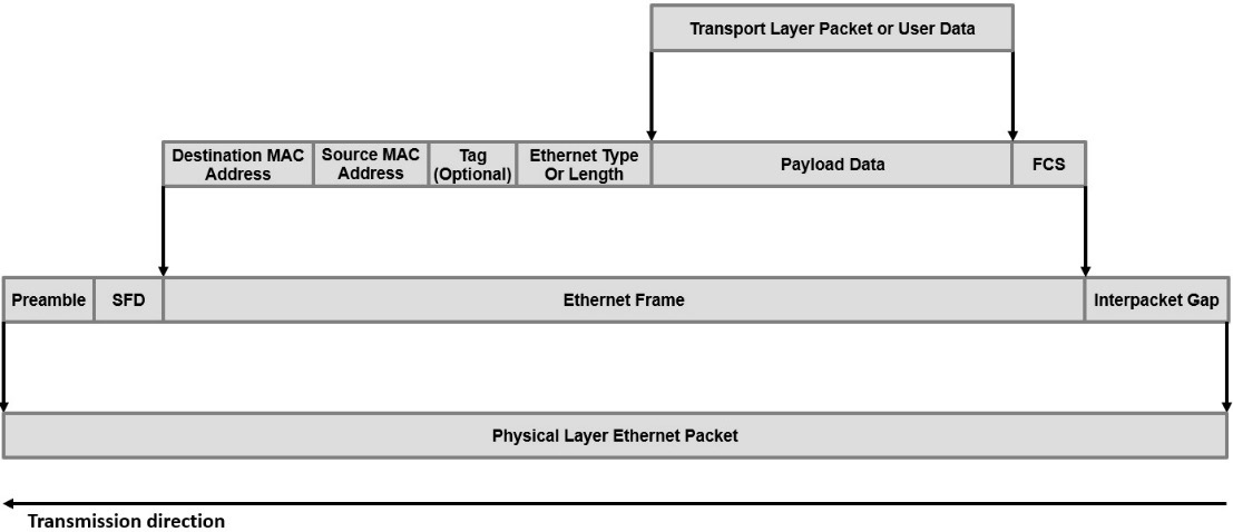
Figure 4.16 – Ethernet frames format
The Ethernet header has many fields, as described in the following table:
|
Field Name |
Size (bytes) |
Description |
|
Preamble |
7 |
A pattern of 0b0 and 0b1 used for the receiver clock synchronization. |
|
Start of Frame Delimiter |
1 |
Byte-level synchronization and a new frame delimiter, which uses the value 0xD5. |
|
Destination MAC Address |
6 |
The destination MAC address, which is used for Ethernet frame delivery purposes. |
|
Source MAC Address |
6 |
The source MAC address, which provides the source of the frame. |
|
Tag |
4 |
This is an optional field and when present, indicates the VLAN. |
|
Ethernet Type or Length |
2 |
When this value is 1,500 or smaller, it indicates the length of the payload in bytes. When it is 1,536 or greater, it is the Ethernet Type (EtherType), indicating which protocol is encapsulated under the payload data. |
|
Payload data |
42 or 46 – 1,500 |
Payload data: a minimum of 42 bytes when the frame is tagged, otherwise, a minimum of 46 bytes. The payload could be user data or a frame from a higher-level protocol. |
|
Frame Check Sequence |
4 |
CRC computed over the entire frame for error protection during transmission. |
|
Interpacket Gap |
12 |
This is the minimum idle time between consecutive packets. |
Table 4.8 – Ethernet packet fields description
For further details on the Ethernet protocol, you are encouraged to study the IEEE 802.3 specification available at https://standards.ieee.org/ieee/8802-3/10556/802.3/7071/.
Ethernet interface of the Zynq-7000 SoC overview
The Zynq-7000 SoC includes an Ethernet interface capable of operating at three speeds: 10 Mb/s, 100 Mb/s, or 1 Gb/s. This Ethernet MAC is capable of operating in full-duplex mode or in half-duplex mode, depending on the link partner to which it is attached. There are two independent Ethernet MAC controllers in the Zynq-7000 SoC. The Ethernet PHY is provided by a separate external chip to the SoC and can be connected to the SoC via a 24-pin interface called the Gigabit Media Independent Interface (GMII). This requires the use of the External Multiplexed Input/Output (EMIO) through the FPGA programmable logic side or via a 12-pin interface called the Reduced Gigabit Media-Independent Interface (RGMII) when using the PS’s Multiplexed Input/Output (MIO). For further details on the Ethernet PHY GMII and RGMII interfaces and their specifications, you can consult the IEEE standard 802.3-2008, Part 3: Carrier Sense Multiple Access with Collision Detection (CSMA/CD) access method and Physical Layer specifications at https://standards.ieee.org/ieee/8802-3/10556/802.3/7071/.
Information
For further details on the EMIO and MIO multiplexed I/O that can be connected to the Zynq-7000 SoC PS, please consult the Zynq-7000 SoC Technical Reference Manual at https://docs.xilinx.com/v/u/en-US/ug585-Zynq-7000-TRM.
The Ethernet controller has an integrated DMA engine that interfaces to the SoC system memory through an AHB master interface. Additionally, it has an APB slave interface through which the PS CPU can configure the Ethernet MAC and check its operating status at runtime.
The following diagram provides a micro-architectural-level view of the Zynq-7000 SoC Ethernet controller:
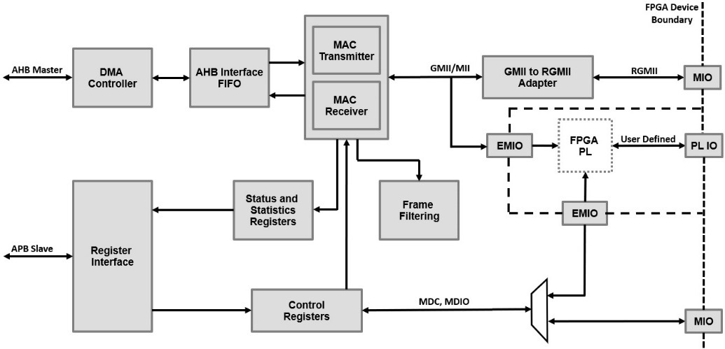
Figure 4.17 – Zynq-7000 SoC Ethernet controller microarchitecture
The DMA engine uses a list of buffer descriptors that software running on the PS CPU prepares for the DMA engine to use when transmit or receive Ethernet operations are started. There are two channels within the DMA engine, one channel for receive and another channel for transmit operations. Each channel has its own list of DMA descriptors. The DMA descriptors are continuous in the PS CPU memory space with the option to wrap when the list reaches its end. Each list is indicated by the PS CPU to the DMA channel engine via a programmable register. Each descriptor has an ownership bit that allows descriptor recycling, meaning that for the receive path, when the software consumes the buffer pointed to by the descriptor, the CPU flips the ownership field, indicating to the DMA engine that it has consumed the buffer pointed to by this descriptor and that now, the DMA engine is allowed to reuse it; if not, then the DMA engine will not. For the transmit direction, software should reuse the DMA descriptor only when it has been transmitted and the ownership bit has been reset accordingly by the DMA transmit engine. For more details on the DMA descriptors and the Ethernet controllers included in the Zynq-7000 SoC, please consult section 16 of the Zynq-7000 SoC Technical Reference Manual at https://docs.xilinx.com/v/u/en-US/ug585-Zynq-7000-TRM.
Introduction to the Gen-Z protocol
This section introduces the Gen-Z standard, an emerging memory-semantic protocol that aims to standardize memory and storage accesses and share them between CPUs, graphic processing units (GPUs), and accelerators in heterogeneous systems. This initiative is led by an industry consortium formed 5 years ago by 12 companies; for more information about the Gen-Z Consortium and its forming member companies, please check https://genzconsortium.org/.
Gen-Z itself is now in the process of being integrated into the Compute Express Link (CXL) standard developed by the CXL Consortium; for more details on the CXL protocol, please check https://www.computeexpresslink.org/about-cxl.
Gen-Z protocol architectural features
The Gen-Z protocol decouples the load-and-store operations from the local controller and interposes the Gen-Z as a fabric in between them. The following diagram illustrates the main architectural concept of the Gen-Z fabric:

Figure 4.18 – Gen-Z fabric’s main architectural concept
With this decoupling, the CPU to memory byte-addressable load-and-store model can be extended to the entire system, where the load-and-store requests are transported first over the fabric, then addressed or translated locally within the media controller. This is possible in modern SoCs where the speed and throughput of the interconnect and the media controllers are high enough to make sharing data using this approach in modern heterogeneous system architectures a potential optimal solution in terms of silicon cost and power consumption. The Gen-Z fabric supports asymmetric data paths, where the read path can be wider than the write path, and vice versa. Access can be local and distributed over memory locally within the system or relatively remotely over a network when access latency makes sense and networked sharing is the optimal option. Gen-Z supports data rates at 16, 25, 32, 56, and 112 GT/s. The Gen-Z protocol abstracts the media type from the fabric as such making access to DRAM, Flash, and storage class memory load-and-store operations uniform providing more flexibility and wider choices for modern SoC designs. The media controllers become abstracted and get located within the local media domain than being interlocked with the CPU or any other compute node. This approach also allows load-and-store operations to be switchable beyond the SoC local interconnect, and the extra added latency will be dependent on the underlying physical layer upon which the Gen-Z will be transported.
The Gen-Z protocol uses memory semantic operations defined using OpCodes and OpClasses that optimize the data transfers and minimize the SoC interconnect utilization as such reducing the overall system power requirements for the same performance in legacy systems. For example, data from the SoC DRAM can be moved to Flash memory in one load and one store operation using the corresponding OpCode/OpClass Gen-Z commands. This also makes the future generation SoCs more scalable and modulable as compute and storage resources can be added without re-architecting the SoC if the need arises in the future, now that compute and storage elements have become plug-and-play to a certain extent and are becoming easily tailored to the specific new system needs.
Gen-Z additionally promotes system low latency by eliminating the need for software stack layers to perform the media-specific translations. This is operationally now offloaded to the media-specific controller sitting behind the Gen-Z fabric that only requires a common load-and-store command regardless of the media-specific access patterns and access latencies.
SoC design and Gen-Z fabric
Building an SoC that can benefit from the Gen-Z features while it is still maturing as a new industry standard requires careful consideration, but it is still a good idea to continue following its evolution. Modern SoC architecture definitions will be faced with challenges that the Gen-Z protocol can help solve; in doing so, there is a need to find suitable Gen-Z controller intellectual property (IP). This will require media controllers, fabric switches, and Gen-Z interfaces; these are most likely already available from a few vendors and can also be considered as a design activity worth engaging in. There is also the Gen-Z PHY mediums to choose from, and the existing first system implementations will make use of mature non-return-to-zero (NRZ) transceivers with their achievable high speeds and very good reliability, such as PCIe PHY at 16 and 32 GT/s, and the Ethernet PHYs at 25 GT/s. There is also the need for verification IPs and FPGA-based prototyping solutions, which are also starting to be announced by members of the Gen-Z Consortium.
CCIX protocol and off-chip data coherency
The CCIX protocol is a chip-to-chip data coherent protocol that enables one or more interconnected nodes to share data in a cache-coherent manner without the need for any software cache maintenance operations. It has been developed by the CCIX Consortium to solve the need for the emerging heterogeneous systems architecture driven by the immense data processing needs of modern SoCs in many emerging applications such as big data, autonomous driving, IoT, machine learning, and artificial intelligence. The CCIX Consortium includes 6 industry promotors, 14 contributing companies, and 16 industry adopters at present. For more information about the CCIX Consortium, please check https://www.ccixconsortium.com/.
CCIX protocol architectural features
The CCIX Consortium has been focusing on building an Instruction Set Architecture (ISA) independent data coherency protocol that can be used to connect accelerators such as GPUs and hardware accelerators (built within FPGAs or in custom-made ASICs) to SoCs using different CPU architectures. CCIX also supports inter-chip virtual addressing modes so data sharing can pass pointers from application-level layers without the need to linearize the data in memory by using in-place DMA operations that add latency and consume more energy. The architectural concept of the CCIX protocol is illustrated in the following diagram:

Figure 4.19 – CCIX protocol architectural concept
The CCIX protocol has a layered architecture that sits on top of the PCIe data link layer. The CCIX protocol doesn’t use the PCIe transaction layer, but rather defines three more stacked components, as illustrated in the following diagram:
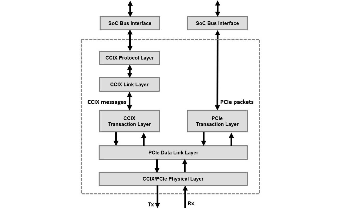
Figure 4.20 – CCIX protocol layers
The CCIX protocol specification is divided into two main sections. The first is the CCIX protocol itself, which defines the inter-chip cache-coherent protocol, the messaging layer, and the flow control mechanisms; the second specifies the CCIX link layers that transport them.
The CCIX link layers or transport specifications are composed of the CCIX and PCIe transaction layers, the PCIe data link layer, and the CCIX physical layer.
CCIX protocol layer
The cache coherency protocol is implemented by the CCIX protocol layer, and it is the top portion of the CCIX standard responsible for MRd and MWr. This layer provides a mapping for the on-chip cache coherency protocol such as the ARM Advanced Microcontroller Bus Architecture (AMBA) Cache-Coherent Hub (CHI). The cache states defined by this layer allow the cache coherency hardware to determine whether a given cache line in a CPU or any accelerator hardware is clean or dirty, and unique or shared. SoC cache coherency has been covered by Chapter 3, Basic and Advanced On-Chip Busses and Interconnects, of this book. For more information on the ARM AMBA CHI protocol, you are encouraged to consult the AMBA specification at https://developer.arm.com/architectures/system-architectures/amba/specifications.
CCIX link layer
This layer is below the CCIX protocol layer, and it formats the CCIX commands for the transport layer in use. In the current revision of the CCIX specification (revision 1.1), the transport layer is based on PCIe.
CCIX and PCIe transaction layer
The CCIX traffic is assigned its own virtual channel (VC) that differentiates it from the PCIe traffic, which is assigned to other VCs. This approach allows the CCIX traffic and PCIe traffic from the upper layers to share the same PCIe controller and the same PCIe link. The CCIX protocol can use the standard PCIe packet formats, but it can also map to its own optimized packet formats, which eliminates many unneeded fields in the PCIe packet header.
PCIe data link layer
The CCIX protocol uses the PCIe data link layer as it is. As already covered in this chapter, the PCIe data link layer performs the PCIe/CCIX link management operations as well as transporting the PCIe/CCIX TLPs by adding an error checking mechanism using the LCRC.
CCIX/PCIe physical layer
The CCIX physical layer supports all the PCIe speeds up to Gen5, that is, 2.5 GT/s, 5 GT/s, 8 GT/s, 16 GT/s, and 32 GT/s. CCIX also adds support for 20 GT/s and 25 GT/s.
Information
For a detailed introduction to the CCIX protocol architecture, you are encouraged to study the white paper at https://www.ccixconsortium.com/wp-content/uploads/2019/11/CCIX-White-Paper-Rev111219.pdf.
Summary
This chapter began by giving an overview of the buses and interconnects used off-chip to connect an FPGA-based SoC to other high-speed devices on the electronics board. It looked at two legacy system buses: the SPI and the I2C. It provided a detailed overview of the PCIe interconnect, its stacked protocol layers, and systems consideration aspects in terms of performance and application-level usage. It then introduced the Ethernet protocol and its suitability to interconnect SoCs on a system or network them using higher software middleware layers such as the TCP/IP protocol. The chapter also looked at the emerging Gen-Z protocol and its concept of using a uniform semantic to access memory over a fabric and remove the CPU to memory and to any storage media interlock. We also covered the emerging CCIX cache-coherent interconnect protocol and the concept of extending data coherency off-chip by adding the necessary protocol layers to manage it in hardware and then transporting it around the system beyond the SoC boundaries over PCIe, for example. The chapter covered the tight link between the PCIe protocol layers and the CCIX protocol layers and how they can be merged and use the same data link and physical layers by exploiting the PCIe protocol QoS and its VCs.
In the next chapter, we will continue introducing the main SoC interfaces required to manage and use internal and external system resources such as internal and external memory and storage. We will also cover most of the communication interfaces available within the Xilinx Zynq-7000 SoC.
Questions
Answer the following questions for rest your knowledge of this chapter:
- Describe the main features of the SPI bus protocol.
- How can the I2C bus protocol interconnect a system with many masters and several slaves?
- What are the layers of the PCIe protocol stack?
- What are the supported speeds and widths of the PCIe link?
- What are the main components in a PCIe RC? How many PCIe RCs can a PCIe system have?
- What are the PCIe maximum payload size, maximum read request size, and read completion? What is the relationship between them?
- How can the read completion affect the read performance over PCIe at a system level?
- Describe how a payload size of 9,000 bytes can be written from DRAM memory in a PCIe end point node, using its DMA engine, into DRAM memory within a PCIe RC node.
- What are the main architectural features of the Ethernet protocol?
- How can Ethernet interconnect two SoCs and move data between them without using any higher-level middleware or TCP/IP stacks?
- What are the main purposes of the Gen-Z protocol? Who owns it?
- How can the Gen-Z protocol improve the system performance of a memory-centric application? Provide an example with a simple quantitative analysis.
- Describe the CCIX protocol and its main architectural features.
- Who owns the CCIX protocol? When can it be used?
- What is the performance improvement that the CCIX protocol can bring to a system with multiple CPUs using different ISAs, and multiple accelerators using internal caches? Provide a quantitative analysis on a simple example you can think of.
- Which PCIe protocol layers are common between the PCIe and CCIX protocols? How can they share the same medium although they are different protocols serving different application layers?