
10
Building a Complex SoC Hardware Targeting an FPGA
In this opening chapter of Part 3, you will be introduced to some of the advanced topics of SoC design that present many challenges to design engineers given their multidimensional nature. It will continue with the same practical approach as Part 2 of this book by adding more complex elements to the hardware design. The hardware will also be built to be able to host an embedded Operating System (OS). You will learn how to use advanced hardware acceleration techniques to help augment the system performance, and you will be equipped with the required fundamental knowledge that makes this design step less challenging. You will examine the different ways these techniques can be applied at the system level, and what aspects need considering at the architectural step in the shared data paradigm.
In this chapter, we’re going to cover the following main topics:
- Building a complex SoC subsystem using the Vivado IDE
- System performance analysis and the system quantitative studies
- Addressing the system coherency and using the Cortex-A9 ACP
Technical requirements
The GitHub repo for this title can be found here: https://github.com/PacktPublishing/Architecting-and-Building-High-Speed-SoCs.
Code in Action videos for this chapter: http://bit.ly/3TlFU1I.
Building a complex SoC subsystem using Vivado IDE
We will start from the Electronic Trading System (ETS) SoC hardware design and add more features to it, such as connecting a master interface from within the Programmable Logic (PL) side of the FPGA SoC to the Accelerator Coherency Port (ACP) of the Processing Subsystem (PS) side. We will also make sure that the PS design includes all the hardware features necessary to run an embedded OS such as the timers, the storage devices, the Input/Output (IO) peripherals, and the communication interfaces. Let’s get started:
- Launch the Vivado IDE and open the ETS SoC hardware design we built in Chapter 7, FPGA SoC Hardware Design and Verification Flow.
- Go to IP Integrator and click Open Block Design, causing the block design to open in the Vivado IP Integrator window.
- Double-click on ZYNQ7 Processing System to open it for customization. The following window shall open:

Figure 10.1 – ETS SoC PS block diagram
- Double-click on 64b AXI ACP Slave Ports in the ETS SoC PS block to access the ACP port configuration interface. This will open the PS-PL Configuration window shown in the following screenshot. In the ACP Slave AXI Interface row, check both rows associated with the ACP port configuration. We will cover the ACP details later in this chapter.
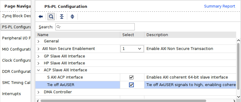
Figure 10.2 – Configuring the ACP slave AXI interface in the Vivado IDE
- Expand the General row and check the Include ACP transaction checker option, as shown in the following figure:
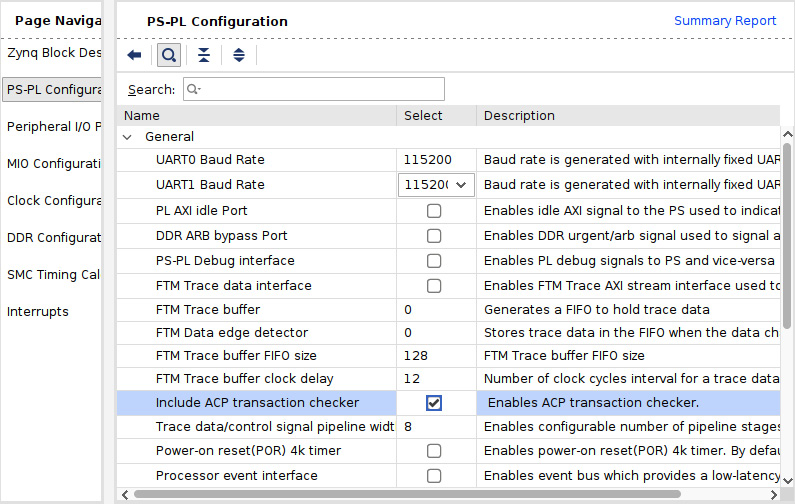
Figure 10.3 – Enabling the ACP transaction checker for the ACP port
- We need to connect the ACP slave AXI port to the MicroBlaze subsystem interconnect. This step is performed semi-automatically by clicking on the IP Integrator Run Connection Automation hyperlink:

Figure 10.4 – Using Run Connection Automation to connect the ACP port

Figure 10.5 – ACP slave port connection wizard
- We need to add the SD IO peripheral to the PS subsystem. Double-click on Zynq Block Design in the IP Navigator pane to open the ZYNQ7 Processing System diagram, as shown in Figure 10.6.
- Double-click in the SD 0 row in the IO Peripherals column to add the SD card to the PS system. This may be used to host the filesystem of the OS if needed later by the advanced software development flow.
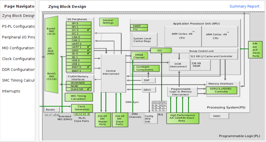
Figure 10.6 – Adding the SD IO to the PS subsystem in the Vivado IDE
- We have included everything we need in the ETS SoC hardware to study some advanced features of the SoC hardware design flow, as well as preparing the ETS SoC hardware to host an embedded OS. We need to make sure that the ACP port is mapped and visible within the MicroBlaze address map so the MicroBlaze CPU can initiate transactions through the PS ACP port.
- Open the address map by clicking the Address Map tab in the IP Integrator window. The system address map should open. Expand all the entries in it and make sure that you include and assign the ACP region, as shown:
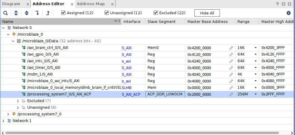
Figure 10.7 – Adding the ACP slave port to the MicroBlaze subsystem address map
- Click on Validate Design using the Vivado IDE main menu, as shown. This should not raise any errors:
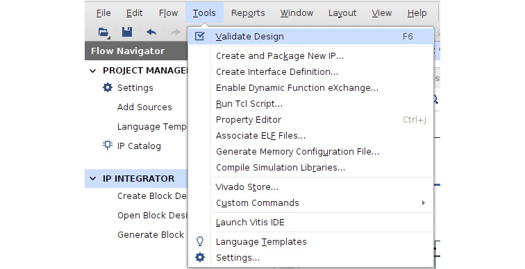
Figure 10.8 – Validating the ETS SoC design in Vivado IDE
System performance analysis and the system quantitative studies
To perform the SoC system performance analysis and quantitively study it, we need to refer to Chapter 8, FPGA SoC Software Design Flow, specifically, all the details from the section titled Defining the distributed software microarchitecture for the ETS SoC processors. We have provided a full ETS SoC microarchitecture, as shown in the following diagram:

Figure 10.9 – ETS SoC microarchitecture simplified diagram
In this analysis, we aim to understand whether the proposed IPC between the Cortex-A9 CPU and the MicroBlaze PP processor mechanism is optimal and using all the possible hardware capabilities of the SoC FPGAs. We would like to figure out whether using the ACP would be a better alternative to using the microarchitecture proposal implementation via the PS AXI GP interface. The current IPC mechanism from the Cortex-A9 toward the MicroBlaze PP uses the circular buffer queue hosted in the AXI BRAM, where the Acceleration Requests (AREs) are built by the Cortex-A9 first and then written as entries into the ARE circular buffer. This is followed by a notification from the Cortex-A9 to the MicroBlaze PP as an interrupt by writing to the AXI INTC0. Once the MicroBlaze PP reaches the ARE entry, it uses the pointers in it to retrieve the Ethernet frame to filter from where the Ethernet DMA engine has written it, and these are in the OCM memory. The following figure summarizes this interaction with the sequencing of events details:

Figure 10.10 – ETS SoC Cortex-A9 and MicroBlaze PP IPC data flow and notification sequencing
The ETS SoC Cortex-A9 and MicroBlaze PP IPC data flow and the notification sequencing include the following steps:
- When the Ethernet DMA engine receives an Ethernet frame, it uses the details provided by the Cortex-A9 CPU to copy the payload data of the Ethernet frame from the Ethernet controller buffer into the OCM memory. This operation to read the descriptor entry from the AXI BRAM by the DMA engine takes 6 Clock Cycles (CCs) of the PS interconnect clock (ps_clk), which is [6 x CC (ps_clk)].
- The Cortex-A9 receives a notification from the Ethernet controller DMA engine for the received Ethernet frame. It reads the Ethernet DMA descriptor entry and uses the OCM memory pointer of the Ethernet frame to inspect its type. The preceding flow ignores the Cortex-A9 partial access to the Ethernet frame in the OCM memory as it is considered negligible and not affecting this specific analysis’ outcome. This may take 8 CCs of the MicroBlaze PP system clock (pl_clk), which is [8 x CC (pl_clk)].
- When the Cortex-A9 finds that the Ethernet frame is for a UDP packet, it constructs an ARE[i] for it in the AXI BRAM. This processing is internal within the Cortex-A9 core and may take n CCs of the Cortex-A9 clock, which is [n x CC (ca9_clk)].
- The Cortex-A9 notifies the MicroBlaze by writing to the AXI INTC0 (AXI INTC is the Xilinx AXI interrupt controller, which combines several interrupts into a single interrupt to notify the MicroBlaze processor), which generates an interrupt for the MicroBlaze PP. This is an access to a register within the AXI INTC0 running at the MicroBlaze system clock and may take in the region of 6 CCs MicroBlaze system clock, which is [6 x CC (pl_clk)].
- Once the MicroBlaze PP reaches the ARE[i], it reads from the AXI BRAM to retrieve the pointer to use to read the important fields of the Ethernet frame from the OCM memory. It may take in the region of 4 CCs MicroBlaze system clock, which is [4 x CC (pl_clk)].
- The MicroBlaze PP now reads the fields of interest using the information in the ARE[i]. This will be performed a field at a time followed by the necessary computation to perform the requested filtering. If we only consider the access time of the data, the cumulative time to access it would be approximately 6 CCs per word of 32 bits each; in total, we have 12 words, which results in [72 x CC (pl_clk)].
- Once the results are ready, the MicroBlaze PP will create an entry in the appropriate queue in the OCM and/or the AXI BRAM, and this will take approximately 6 CCs per word of 32 bits each, which is [6 x CC (pl_clk)].
In the preceding approximation, we observe that the time it takes for the IPC communication associated with a single Ethernet frame from its reception by the Ethernet DMA to providing the filtering results is the sum of all the estimated segment’s times:

Obviously, this only includes the IPC times, which is interleaved by the packet inspection time by the MicroBlaze; however, the filtering time is another performance metric we can estimate, but it won’t affect the decision to move into using the ACP in our case.
In the ETS SoC design, we have the following:
- pl_clk = 100 MHz
- ps_clk = 222 MHz
- ca9_clk = 666 MHz
The estimated IPC required time is therefore as follows:


Since [n x CC (ca9_clk)] is roughly the same even if we modify the IPC mechanism used, we can then use the preceding result as a base figure to compare against.
Another point worth highlighting here is that the IPC mechanism dictates the use of non-cacheable memory since the system interconnect isn’t coherent within the PS nor between the PS and the PL. If cacheable memory regions are used for any of the previously involved data in the IPC mechanism, cache management operations should be carefully used to flash the Cortex-A9 data cache whenever a descriptor-related field is updated or an ARE is constructed. The use of cache management is fine but will have a hit on the Cortex-A9 CPU performance. We can study this case as an exercise, but we will need to look at the resulting assembly language instructions to be able to estimate the amount of time needed by using the cache management instructions. This is easily done using the emulation platform and running code on it that allows us to view its disassembly associated instructions.
Addressing the system coherency and using the Cortex-A9 ACP port
In this chapter, the focus for the hardware acceleration is to find ways to closely integrate the PL logic hardware accelerator with the Cortex-A9 cluster and build a more direct path between software and the acceleration hardware. This direct path should be without paying the penalty of using non-cacheable memory for data shared between the Cortex-A9 and its hardware accelerators. Using cacheable memory without any cache coherency support from the hardware imposes some performance penalties. Such sharing requires some form of synchronization between the Cortex-A9 and the PL Accelerators; for example, by using cache maintenance operation in the Cortex-A9 software. This is required following every update to the common data variables between the Cortex-A9 software and the PL hardware accelerator. The way this close integration can be achieved in the Zynq-7000 SoC is through the ACP, which provides a direct coherent path from the PL logic accelerator to the Cortex-A9 caches and doesn’t require the Cortex-A9 to use any cache maintenance operations following access to a shared data variable with the PL hardware accelerator. The following diagram provides an overview of the envisaged topology to connect the MicroBlaze PP-based PL hardware accelerator to the PS:

Figure 10.11 – ETS SoC Cortex-A9 and MicroBlaze PP IPC via the ACP
Overview of the Cortex-A9 CPU ACP in the Zynq-7000 SoC FPGA
The ACP is an AXI 64-bit slave port on the PS that allows the PL implemented and mapped masters to access the Cortex-A9 CPU cluster L2 and the OCM memory via transactions that are coherent with the L1 data caches of the Cortex-A9 cores and the L2 common cache. This is possible as the ACP is connected to the Cortex-A9 CPU cluster Snoop Control Unit (SCU). Within the SCU, address filtering is implemented by default that will route transactions targeting the upper 1 MB or the lower 1 MB of the 4 GB system address space to the OCM memory, whereas the remaining addresses are routed to the L2 cache controller.
Information
For more information on the SCU address filtering, please consult Chapter 29 of the Zynq-7000 SoC Technical Reference Manual: https://docs.xilinx.com/v/u/en-US/ug585-Zynq-7000-TRM.
The ACP write Issuing Capability (IC) is three transactions, and its read IC is seven transactions.
The ACP read or write requests can be coherent or non-coherent depending on the setting of the AXI AxUSER[0] and AxCACHE[1] signals, where x can be either R for read or W for write transactions. We distinguish the following request types:
- ACP coherent read requests: When ARUSER[0]=1 and ARCACHE[1]=1, and ARVALID is HIGH. This qualifies the read operation as coherent, and the data is provided directly from the processor cache holding it and returned to the ACP port. When there is no data in any of the cluster caches, the read request is forwarded further to one of the SCU AXI master ports.
- ACP non-coherent read requests: When ARUSER[0]=0 or ARCACHE[1]=0, and ARVALID is HIGH. This doesn’t qualify the request as coherent, and the read request is forwarded to one of the available SCU AXI master ports without looking up the CPU cluster caches.
- ACP coherent write requests: When AWUSER[0]=1 and AWCACHE[1]=1, and AWVALID is HIGH. This qualifies the write operation as coherent. The data, when present in one of the Cortex-A9 caches, is first cleaned and invalidated from the caches. However, if the data is not cached in any of the Cortex-A9 processors, or the cache line holding it has been cleaned and invalidated, the write request is forwarded to one of the SCU AXI master ports. The transaction can be a “write allocate” into the L2 cache if specified by the qualifying signals on the AXI interface.
- ACP non-coherent write requests: When AWUSER[0]=0 or AWCACHE[1]=0, and AWVALID is HIGH. The transaction is not coherent, and the write request is forwarded directly to the SCU AXI master ports.
Implications of using the ACP interface in the ETS SoC design
As already introduced, the ACP interface will allow the use of a cacheable memory to store the data variables shared between the Cortex-A9 and the MicroBlaze PP to implement the IPC data flow and its associated notifications. It is worth noting that the coherency is only in one direction; that is, if the PL master were caching any data, the Cortex-A9 would have no way of knowing whether it has changed without the PL master explicitly notifying it. This is because the AXI bus is not a coherent interconnect. It is only because we are routing transactions first through the Cortex-A9 SCU that we have a way of fulfilling coherent transactions by the Cortex-A9 caches. We can now move all the content of the AXI BRAM to the OCM or DRAM memory and access them coherently through the ACP port of the Cortex-A9. The sequencing diagram showing the different data mappings becomes like the following:

Figure 10.12 – ETS SoC Cortex-A9 and MicroBlaze PP IPC sequencing when using the ACP
Let’s now quantify the ETS SoC Cortex-A9 and MicroBlaze PP IPC data flow and the notification sequencing when using the ACP. We will follow the same method we already established earlier. The sequence includes the following steps:
- When the Ethernet DMA engine receives an Ethernet frame, it uses the details provided by the Cortex-A9 CPU to copy the payload data of the Ethernet frame from the Ethernet controller buffer into the DRAM memory. This operation to read the descriptor entry from the DRAM by the DMA engine takes 4 CCs of the PS interconnect clock (ps_clk), which is [4 x CC (ps_clk)].
- The Cortex-A9 receives a notification from the Ethernet controller DMA engine for the received Ethernet frame. It reads the Ethernet DMA descriptor entry and uses the DRAM memory pointer of the Ethernet frame to inspect its type. The preceding flow ignores the Cortex-A9 partial access to the Ethernet frame in the DRAM memory as it is considered negligible and not affecting this specific analysis outcome. This may take 4 CCs of the PS interconnect clock (ps_clk), which is [4 x CC (ps_clk)].
- When the Cortex-A9 finds that the Ethernet frame is for a UDP packet, it constructs an ARE[i] for it in the DRAM. This processing is internal within the Cortex-A9 core and may take n CCs of the Cortex-A9 clock, which is [n x CC (ca9_clk)].
- The Cortex-A9 notifies the MicroBlaze by writing to the AXI INTC0, which generates an interrupt for the MicroBlaze PP. This is an access to a register within the AXI INTC0 running at the MicroBlaze system clock. It may take in the region of 6 CCs MicroBlaze system clock, which is [6 x CC (pl_clk)].
- Once the MicroBlaze PP reaches the ARE[i], it reads from the DRAM through the Cortex-A9 ACP to retrieve the pointer to use to read the important fields of the Ethernet frame from the DRAM memory. It may take in the region of 4 CCs MicroBlaze system clock, which is [4 x CC (pl_clk)].
- The MicroBlaze PP now reads the fields of interest using the information in the ARE[i]. This will be performed a field at a time followed by the necessary computation to perform the requested filtering. If we only consider the access time of the data from the DRAM via the Cortex-A9 ACP, the cumulative time to access it would be approximately 4 CCs per word of 32 bits each, but the MicroBlaze can issue up to seven consecutive reads before the first read completion is received. However, this is only possible if we are using a data cache on the MicroBlaze PP and therefore, we can issue up to a cache line read at a time (32 bytes). Since we haven’t configured the MicroBlaze PP with a data cache, we will assume a read capability of two words at a time, and therefore, the latency is halved. In total, we have 12 words, which results in [(12 x 4/2) x CC (pl_clk)], which is [24 x CC (pl_clk)].
- Once the results are ready, the MicroBlaze PP will create an entry in the appropriate queue in the DRAM through the Cortex-A9 ACP, and this will take approximately 4 CCs per word of 32 bits each, which is [4 x CC (pl_clk)].
In the preceding approximation, when using the ACP, we observe that the time it takes for the IPC communication associated with a single Ethernet frame from its reception by the Ethernet DMA to providing the filtering results is the sum of all the estimated segment’s times:

Obviously, this only includes the IPC times, which are interleaved by the packet inspection time by the MicroBlaze.
In the ETS SoC design, we have the following:
- pl_clk = 100 MHz
- ps_clk = 222 MHz
- ca9_clk = 666 MHz
The estimated IPC required time is therefore as follows:


Since [n x CC (ca9_clk)] is roughly the same even if we have modified the IPC mechanism used, we can then use the preceding result as a base figure to compare against the previously computed one.
We observe that we have improved the IPC time by 571 nanoseconds. We are also able to use shared SoC memories cacheable by the Cortex-A9 and without the need for cache management operations to maintain the data coherency with the MicroBlaze PP.
In general, using the ACP is beneficial in system designs such as for packet processing, where the IPC latency and caching improve the application performance greatly.
Summary
In this chapter, we added a few hardware elements to the ETS SoC design to prepare it for hosting an embedded OS and improved the IPC communication between the Cortex-A9 CPU and the MicroBlaze PP. We also delved into the system performance analysis by first providing a detailed sequencing diagram of the IPC mechanism and then using it as a base to perform a quantitative study. We have used time estimates to measure how long the IPC communication associated with a received Ethernet frame to filter by the PL logic would cost. We found that a significant amount of time is needed to provide the information for moving the data and its associated descriptors from the PS domain to the PL domain. We studied the case of the IPC mechanism when using the PS AXI GP port and then studied the alternative solution of using the ACP port of the Cortex-A9. We have also exposed the issues of using cacheable memory in these scenarios and how this will require cache management operations when not using the ACP to keep the PS and PL looking and using the same copy of the shared data all the time. We computed that the use of the ACP with its coherency capability greatly reduces the time consumed by the IPC mechanism. We have also looked at most of the technical details of ACP to provide a good overview of its features and supported transactions.
In the next chapter, we will explore more advanced topics of the FPGA-based SoCs, with a focus on security.
Questions
Answer the following questions to test your knowledge of this chapter:
- What are the main features we have added to the ETS SoC design in this chapter and why did we add them?
- Describe the main steps needed to connect the MicroBlaze subsystem to the PS block in Vivado.
- What modifications are needed to the address map and why?
- Which type of transactions are supported by the ACP port?
- List the different steps involved in the Cortex-A9 to the MicroBlaze PP IPC when using the PS AXI GP.
- List the different steps involved in the Cortex-A9 to the MicroBlaze PP IPC when using the PS ACP.
- How does the ACP improve the Cortex-A9 to the MicroBlaze PP IPC performance?
- Describe a scenario (not using the ACP) when cache management operations are needed to keep the data shared between the Cortex-A9 and the MicroBlaze PP coherent.
- List some of the disadvantages of using the ACP in general as a gateway between the PL accelerators and the Cortex-A9 memory space.
- Why is using the ACP the best method for sharing data between the Cortex-A9 and the PL accelerators in packet processing applications such as the ETS SoC?