
3
Basic and Advanced On-Chip Busses and Interconnects
This chapter will begin by providing an overview of the buses and interconnects that are used within an SoC. We will introduce the concepts of data sharing and coherency and how to solve their associated challenges. This will give you a good introduction to the Advance Microcontroller Bus Architecture (AMBA) and the Open Core Protocol (OCP) protocols. Finally, we will cover the data movement within an SoC and how to use DMA engines.
In this chapter, we’re going to cover the following main topics:
- On-chip buses and interconnects overview
- ARM AMBA interconnect protocols suite
- OCP interconnect protocol
- DMA engines and data movements
- Data sharing and coherency challenges
On-chip buses and interconnects overview
FPGA and ASIC-based SoCs are built using multiple components, which are a combination of modules provided as macros by the FPGA vendor, designed in-house usually in RTL, and third-party modules that require a form of licensing to use. These modules are commonly referred to as intellectual properties (IPs). These IPs are connected in a topology specified by the SoC hardware architecture using buses and interconnects. They collaborate, which means they need to interact at runtime to implement a specific set of tasks as part of the system’s overall functionality. There are many levels of functional complexity and features that a given interconnect supports. These are based on a bus protocol specification such as ARM AMBA, OCP, or IBM CoreConnect, to mention a few. In this chapter, we will focus on ARM AMBA, which is a collection of bus protocols grouped under a specific AMBA standard revision. However, we will also cover the OCP bus protocol as it is also common in the ASIC SoC designs and you may need to design OCP to AMBA bridges to integrate third-party IPs that use interfaces based on the OCP protocol specification. You may also be porting an ASIC-based SoC to an FPGA-based SoC for prototyping and/or production. This will also help us compare it to ARM AMBA in terms of functional features and complexity.
On-chip bus overview
The communication bus is the medium over which two interfaces from different IPs communicate. A bus can be as simple as a point-to-point single transaction or a single-threaded connection lane or implemented using a complex many-to-many, multi-threaded, and multi-layer transactions protocol. At one end of the bus, there is a transaction initiator or a master interface while at the other end, there is a target or a slave interface. The initiator puts a data access request on the bus that the target responds to by consuming the write data provided by the initiator or by providing the read data requested by the initiator. A simple bus is usually composed of the following lanes:
- A data lane (or lanes for cases where the read path is different than the write path).
- An address lane to specify the exact storage location of the data in the completer or target’s address space.
- A control lane to qualify the transaction as a read or write and provide synchronization information as to when a given control signal is valid, ready, and so on.
The following diagram illustrates the concept of a simple bus:

Figure 3.1 – Simple point-to-point bus
On-chip interconnects
Interconnects add many functional features to the point-to-point bus, which make them able to connect many buses in a single shared system address space. This usually requires a central switching capability, bus protocol conversion, buffering, and arbitration agent that can dynamically allow a requesting initiator and a target to establish a connection and exchange data, even when they don’t belong to the same bus protocol standard. Interconnect switches differ in complexity from a simple crossbar switch to a Network-on-Chip (NoC) with protocol layers conversion, data coherency, advanced routing capabilities, multi-transactions, and multi-threaded capabilities. The following diagram illustrates the concept of a crossbar switch being used to interconnect multiple IPs using simple buses. The simple features are just like those in a point-to-point simple bus case:

Figure 3.2 – Simple switching matrix-based interconnect
In an NoC, the initiator can be multi-threaded, meaning that multiple hardware threads can share the same bus interface in the NoC. Here, the interconnect can use techniques to track many parallel transactions originating from the same hardware bus interface toward targets, even though they originate from different hardware threads. Every bus protocol that supports this feature has mechanics that allow the NoC, the initiators, and the targets to share the bus medium and fulfill these types of transactions. There is also support for concurrent transactions for both read and write since the bus uses multiple paths for the request phase, the command response phase, and the data phases. In some bus protocols, such as AMBA AXI, there are multiple data paths – one for the read and one for the write, allowing concurrent read and write transactions. It can also issue many of these transactions before waiting for the ongoing ones to complete first, though this is quantitatively limited by the transaction type issuing capability of the initiator, the NoC, and the target. The read and write transactions are also varied and aligned with many kinds of masters, such as DMA engines, processors, and processor caches. The following diagram illustrates the concept of NoC:

Figure 3.3 – Network-on-chip-based interconnect
ARM AMBA interconnect protocols suite
AMBA is a collection of bus and interconnect specifications provided by ARM for use in SoCs to attach initiators to targets with different levels of features and protocol complexity. It is an open standard and free to use in SoCs. The specification can be accessed from the ARM website at https://developer.arm.com/architectures/system-architectures/amba/specifications.
The current revision is revision 5. Historically, each newer revision kept backward compatibility with the previous ones but also added new bus protocols with newer features that were developed to keep pace with the modern SoC complexities and higher performance demands. AMBA had to evolve to support multi-core and multi-cluster CPU topologies, which also use some sort of accelerator with all the challenges they present while maintaining the support for lower performance and simpler SoC topologies. The more complex a hardware system becomes. the more power-hungry it will become. ARM has been providing features that balance all the system Key Performance Indicators (KPIs) to still meet the needs of building complex SoCs.
ARM AMBA standard historical overview
The first AMBA standard or AMBA specification revision 1.0 (AMBA1) was available from ARM in 1996. It included two bus protocols: the Advanced System Bus (ASB) and the Advanced Peripheral Bus (APB). Only the APB bus protocol is still in use in today’s SoCs and mostly for registers access and as a configuration interface for IPs. The second revision of the AMBA specification (AMBA2) was released in 1999 and added the Advance High-performance Bus (AHB) to the existing ASB and APB bus protocols from revision 1.0. Revision 3.0 (AMBA3) was released in 2003 and added the ARM eXtensible Interface (AXI-3) for high-performance data exchanges and ARM Trace Bus (ATB) for trace data encoding and transfer capabilities between elements of ARM CoreSight (ARM’s SoC debug and tracing technology). AMBA revision 4.0 (AMBA4) was first released in 2010 by launching the AXI-4 bus protocol as an upgrade to AXI-3. In 2011, ARM added coherency support, which resulted in the introduction of the AMBA AXI-4 Coherency Extension (ACE) bus protocol. AMBA4 also defines the AXI Streaming protocol, which is used in point-to-point connectivity between IPs for high data transfers. It also added the low power interface specification for clock management and power control. These were known as the Q-Channel and P-Channel interfaces, respectively. The latest AMBA revision is 5.0 (AMBA5), which was released in 2013. It defines the Coherent Hub Interface (CHI) protocol as an interface with the capability to sustain high-performance data exchanges while also interconnecting processors in a cache-coherent way. AMBA5 also upgraded the AXI bus to AXI-5 and, over time, added support for many newer bus protocols, such as the Credited eXtensible Stream (CXS) protocol for point-to-point data exchanges between IPs. AMBA5 introduced the AMBA Adaptive Traffic Profile (ATP) specification, which isn’t a bus interface by itself but rather a qualitative specification associated mainly with the AXI master interfaces in real-time transactions and their timing. AMBA5 includes the AMBA Generic Flash Bus (GFB) specification, which is specifically designed to support non-volatile memories such as flash device transaction types. AMBA5 also includes the AMBA Distributed Translation Interface (DTI), which defines the protocol that’s used by elements of the system memory management units for system-level address translation services within the SoC. The following diagram visualizes the historical evolution of the AMBA standard and summarizes the specific bus and interconnect protocol within each revision of the standard:

Figure 3.4 – AMBA interconnect standards and bus protocol evolution
APB bus protocol overview
This section will explore the APB bus protocol, its evolution throughout the different AMBA standard revisions, and its added features and mechanisms. We will gain an understanding of this bus’s supported transactions, signaling, and application use cases. We will provide an example system implementation using the APB bus.
APB bus protocol evolution
The APB bus is the simplest interface protocol included in the ARM AMBA standard. It has evolved since its first inception in 1996. Every revision added new features and improvements to the protocol while keeping backward compatibility with the previous revisions. APB revision 1.0 is now obsolete and only APB2, APB3, APB4, and APB5 are still active protocols in the industry.
APB2 is considered the base APB protocol for defining the signal interfaces, the read and write supported transactions, and the two APB available components, namely the APB bridge and the APB slave.
The APB3 protocol added support for wait states and transaction error reporting to the base APB2 protocol. The PREADY and PSLVERR signals were added to allow this protocol to expand.
In the APB4 protocol, transaction protection and sparse data transfer features were added. The PPROT signal implements the secure transaction access, so it is used to distinguish between secure and non-secure transactions over the APB bus, while the PSTRB signal implements the write strobe to enable the sparse data write transaction between an AMBA master and an OPB slave.
The APB5 revision extends the APB4 protocol with support for wakeup signaling, user signaling, parity protection, and check signals. These features can enhance the SoC’s power consumption, extend the APB protocol by using custom sideband signaling, and improve reliability in the system.
APB bus characteristics
The APB protocol is a simple interface that requires minimal silicon resources for its implementation in an SoC compared to other AMBA bus protocols, thus making it a low-power bus. Data transfers on the APB bus require a minimum of two clock cycles. The APB bus is designed to be a side or secondary bus through which the CPU can implement a control path, thus avoiding any interference from the main data bus, which is implemented using one of the high performances AMBA buses such as AXI or AHB. At runtime, the CPU can use the APB bus to set up an IP registers file, read the status of IP transactions that have been completed, or any other control path-related tasks that software can easily split from the data path to free it for high throughput access, such as I/O packet data or memory data structures through the CPU caches. The IP APB ports are usually grouped as a tree of up to 16 ports that hang off an APB bridge from the main SoC interconnect. The APB bridge performs the transactions protocol conversion and mapping. The APB bridge acts as the transaction’s initiator in this topology, while the APB slave behaves as the target that responds to these transactions. The APB specification also refers to the APB bridge as the Requester and the APB slave or target as the Completer.
APB bus interface signals
The following diagram illustrates the connectivity between an APB Requester and an APB Completer, where all the signals defined by APB5 are present:

Figure 3.5 – APB bus interface signals
As shown in the preceding diagram, the APB bus signals are split into three categories: the Requester-driven data lane and signals, the Completer-driven data lane and signals, and the SoC bus clock and reset signals. The following table provides a short description of the Requester signals:
|
Signal |
Width |
Description |
|
PADDR |
32 |
Address Lane, driven by the Requester. |
|
PPROT |
3 |
Protection type control signal. It indicates if this is a normal, privileged, or secure operation. It is also used to indicate if this is data or instruction access. |
|
PSELx |
1 |
Select signal. Indicates to the Completer that it has been selected by the Requester to respond to an incoming transaction. |
|
PENABLE |
1 |
Enable signal. It is set to indicate the start of the second cycle in an APB transaction. |
|
PWRITE |
1 |
Transaction direction. When HIGH, it is a Write; when LOW, it is a Read. |
|
PWDATA |
DW |
Write the data lane of DW width. The Requester uses this lane to place the write data that targets the Completer. DW is usually 8, 16, or 32 bits. |
|
PSTRB |
DW/8 |
Write strobe signals. Each signal indicates that the corresponding data byte is valid. |
|
PWAKEUP |
1 |
Wake-up signal. This signal is used by the Requester to indicate activities associated with this APB interface. |
|
PAUSER |
URW |
User-defined request attribute lane. This lane can be used to extend the APB protocol and customize it to support other features and attributes not defined by the APB5 protocol. This lane represents the request phase of a custom-defined transaction. |
|
PWUSER |
UDW |
User-defined write attribute lane. This lane can be used to extend the APB protocol and customize it to support other features and attributes not defined by the APB5 protocol. This lane can carry the write data from the Requester to the Completer of an APB custom-defined write transaction. |
Table 3.1 – APB bus interface signals description
The following table provides a short description of the Completer signals:
|
Signal |
Width |
Description |
|
PREADY |
1 |
Ready signal. This signal is used by the Completer to qualify or extend the APB transaction on the bus. |
|
PRDATA |
DW |
Read data lane. Used by the addressed Completer to provide the requested read data. It is usually 8, 16, or 32 bits wide. |
|
PSLVERR |
1 |
Transfer error signal. Used by the slave to indicate the transaction completion status to the Requester. |
|
PRUSER |
UDW |
User-defined read attribute lane. This lane can be used to extend the APB protocol and customize it to support other features and attributes not defined by the APB5 protocol. This lane can carry the read data returned by the Completer to the Requester of an APB custom-defined read transaction. |
|
PBUSER |
URW |
User-defined response attribute lane. This lane can be used to extend the APB protocol and customize it to support other features and attributes not defined by the APB5 protocol. This lane represents the response phase of a custom-defined transaction. |
Table 3.2 – APB bus interface Completer signals description
The following table lists the SoC signals:
|
Signal |
Width |
Description |
|
PCLK |
1 |
Clock signal. This is a common signal provided by the SoC to both the Requester and Completers. |
|
PRESETn |
1 |
Reset signal. This is a common active LOW signal provided by the SoC to both the Requester and Completers. |
Table 3.3 – APB bus interface SoC signals description
APB bus-supported transactions
The APB bus’s latest protocol – that is, APB5 – defines the following transaction types:
- Write transactions without the Wait state
- Write transactions with Wait state insertion
- Read transactions without the Wait state
- Read transactions with Wait state insertion
- Write transactions with Write strobes
- Error response
- Secure and non-secure transactions
- Wake-up transaction signaling
- User signaling
This section only attempts to provide a functional overview of the preceding supported transactions in APB5. You are encouraged to study the AMBA5 standard that defines the APB5 bus protocol for further implementation details. The APB5 bus protocol can be found at https://developer.arm.com/documentation/ihi0024/latest/.
Write and read transactions are simple back-to-back transactions that are set by the Requester in a predefined manner so that the Completer can sense them and decode the transaction accordingly. Data is then accepted from the write lane or provided on the read lane to the Requester. As mentioned previously, the APB bus is a simple transaction bus with no pipelining or burst support. The protection support is worth highlighting as it adds an orthogonal qualification to the transaction using the PPROT bits, as follows:
- PPROT[0]: This indicates if this is a Normal or Privileged transaction and usually reflects the status of the running state of the Requester. It can easily be mapped by the CPU to its execution state (kernel mode or user mode, for example).
- PPROT[1]: Secure or non-secure. This signal can be used to implement hardware security by allowing access to certain registers when the transaction is classified as secure – that is, PPROT[1] is LOW. When PPROT[1] is set to HIGH by the Requester, access to secure registers, for example, is prohibited by the Completer.
- PPROT[2]: Data or instruction. This signal provides a hint regarding the type of data exchanged by the transaction.
APB bus example system implementation
As mentioned previously in this section, the APB Requester is an APB bridge that translates an upstream protocol, such as AHB or AXI, into an APB bus protocol to provide a control path to a CPU through which it can set up IP peripheral registers and check the runtime status following an interrupt event, for example. The following diagram provides an overview of such an implementation, where the APB bus is connected to the SoC interconnect through an AXI to APB bridge:

Figure 3.6 – APB bus example system implementation
AXI bus protocol overview
This section will explore the AXI bus protocol, its evolution throughout the different AMBA standard revisions, and its added features and mechanisms. We will gain an understanding of this bus’s supported transactions, signaling, and application use cases. We will provide an example system implementation using the AXI bus. This section tries to provide a detailed enough overview of the AXI-3 and AXI-4 bus protocols as these are used in the Zynq-7000 SoC and Zynq UltraScale+ SoC FPGAs. AXI-5 is mentioned for completeness only, but you are still encouraged to study it using the previously mentioned AMBA5 standard specification from ARM.
AXI bus protocol evolution
As illustrated in Figure 3.4, the AXI bus protocol first appeared in the AMBA3 standard as a high-performance bus interface to become the ARM-based SoC main data path interconnect.
AMBA4 added more features and supporting channels and signals to AXI to produce AXI-4, a richer bus protocol with backward compatibility and interoperability with AXI-3. AXI-4 extended the burst lengths from 16 to 256 beats, removed the write interleaving and the locked transaction support features introduced in AXI-3, and added the notion of transaction Quality of Service (QoS) support. Like in APB5, AXI-4 added support for user-defined channels using the AxUSER (address), WUSER (write data), RUSER (read data), and BUSER (response channel) lanes. These can be used to extend the AXI-4 protocol and customize it to support other features and attributes not defined by the base AXI-4 protocol. AXI-4 also added support for regions using the AWREGION and ARRREGION vectors, which can encode up to 16 regions. Consequently, the same AXI-4 slave port can implement multiple logical interfaces mapped to a different region in the system address map.
AMBA4 also defined the AXI Streaming protocol, which allows high throughput point-to-point data exchanges between two connected IPs.
AMBA4 also added AXI Lite, which is a simplified version of the full AXI bus protocol.
AMBA5 defined AXI-5, which, in the latest AXI revision, provides even higher performance, scalability, and a wider feature choice for system IPs data and signaling exchanges in an SoC when using AXI as an interconnect between masters and slaves. AXI-5 extends support for atomic transactions, cache stashing and de-allocation, and data protection and poisoning signaling. It also added support for persistent cache maintenance operations (CMOs), among many other features and options.
AXI bus characteristics
The AMBA AXI protocol is a high-performance and high-speed interconnect for modern SoC designs. It provides a high-throughput and low-latency system bus for highly demanding CPU clusters. It can be easily interconnected via simple bridges in the SoC interconnect with existing AHB and APB-based IPs. The AXI interface relies on multiple lanes with separate address/control and data phases to initiate a transaction. It supports unaligned data transfers by using byte strobes. AXI transactions use bursts to transfer data, which only requires a single start address. AXI is a true full-duplex bus that uses two separate channels – one for write transactions and one for read transactions. They also support multiple concurrent transactions to different addresses with an out-of-order completion capability.
AXI bus interface signals
The AXI bus uses five channels, as follows:
- The write address
- The write data
- The write response
- The read address
- The read data channels
It also has a low-power interface. There are also global signals, namely clock and reset, which are driven by the SoC. The following diagram depicts the AXI bus multi-channel topology:
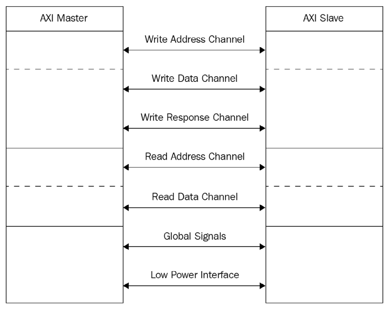
Figure 3.7 – AXI bus multi-channel topology
AXI bus global signals
The following diagram illustrates the connectivity of the global signals:

Figure 3.8 – AXI bus global signals connectivity
AXI write address channel signals
The following diagram illustrates the connectivity of the AXI write address channel signals:
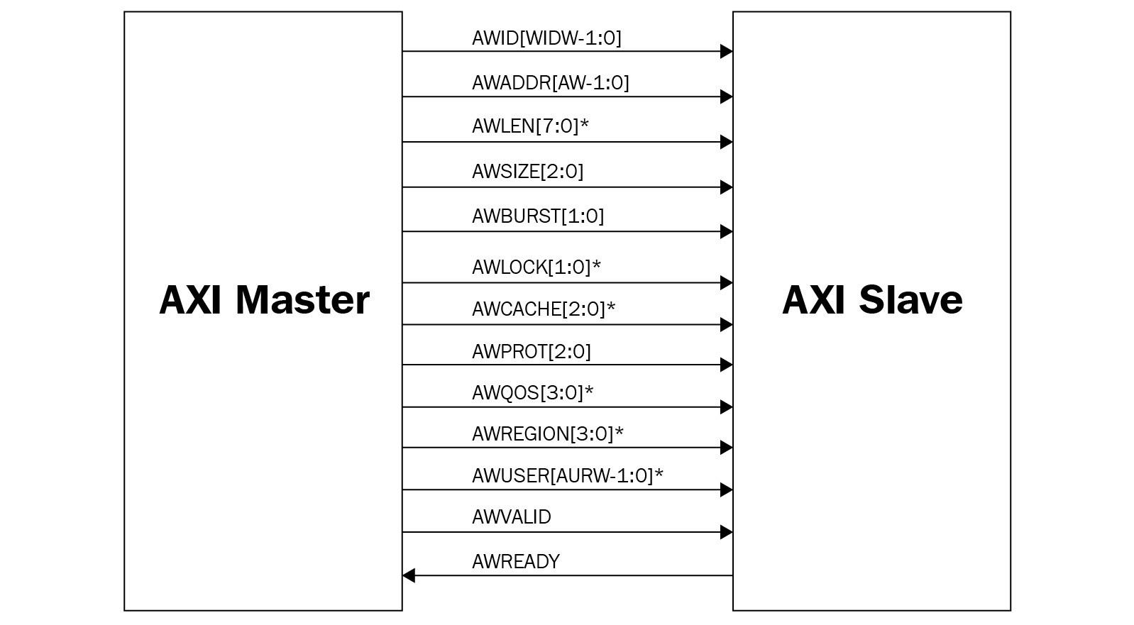
Figure 3.9 – AXI bus write address channel signals connectivity
Signals with an asterisk (*) next to them mean that they present differences between AXI-3 and AXI-4.
AXI write data channel signals
The following diagram illustrates the connectivity of the AXI write data channel signals:

Figure 3.10 – AXI bus write data channel signals connectivity
Signals with an asterisk (*) next to them mean that they present differences between AXI-3 and AXI-4.
AXI write response channel signals
The following diagram illustrates the connectivity of the AXI write response channel signals:

Figure 3.11 – AXI bus write response channel signals connectivity
Signals with an asterisk (*) next to them mean that they present differences between AXI-3 and AXI-4.
AXI read address channel signals
The following diagram illustrates the connectivity of the AXI read address channel signals:

Figure 3.12 – AXI read address channel signals connectivity
Signals with an asterisk (*) next to them mean that they present differences between AXI-3 and AXI-4.
AXI read data channel signals
The following diagram illustrates the connectivity of the AXI read data channel signals:

Figure 3.13 – AXI bus read data channel signals connectivity
Signals with an asterisk (*) next to them mean that they present differences between AXI-3 and AXI-4.
AXI low-power interface signals
The following diagram illustrates the connectivity of the AXI low power interface signals:

Figure 3.14 – AXI low-power interface signals connectivity
AXI bus-supported transactions
An AXI transaction is initiated by an AXI master toward an AXI slave performing either a read operation, a write operation, or a user-defined operation. The payload data is moved over the AXI bus using an AXI burst, which is formed by AXI beats. Three types of burst transfers are supported: FIXED (0b00), INCR (0b01), and WRAP (0b10), as specified by the AxBURST[1:0] vector (x being R for the read transactions and W for the write transactions). AxLEN[7:0] (x being R for read and W for write) specifies the burst length, which can be 1 to 16 transfers in AXI-3 for all burst types. It is 1 to 16 transfers in AXI-4 for the FIXED and WRAP bursts, though the INCR burst can be from 1 to 256 transfers for AXI-4. In addition to the size and layout, some attributes are associated with transactions, as defined by the AxCACHE[3:0] vector (x being R for read and W for write). This vector helps in qualifying the memory and peripheral slave support and, as such, how the system handles them while progressing through interconnects and bridges. It also specifies how the system-level caches deal with them when involved.
The AXI protocol also supports protection via the AxPROT[2:0] vector (x being R for read and W for write) in a similar mapping to the PPROT[2:0] in the APB protocol:
- AxPROT[0]: Indicates if this is a normal or privileged transaction and usually reflects the status of the running state of the Requester. It can easily be mapped by the CPU to its execution state (kernel mode or user mode, for example).
- AxPROT[1]: secure or non-secure. This signal can be used to implement hardware security by allowing access to certain registers when the transaction is classified as secure – that is, PPROT[1] is LOW. When PPROT[1] is set to HIGH by the Requester, access to secure registers, for example, is prohibited by the Completer.
- AxPROT[2]: Data or instruction. This signal provides a hint regarding the type of data exchanged by the transaction.
The AXI protocol adds the possibility of transaction processing and progressing concurrency if they are not tagged with the same AXI ID. All transactions from the same master that have been tagged with the same AXI ID must be processed by the slave and sent back to the issuing master in the same order they first arrived. However, transactions from the same master toward the same slave and with different AXI IDs can be processed and completed out of their arriving order. This property allows for better system performance if progress can be made outside of the processing ordering rule.
More Information
For a detailed description of the AXI transaction characteristics, you are encouraged to study the AXI-4 and AXI-3 protocol specifications, which are available at https://developer.arm.com/documentation/ihi0022/hc/?lang=en.
AXI bus example system implementation
A good example of using AXI-3 as the main bus protocol of an SoC can be seen in the following Zynq-7000 SoC interconnect diagram. The control path uses the APB bus to control peripheral registers and check the IP status at runtime. Memory and high throughput peripheral paths are implemented using the AXI-3 bus and its interconnects:
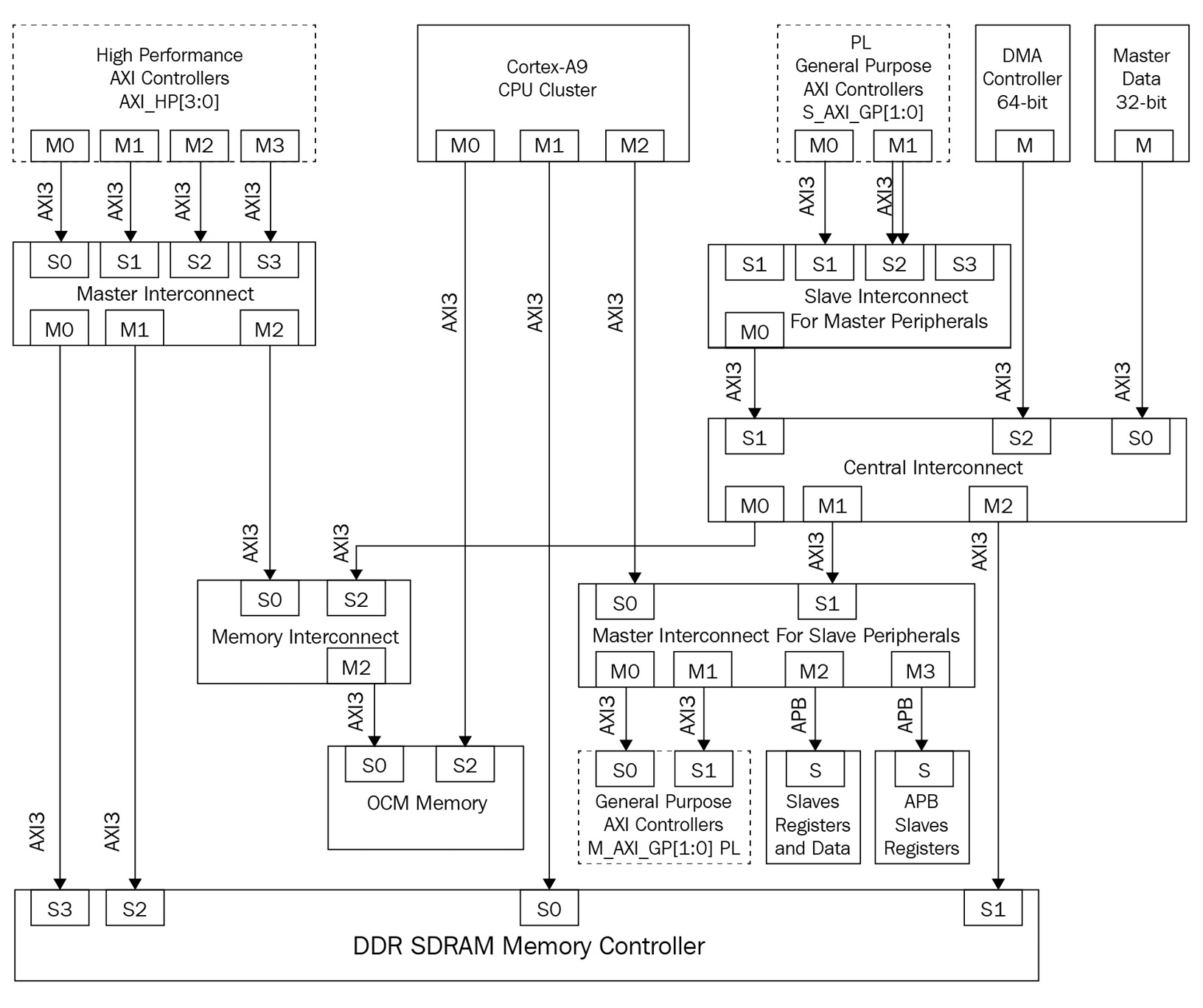
Figure 3.15 – AXI interconnect-based system example – the Zynq-7000 SoC
AXI Stream bus protocol overview
The AXI Stream bus protocol was first introduced by ARM in AMBA4. It is a serial point-to-point link that connects two IPs for data and control information exchange. This section will explore the AXI Stream bus protocol, its evolution from AMBA4 to AMBA5 standards, and its added features and mechanisms. We will understand this bus’s supported transactions, signaling, and application use cases. We will provide an example system implementation using the AXI Stream bus.
AXI Stream bus protocol evolution
At the time of writing, AXI Stream in the AMBA5 standard is at its second revision. The first revision appeared in AMBA4 as a way to connect two IPs to exchange data in a single direction – that is, one interface acting as a master and the other interface acting as a slave. AXI Stream in AMBA5 added two main features: wake-up signaling and parity protection. To build bidirectional data exchange mechanisms between two IPs, two AXI Stream buses can be used by deploying one in each direction. An AXI Stream bus can cross an interconnect, but often only for data width adaptation, such as upsizing or downsizing. It can also perform clock domain crossing when the master and the slave clocks belong to two different clock domains.
AXI Stream bus characteristics
The AXI Stream protocol defines three types of bytes: a data byte, which is the information to be transferred from a master interface to a slave interface, a position byte, which indicates the relative positions of data bytes in a stream of data, and a null byte, which is not a data nor a position byte. These bytes are qualified by the TKEEP and TSTRB signals on the AXI Stream bus, as indicated by Table 3.4, where the slave can discard null bytes and use position bytes to format the data transfer sequences or implement a higher custom protocol transparently on the underlying AXI Stream bus protocol.
AXI Stream also defines a transfer to exchange data through the AXI Stream interface. This is done within a TVALID and TREADY handshake between the master and slave interfaces. A packet contains several data bytes that belong to the same transfer or transfers, similar to a burst transaction in the AXI-4 bus protocol. A frame is a logical grouping of multiple packets with each assembling several data bytes. A data stream is used to transfer data from a master to a slave as many individual byte transfers or as a grouping of packets. The AXI Stream protocol supports three types of handshake sequences between the master and the slave:
- Handshake with TVALID, as asserted by the master before TREADY is asserted by the slave.
- Handshake with TVALID, as asserted by the master after TREADY is asserted by the slave.
- Handshake with TVALID and TREADY, asserted concurrently.
AXI Stream bus interface signals
This section summarizes the signals that form the AXI Stream bus interface for both the master and the slave. Taking a closer look at these signals will provide a good overview of the protocol mechanics to move data from source to destination. However, you are encouraged to examine the protocol specification from ARM at https://developer.arm.com/documentation/ihi0051/b/?lang=en.
The following table lists the AXI Stream bus interface signals:
|
Signal |
Width |
Description |
|
ACLK |
1 |
Interface clock signal that’s used for sampling all the bus signals on the rising edge. |
|
ARESETn |
1 |
Interface global reset, active low. |
|
TVALID |
1 |
A master interface signal indicating that data is valid on the TDATA lane. |
|
TREADY |
1 |
A slave interface signal indicating that the slave is ready to accept the data on the TDATA lane. |
|
TDATA |
TDW |
The bus data lane’s size, which can be 8, 16, 32, 64, 128, 256, 512, or 1,024 bits. |
|
TSTRB |
DW/8 |
A byte qualifier indicating that the associated byte in the TDATA lane is a data byte or position byte type. |
|
TKEEP |
DW/8 |
A byte qualifier indicating that the associated byte in the TDATA lane is a data/position byte or a null type. This indicates if the associated byte needs processing at all. |
|
TLAST |
1 |
Packet delimiter. |
|
TID |
TIDW |
Used as a data stream ID with TIDW <= 8. |
|
TDEST |
TDESW |
Helps route the data stream through AXI Stream topologies that have multiple hopes in their paths. TDESW <= 8. |
|
TUSER |
TUW |
Sideband information that’s used to extend the AXI Stream protocol by the user. |
|
TWAKEUP |
1 |
Part of the AXI-5 Stream protocol that’s used to indicate that there is activity in the AXI-5 Stream bus. |
Table 3.4 – AXI Stream bus interface signals description
AXI Stream bus-supported transactions
The AXI Stream protocol defines four styles of data streams: the byte stream, the continuous aligned stream, the continuous unaligned stream, and the sparse stream. Let’s look at each in detail.
Byte stream style
In a byte stream transfer style, all the byte types can be used. The following diagram illustrates a byte-stream transfer, where the interface is 4 bytes wide:

Figure 3.16 – AXI Stream protocol byte stream example
In the preceding diagram, Word 0 is the first four bytes to be transferred across the bus from the master to the slave and it has B00, B01, and two null bytes forming it. This is followed by Word 1, Word 2, and so on.
Continuous aligned stream style
In a continuous aligned stream, only the data byte type can be used. The following diagram shows a continuous aligned stream transfer, where the interface is 4 bytes wide:

Figure 3.17 – AXI Stream protocol continuous aligned stream style example
In the preceding diagram, Word 0 is the first four bytes to be transferred across the bus from the master to the slave and it has B00, B01, B02, and B03 bytes in it. This is followed by Word 1, Word 2, and so on.
Continuous unaligned stream style
In a continuous unaligned stream, only the data byte and position types can be used, with the condition that position bytes can only be used at the beginning of a data packet, at the end of a data packet, or on both. The following diagram shows a continuous unaligned stream transfer, where the interface is 4 bytes wide:

Figure 3.18 – AXI Stream protocol continuous unaligned stream style example
In the preceding diagram, Word 0 is the first four bytes to be transferred across the bus from the master to the slave and it has B00, B01, B02, and B03 bytes in it. This is followed by Word 1, Word 2, and so on. The first packet has a two-byte position type at the end, whereas the second packet has the byte position bytes type both at the beginning and the end of the packet.
Sparse stream style
In a sparse stream, there are data byte and position byte types. The pattern of the data bytes and position bytes should be the same in all packets. The following diagram shows a sparse stream transfer, where the interface is 4 bytes wide:

Figure 3.19 – AXI Stream protocol sparse stream style example
AXI Stream bus example system implementation
The AXI Stream bus is used in many designs to solve the issue of having to go through the main system interconnect to exchange data or control information between two specific IPs. For example, the ARM GIC-600 interrupt controller uses the AXI Stream bus to distribute interrupts from the GIC-600 to the CPU cluster, such as the ARM Cortex-73. The following diagram illustrates this connectivity:
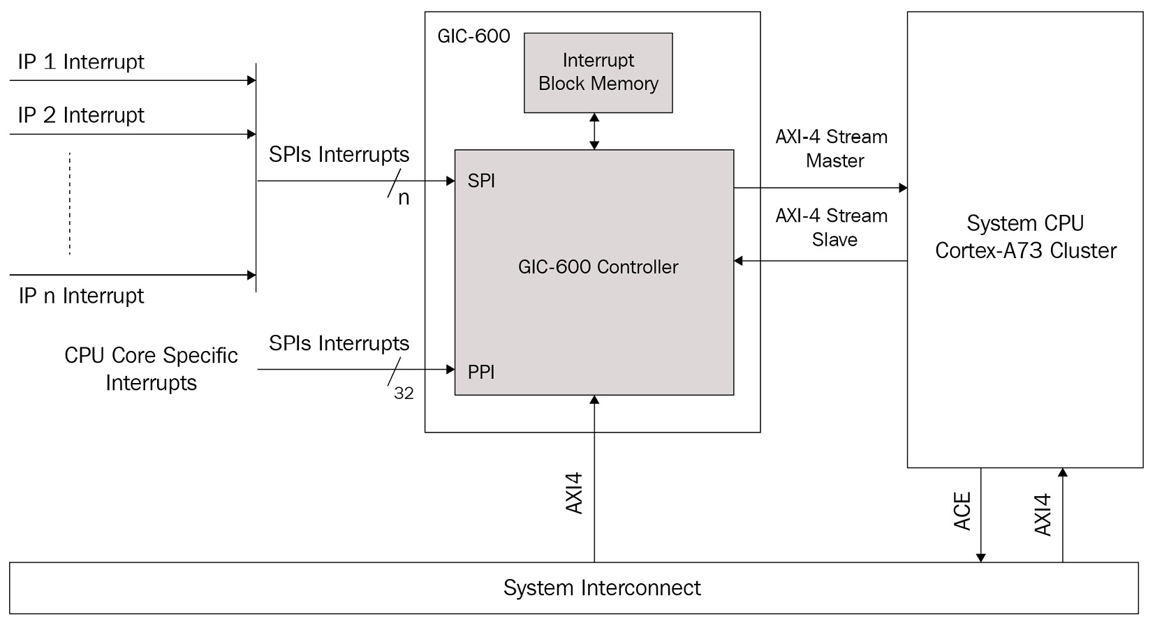
Figure 3.20 – System example of using the AXI stream bus – the ARM GIC-600
ACE bus protocol overview
The ACE bus protocol, also known as AXI with Coherency Extensions, was first introduced by ARM in AMBA4. It is an AXI-4 protocol with support for cache coherency that’s implemented in hardware between different masters, including caches. This section provides an overview of the system cache coherency concepts that will be covered in more detail in the last section of this chapter. We will also explore the ACE protocol, its evolution from AMBA4 to AMBA5 standards, and its added features and mechanisms. We will understand this bus’s supported transactions, signaling, and application use cases. We will provide an example system implementation that uses ACE as a bus interface.
ACE bus protocol evolution
The ACE bus protocol is in its second revision as part of the AMBA5 standard. It was first released in AMBA4 as a means to connect masters that include caches and allow the data exchanges to be cache coherent without any software cache maintenance operations. Performing these cache maintenance operations by the hardware interconnecting these masters provides an advantage in terms of processing performance and flexibility in parallel processing software architectures. This is because it makes lock-free programming easier to implement in multi-core and multiprocessor SoCs. In the ACE protocol, a cache line can be in one of the five states supported under ACE. Each state has an associated action when it is accessed under ACE. This extra information and actions require an extra set of signals and channels to extend the AXI-4 protocol to evolve and become an ACE protocol. It also adds support for barrier transactions to enforce transaction completions ordering in the interconnect, as well as support for Distributed Virtual Memory (DVM) to manage virtual memory addressing at the interconnect level. It extends it to the outside of a specific CPU cluster. AMBA5 standard reorganized the ACE protocol by defining three Lite versions: ACE5-Lite, ACE5-LiteDVM, and ACE5-LiteACP. Barrier transactions support was removed from ACE5 and ACE5-Lite. AMBA5 also removed all references to the low power interface in prior standards as it is now grouped under another protocol, known as the AMBA Low Power Interface specification. In this book, we will focus more on the ACE base protocol, ACE-4, as it is used within the Xilinx Zynq UltraScale+ SoC devices. These are part of the SoCs we will build projects for in the third part of this book.
ACE bus characteristics
As mentioned previously, the ACE protocol is AXI-4 at the base of the specification and provides cache coherency hardware support, which is defined between masters. It also includes and uses the caches of shared memories among them. ACE-4 allows writes to be made to the same memory address by two different masters. These are to be viewed in the same order by all the observing masters that share the same address location of the memory. The ACE-4 protocol implements system-level coherency, where the design can specify the ranges of coherent memories, the memory controllers that support the coherency extensions, and how software can communicate between the elements of the system coherency domain. ACE-4 also provides an abstraction protocol that allows coherency to be implemented between caches that use different coherency protocols. We will introduce coherency protocols in detail in the last section of this chapter. It also allows IPs with different cache line characteristics such as granularity to interoperate coherently. The following diagram provides a simple abstracted example of an ACE-4-based SoC, which should help us study its characteristics:

Figure 3.21 – ACE-4 based interconnect simple system example
Cached copies of data from the shared system memory are mapped to all the four master’s address spaces as cacheable regions. These can reside in any of the five states in any local cache of one or more master IPs participating in the SoC coherency domain. ACE-4 guarantees that all the masters in the SoC have visibility of the latest value with the data stored in the memory location. This is done by enforcing that only one copy exists (in all the local masters’ caches and the system memory) whenever a write operation targets that shared memory location. Once the write operation to the shared memory location is complete, all the participating masters will obtain the latest copy of the data held in the memory location that was targeted by the last write operation. This mechanism allows multiple copies of the data, stored in the shared system memory location as coherent, to exist in multiple locations throughout the caches and the system memory at the same time. As in any efficient coherency protocol, ACE-4 does not require an automatic and immediate write-back of recently updated data in a given cache to the system memory. This is only necessary when a memory location is no longer stored in a sharable cache as a result of an explicit software cache maintenance operation or a hardware speculative cache operation on its location, which is elected as a victim under the applied cache hardware manager algorithm. The ACE-4 protocol allows the master components to find out whether a cache line is unique to its cache or if it also exists in another master’s cache. In the case of uniqueness, the master can change the content of its cache line without broadcasting the change to all the other participating masters. If it isn’t unique, then the master must notify them.
The following table lists all the cache states defined in the ACE-4 protocol:
|
Cache State |
Description |
|
Invalid (I) |
The cache line is not present in this specific cache. |
|
UniqueClean (UC) |
The cache line is only present in this cache and it still matches the content of the memory location. This allows the owning master to write to this cache line without broadcasting the information to other masters in the system. |
|
UniqueDirty (UD) |
The cache line is only present in this cache, and it has been modified vis-a-vis the memory location, which allows the owning master to write to this cache line again without broadcasting the information to other masters in the system. |
|
SharedClean (SC) |
The cache line might be present in other caches. It is not known if it still matches the system’s memory. However, this master is not responsible for updating it in the system memory, so they must notify any other masters before writing to their cache line while in this state. |
|
SharedDirty (SD) |
The cache line might be present in other caches, and it has been modified vis-à-vis the system memory. This master is responsible for updating it in the system memory and must notify any other masters before writing to their cache line while in this state. |
Table 3.5 – ACE-4 protocol cache line states description
The ACE-4 protocol states the following rules regarding the cache line states:
- A cache line that is in a unique state can only be resident in one cache in the entire SoC.
- A cache line must be held in a shared state as soon as it is present in more than one cache in the SoC.
- A cache that obtains a new copy of a cache line causes another cache holding the same cache line copy in a unique state to become shared.
- When a cache evicts a cache line, there’s no need to inform other cache line holders. This could cause a shared cache line state to only be in one cache.
- A cache line that has been changed vis-à-vis the system memory. It should be in a dirty state.
- A cache line that has been changed vis-à-vis the system memory and is in more than one cache in the SoC should be in a dirty state in only a single cache.
ACE bus interface signals
ACE-4 modifies the read address, write address, and read data channels of AXI-4 by adding the signals listed in the following table. The write data and write response channels are the same in both AXI-4 and ACE-4:
|
AXI-4 Channel |
Added Signal |
Description |
|
Read address |
ARDOMAIN[1:0] |
Driven by the master interface, this indicates the shareability domain of a read transaction as being either Non-Shareable (0b00), Inner Shareable (0b01), Outer Shareable (0b10), or System (0b11). |
|
ARSNOOP[3:0] |
Driven by the master interface, this indicates the read transaction type. There are five groups of transaction types: Non-snooping, Coherent, Cache maintenance, Barrier, and DVM. Each group defines many read transaction types. | |
|
ARBAR[1:0] |
Driven by the master interface, this defines the barrier transactions for the read address channel as Normal access, respecting barriers (0b00), Memory barrier (0b01), Normal access, ignoring barriers (0b10), or Synchronization barrier (0b11). | |
|
Write address |
AWDOMAIN[1:0] |
Driven by the master interface, this indicates the shareability domain of a write transaction as being either Non-Shareable, Inner Shareable, Outer Shareable, or System. |
|
AWSNOOP[2:0] |
Driven by the master interface, this indicates the write transaction type. There are four groups of transaction types: Non-snooping, Coherent, Cache maintenance, and Barrier. Each group defines many write transaction types. | |
|
AWBAR[1:0] |
Driven by the master interface, this defines the barrier transactions for the write address channel as Normal access, respecting barriers (0b00), Memory barrier (0b01), Normal access, ignoring barriers (0b10), or Synchronization barrier (0b11). | |
|
AWUNIQUE |
Driven by the master interface, this is only required by IPs that support WriteEvict-type transactions. | |
|
Read data |
RRESP[3:2] |
Driven by the slave interface, this extends the AXI-4 read response by two bits to provide the Shareable read transaction completion information. RRESP[2] is defined as the PassDirty bit, while RRESP[3] is defined as IsShared. |
Table 3.6 – ACE-4 channels based on the AXI-4 channels description
ACE-4 adds three extra channels to the AXI-4 channels, which are the snoop address channel, the snoop response channel, and the snoop data channel. The snoop address channel provides the value of the snooped address, as well as the associated control information. The snoop response channel is a way for the snooped master to complete the snoop address request and it indicates if a data transfer is going to follow on the snoop data channel. The following table provides an overview of the snoop channel topology:
|
ACE-4 Channel |
Added Signal |
Description |
|
Snoop address |
ACVALID |
Driven by the slave interface, this indicates that the values on the snoop address and the control signals are valid. |
|
ACREADY |
Driven by the master interface, this indicates that the snoop address and control signals can be accepted within the current clock cycle. | |
|
ACADDR[ac-1:0] |
Driven by the slave interface, this is the snooped address. Its width should be the same as the read and write address channels. | |
|
ACSNOOP[3:0] |
Driven by the slave interface, this indicates the snoop transaction type. | |
|
ACPROT[2:0] |
Driven by the slave interface, this indicates the security level of the snoop transaction. Only ACPROT[1] has a meaning in the snoop channel. | |
|
Snoop response |
CRVALID |
Driven by the master interface, this indicates that the snoop response from the master is valid. |
|
CRREADY |
Driven by the slave interface, this indicates that the interconnect is ready to accept the snoop response from the master. | |
|
CRRESP[4:0] |
Driven by the master interface, this indicates the snoop transaction’s response. | |
|
Snoop data |
CDVALID |
Driven by the master interface, this indicates the validity of the snoop data back from the master. |
|
CDREADY |
Driven by the slave interface, this indicates that the interconnect slave interface is ready to accept the response data from the master. | |
|
CDDATA[cd-1:0] |
This is driven by the master interface and indicates the snoop data that’s gone from a master back to the interconnect. “cd” is the width of the snoop data bus. | |
|
CDLAST |
This is driven by the master interface and indicates the snoop data transaction’s last transfer. |
Table 3.7 – ACE-4 specific snoop channels description
ACE bus-supported transactions
ACE-4 protocol defines seven types of transactions:
- Non-snooping transactions: These are used to access locations in the address space that are defined as non-shareable or device – that is, they can’t be in another master’s cache. To gain access to these locations, the master can use ReadNoSnoop or WriteNoSnoop.
- Coherent transactions: These are used to perform coherent access via a vis other master caches – that is, the accessed locations are shareable locations that can potentially reside in the cache of another coherent master in the SoC. To read data from a coherent cache line, the master can issue ReadClean, ReadNotSharedDirty, and ReadShared. To perform a write transaction to shareable locations, a coherent master can use ReadUnique, CleanUnique, and MakeUnique. To write to shareable locations when no cached copy is required, the master can use ReadOnce, WriteUnique, and WriteLineUnique.
- Memory update transactions: To update the system memory, the master can use the WriteBack transaction to write back a dirty line of the cache to memory and free it. However, to retain a copy of the cache line, the master should issue a WriteClean transaction. A WriteEvict transaction can be used in a multi-layer cache hierarchy to free a cache line and write it into a lower cache level without updating the system memory. Evict is used to broadcast the address in a cache line of a master to other masters without writing any data back to the system memory.
- Cache maintenance transactions: These are used by masters in a coherency domain to broadcast cache operations to access and maintain the caches of other coherent masters in the coherency domain. The cache maintenance transactions are CleanShared, CleanInvalid, and MakeInvalid.
- Snoop transactions: These use the snoop address, snoop response, and snoop data channels. Snoop transactions are a subset of coherent transactions and cache maintenance transactions.
- Barrier transactions: These are used to implement the transactions ordering rule. ACE-4 supports the memory barrier and synchronization barrier types.
- Distributed virtual memory transactions: These are used to maintain the system’s virtual memory and share information between the elements of the SoC participating in its implementation. It usually includes a System Memory Management Unit (SMMU).
The ACE-4 coherency extension is a complex topic on its own. This section has only provided an overview of it and how its addition makes coherency possible between different participating masters. You are encouraged to consult the ARM ACE-4 specification for more details: https://developer.arm.com/documentation/ihi0022/e?_ga=2.67820049.1631882347.1556009271-151447318.1544783517.
ACE bus example system implementation
A good example of using the ACE-4 protocol as the main bus protocol of an SoC is illustrated by the Zynq UltraScale+ SoC interconnect of the APU unit. It includes a Cache Coherent Interconnect (CCI) and an SMMU:
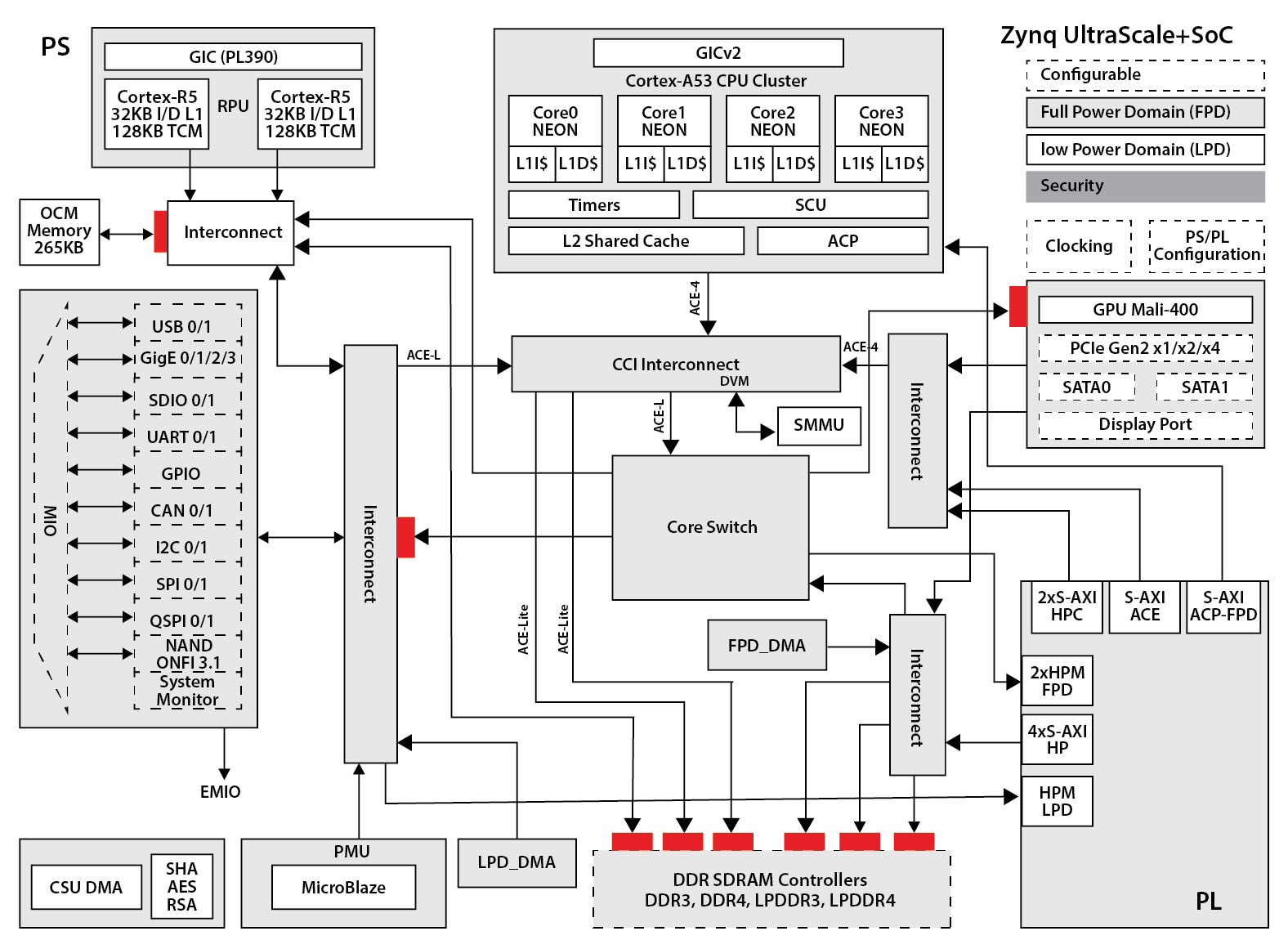
Figure 3.22 – ACE-4 based interconnect system implementation example
OCP interconnect protocol
OCP is an industry standard that provides the specification of a socket-based bus interface that can be used in an interconnect for modern SoCs. It is developed and maintained by the OCP Working Group. The OCP specification is available from Accellera for free and requires the user to accept the Accellera OCP Specification License. Other materials that are provided with the OCP protocol can be found under the Apache 2.0 license. To download the OCP specification, go to https://www.accellera.org/downloads/standards/ocp/ocp-license-agreement.
This section only provides a brief introduction to the OCP protocol so that you can gain a high-level understanding of its mechanics and characteristics, as well as compare it to AMBA-based bus protocols such as AXI-4 or ACE-4. However, you are encouraged to study the relevant sections of the specification to further your knowledge of the protocol and its implementation details.
OCP protocol overview
The OCP protocol is a high throughput and high-speed IP interface. It can be implemented in systems that use an SoC interconnect that is not based on the OCP protocol, so long as bridging is performed correctly to and from the OCP interfaces. It helps in overcoming the time-to-market challenges in the SoC’s design by providing an industry-standard bus protocol that can cohabit easily with other SoC bus protocols and system interconnects. The OCP protocol is flexible as it can be configured to tailor to the system’s design needs. Here, the user can choose the options that are needed and discard the features that aren’t specified in their design. This makes it an extensible bus protocol in concept, which also helps in reducing the silicon area cost when using it as an IP bus interfacing protocol. In addition to supporting the Virtual Component Interface (VCI), the OCP protocol includes the sideband control signals and the test signals. The VCI is specified by the Virtual Socket Interface Alliance (VSIA).
At the time of writing, the current revision of the OCP protocol is revision 3.0, which added coherence extensions to the base protocol, new sideband signals to control the IP connection state of the interface, and an advanced high-speed profile.
OCP bus characteristics
The OCP protocol is a point-to-point connection between two IP cores, with one acting as a master and the other as a slave. Communication is initiated by the master and the slave completes it by accepting the write data from the master or responding with the read data requested by the master in the command. For a data exchange to occur between the two communicating IPs, the master puts the command, the control information, and data in a write scenario on the OCP bus. This goes through an interface block that acts as a slave on the SoC interconnect, which may bridge it to another protocol if the SoC interconnect uses a different one. Then, the end target receives the initial command and the associated information and potential write data. The OCP protocol is flexible and provides a synchronous handshaking signal that allows a pipelined or multi-cycle access model to be used between the master and the slave. It is also worth noting that the OCP protocol is connection-oriented, which is why it’s called a socket interface. Here, the IP can connect and disconnect from the bus infrastructure if the SoC interconnect supports this feature.
OCP bus interface signals
OCP interface signals are divided into three categories: dataflow signals, sideband signals, and test signals.
There are three functional sets within the dataflow signals: the request signals set, the response signals set, and the data handshake set. The dataflow signals can also be divided into five groups: basic signals, simple extensions, burst extensions, tag extensions, and thread extensions.
Only a few basic dataflow group signals are mandatory for an OCP interface configuration. The optional signals can be used to support the need for the communicating OCP interface. The sideband and test signals are all optional. The OCP has a single clock to which all the interface signals are synchronized. The following diagram illustrates the OCP interface signals grouping:

Figure 3.23 – OCP interface signals grouping
For details of all the signals that form the OCP bus, please consult the OCP specification at https://www.accellera.org/downloads/standards/ocp/ocp-license-agreement.
OCP bus-supported transactions
The following diagram shows the OCP protocol’s layout and how it is implemented using the predefined groups and sets of signals:
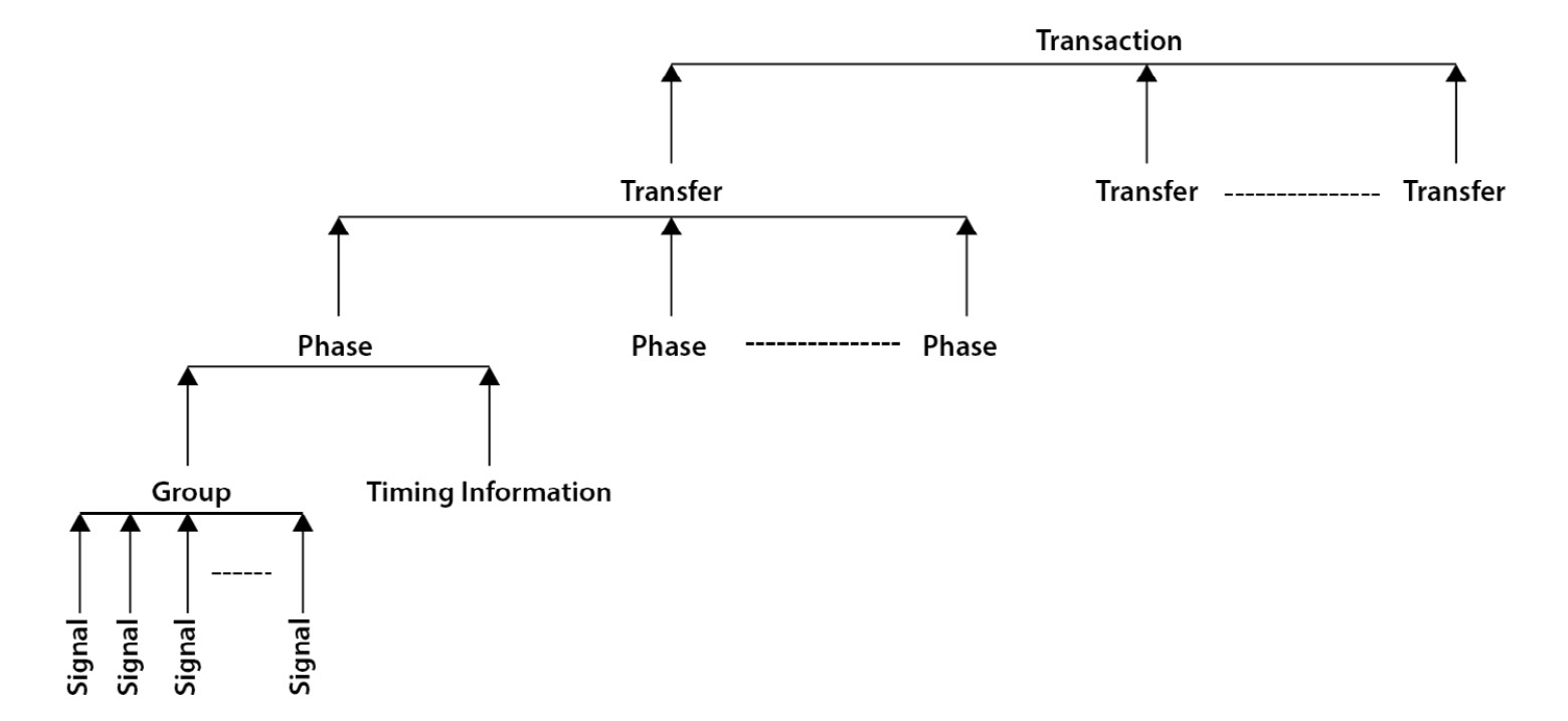
Figure 3.24 – OCP protocol elements hierarchical representation
The transfer commands indicate the types of OCP transactions. These are encoded in the MCmd[2:0] signal, which is part of the request group of signals, as follows:
- 0b000: Idle.
- 0b001: Write transfers the data from the master to the slave.
- 0b010: Read requests the data by the master from the slave.
- 0b011: ReadEx is paired with a Write or WriteNonPost and has a blocking effect.
- 0b100: ReadLinked is used with WriteConditional and has no blocking effect.
- 0b101: WriteNonPost is used to request the slave not to post a Write command.
- 0b110: WriteConditional is used to write only when there is a reservation on the write address set. If not, it fails.
- 0b111: Broadcast is used when the addressed location may map to more than one slave.
ReadExclusive, ReadLinked, and WriteConditional have similar effects on some processor semantics that are used to synchronize multiple CPU cores in an SoC.
The OCP protocol also supports burst operations to achieve high system throughput with minimum overhead. OCP burst operations may include addressing details for each transfer command or just one for the full burst transfer.
The OCP protocol uses tags to relax operation ordering that belongs to the same master, so operations with different tags may be treated with a relaxed ordering in the completion phase by the slave.
DMA engines and data movements
Modern SoCs and high-performance IPs include DMA engines to offload data movement from the CPUs and perform it as desired by the software, with the option to notify the CPU once the operation is completed. There are two categories of DMA engines: DMA engines that are included within an IP, and central DMAs that are standalone and connected to the SoC interconnect like any other SoC IP.
IP-integrated DMA engines overview
IP-integrated DMA engines act as data movers on behalf of the IP and the CPU, so the CPU won’t be needed to copy data from system memory to the IP’s local storage or vice versa. Rather, when programmed and armed, once the data is needed or received, the DMA engine autonomously performs the data transfer from source to destination. Then, its control hardware notifies the CPU when the operation has finished executing, usually via an interrupt. The following diagram illustrates an IP-integrated DMA engine:

Figure 3.25 – IP-integrated DMA engine example
IP-integrated DMA engines topology and operations
Most high-speed IPs include a DMA engine that has multi-channels. They are also full-duplex so that data movement isn’t the SoC bottleneck for meeting system performance requirements. The topology of the DMA engine to include many channels that are capable of reading and writing simultaneously is to be able to service the data movement needs of the IP itself. High-performance communication IPs, such as the PCIe controllers and the multi-gigabit Ethernet controllers, can move a high quantity of data in both the transmit and receive directions. They usually service many software threads running on different CPU cores. These use case scenarios require an efficient and low overhead data movement within the SoC between the system memory and these controllers. The integrated DMA engines within these controllers are the appropriate solution to meet these needs.
Integrated DMA engines, in contrast to central DMA engines, have the advantage of moving the data directly from system memory to the controller or vice versa. Consequently, the data reaches its destination in half the required time it may need when using a central DMA engine, where data needs to be copied to the central DMA engine buffer from the source, then written out to the destination.
IP-integrated DMA engines are capable of moving data from/to regular memory with sequential addressing and from/to peripherals (where a FIFO is usually used as storage) and the address of the source or destination is the same. To support peripherals with integrated FIFOs (and if not managed by the IP peripheral itself behind a bus interface), some integrated DMA engines use handshaking signals to manage the communication directly with the FIFO. These DMA engines aren’t generic and are usually designed to support a specific hardware interface. Moving data from regular memory is generic in the sense that the DMA engine will interface to the system interconnect via, for example, one of the covered AMBA or OCP bus protocols and then perform the operations using these bus protocols.
The data movements to be performed are seen as operations that are executed by the DMA engine. These operations are performed by the DMA hardware state machine using operands that are specified via registers local to the DMA engine. This set of operands is called the DMA operation descriptor. Among the required operands in a DMA descriptor for a read/write from/to system memory where the data is stored/to be written in a contiguous physical buffer, we can find the following:
- The source/destination address of the data
- The size of the data transfer
- Control information
- Start/stop
The DMA engine then stores the results of the operation, such as a progress watermark, error status, and completion status, in a set of registers that software can read when appropriate.
There are also DMA engines capable of transferring complex structures of the data from the system memory to its local storage without any data rearrangements. These complex data structures are usually data buffers scattered around physical buffers of different sizes in the system memory. Some DMA engines can perform such transfers using a linked list of the aforementioned DMA descriptors, where the DMA engine will read them in the execution stage sequentially. Once the executed list reaches the last entry, it will point to the next list. This list is usually a contiguous number of descriptors; however, the last element of the list is just a pointer to the next list of descriptors. This result in the software needing to define the linked list of descriptors in the system memory, and then provide the address of the first element of the linked list of descriptors to the DMA engine to load before launching the DMA operation. The process of loading the linked list of DMA descriptors is often called pre-fetching as it is an operation that’s performed while a DMA operation of a previous sequence is ongoing. The operands for such DMA operations are as follows:
- The type of the descriptor is a data buffer descriptor or a pointer to the first element of the next linked list.
- The source address of the data is a data buffer or the location of the next first element of the next list.
- The size of the data to transfer if it’s not a pointer.
- Control information.
- Start/stop.
Every IP-integrated DMA engine may have a specific way of implementing this to interface with the software, but the general concept is pretty much the same. The following diagram illustrates the DMA descriptors linked list concept:

Figure 3.26 – IP integrated DMA descriptors linked list example
Standalone DMA engines overview
Standalone DMA engines are often called central DMAs as they are central in the SoC interconnect and can move data from anywhere in the SoC-mapped address space to anywhere else, as far as they are allowed to do so by the SoC interconnect and any security policy that may restrict access to some regions of the address space.
Like the IP integrated DMA engine, a central DMA IP autonomously performs the data transfer from source to destination. It control hardware proceeds to notify the CPU via an interrupt once the required transfer operation has finished. The following diagram illustrates the notion of central DMA engines:

Figure 3.27 – Central DMA engine example
Central DMA engines topology and operations
Most modern SoCs include a central DMA engine with multi-channels that are full-duplex to accelerate the data moving operations on behalf of the CPU and IP peripherals that have no integrated DMA engine. There are many topologies of the central DMA engines that vary in design complexity and features, as well as silicon area cost. However, usually, central DMA engines include multiple channels capable of concurrent read and write transfers from different sources and destinations either by sharing their master interface or by implementing multiple masters.
Central DMA engines, as already mentioned and in contrast to IP integrated DMA engines, need to copy the data from the source to the central DMA buffer, then copy the data from the central DMA buffer to the destination. Consequently, the data reaches its destination in twice the required time it may need when using an IP-integrated DMA engine, where data is transferred directly from the IP to the destination or vice versa.
A central DMA engine can move data between different types of sources and destinations, as follows:
- Memory to memory
- Memory to FIFO
- FIFO to memory
- FIFO to FIFO
- Scatter Gather (SG)
A Scatter Gather DMA operation is a specific type of data transfer from memory to memory where the source of the data and its destination is formed by non-contiguous buffers in the physical memory address space.
Similar to an integrated DMA engine, the data movements to perform are seen as operations that are executed by the central DMA engine. These operations are performed by the DMA hardware state machine using operands that are specified via registers local to the DMA engine. This set of operands is called the DMA operation descriptor. Among the required operands in a DMA descriptor for a read/write from/to system memory where the data is stored/to be written in a contiguous physical buffer, we can find the following:
- The source address of the data
- The destination addresses of the data
- The size of the data transfer
- Control information
- Start/stop
Then, the central DMA engine stores the results of the operation, such as a progress watermark, error status, or completion status, in a set of registers that software can read when appropriate.
Like the IP-integrated DMA, central DMA engines are also capable of moving complex data structures from source to destination using the linked list of DMA descriptors concept explained in the previous section.
Data sharing and coherency challenges
Modern SoCs are constructed using multiple data compute engines such as CPUs, GPUs, custom hardware accelerators, and high-performance IP peripherals with integrated DMA engines. They process data that is shared laterally and passed from layer to layer as these different processing engines cooperate. These complex topologies make the system design more challenging in terms of making sure that the data is safe as it is accessed, used, and updated while also ensuring it is coherent when these processing engines make efforts to optimize the data access, such as by using integrated caches. Accessing data concurrently and safely means accessing it atomically and coherently without paying a high penalty in terms of software management and using prohibitive locking mechanisms. We want the system architecture to be lock-free and rely on the hardware to provide the optimal mechanisms to implement these data protection mechanisms.
Data access atomicity
To make sure that the data is accessed atomically in an SoC with multi compute nodes sharing it, the SoC system architecture should provide exclusive access primitives that cooperating compute elements can use to protect access to shared data. The atom of data access is specific to the application and can be a simple data type, such as an integer, or a custom-defined data structure that the application software wants to be accessible fully or partially to a single requester at a time. Traditionally, hardware-based primitives were used, such as hardware mutexes, and these can still be used in today’s SoCs. ARM also defines a whole end-to-end paradigm – that is, from the software layer to the local exclusive monitors within the cluster and the global exclusive monitors within the system memory controllers. These monitors are hardware-based state machines are implemented at the bus interface level of the CPU cluster for the local exclusive monitors or the bus side interface of the memory controller for the global exclusive monitors. They observe access sequences to memory locations where the semaphore-based primitives are located. This means that software threads can use these semaphores as a protective mechanism to access shared data between software threads running on the same CPU core, between software processes running on different CPU cores within the same CPU cluster, and between hardware or software threads running outside of a specific CPU cluster. Using hardware-based access protection primitives or exclusive (local and/or global) monitors is a choice that can be made based on the system’s sharing and performance requirements. System profiling should help with making the optimal choice, though using a mixture of both is usually the solution.
Information
If you wish to learn more about the global exclusive monitors topic, you are invited to study the ARM material at https://developer.arm.com/documentation/dht0008/a/arm-synchronization-primitives/exclusive-accesses/exclusive-monitors?lang=en.
Cache coherency overview
Cache coherency isn’t a new topic in the SoC design since it is the basis of building a multi-core cache-coherent CPU cluster. However, it now extends beyond the CPU cluster and reaches the SoC level via bus protocols such as ACE and OCP.
Cache coherency protocols overview
The following diagram illustrates the concept of sharing data between two CPUs and integrating caches in them. The shared data is cached from system memory. There is a need for a cache coherency protocol within the CPU cluster, a bus interface with coherency support such as ACE-4, and an interconnect with coherency support to allow these CPUs to share data coherently without costly (in terms of performance) software cache management being required:

Figure 3.28 – Cache coherency support infrastructure
If CPU1 modifies the content of the cache line that includes the 0xBABA_BABA location from system memory, then the Snoop Control Unit (SCU) will make sure that this access is done coherently since it has all the system coherency infrastructure to do so. Any CPU core from a CPU cluster can access shared data that is also cached coherently without the need to perform any software cache maintenance operations. This is because the hardware will take care of that autonomously.
Implementing cache coherency in CPUs
In a CPU cluster that’s integrating multiple cores, each with level 1 caches and at least another higher-level cache such as a common L2 cache, there is usually an SCU that orchestrates data accesses and makes sure that data is shared efficiently between the different CPU cores within the cluster, as well as shared coherently. The SCU implements a coherency protocol, which is usually a derivative of the MESI cache coherence protocol. Let’s look at what the MESI cache coherency protocol stands for:
- M: This stands for Modified and means that the cache line has been modified vis-à-vis the system memory.
- E: This stands for Exclusive and means that the cache line is exclusively present in the current cache.
- S: This stands for Shared and means that the cache line is present in at least another cache with this one.
- I: This stands for Invalid and means that the cache line is invalid.
Modified, Exclusive, Shared, and Invalid are four states under which, and at any time, a given cache line of any CPU core can be held. The modern multi-core CPU clusters have at least another state added to the MESI protocol to support useful cache coherency protocols, such as Owned. The protocol is called MOESI. Owned means that the cache controller where the cache line is in the Owned state and is responsible for updating the next-level cache or main memory.
With these five states, most of the cache controllers can, alongside the SCU, implement efficient cache coherency protocols and share data between the caches of the CPU cores within the cluster without having to go via memory. This reduces the data sharing latency, which, in turn, reduces power consumption by avoiding heavy bus and external memory traffic, thus augmenting system performance.
Extending cache coherency at the SoC level using the accelerators port
Some CPUs such as the ARM Cortex-R and Cortex-A have an Accelerator Coherency Port (ACP) that extends the cache’s coherency. The ACP helps in implementing an I/O-coherent topology that allows hardware accelerators and the CPU to share data coherently without software cache management assistance. However, this is only true in the I/O accelerator direction. This means that if the hardware accelerator integrates a cache, the CPU can’t access system memory that’s been cached within the hardware accelerator coherently. Therefore, it is important to understand how the ACP port operates in both the Cortex-A9 CPU cluster within the Zynq-7000 SoC and the ACP port of the Cortex-A53 CPU cluster of the Zynq UltraScale+ SoC.
When using the ACP port to extend I/O coherency with an accelerator, for example, care must be taken to ensure that the data access patterns and transaction types that are used by the accelerator master are supported by the ACP port. Not all the transactions that are supported by the bus protocol and used by the ACP port are permitted and there are limitations that the user needs to be aware of. These can be found in the CPU Technical Reference Manual (TRM).
When access is gained through the ACP, usually, if there is a hit in a CPU core cache, then the transaction is performed from the cache (be it read or write). However, if there is a cache miss, then the transaction is fulfilled from system memory, so there is a price to pay here in terms of added cycles of latency and performance sharing the CPU cluster’s throughput to the system memory in case of a transaction miss. The ACP port in certain CPUs allows allocation on miss, which can be used when there is a follow-up need by the CPU core in that cluster regarding that data in the future. However, at the same time, cache allocation from the ACP may evict warm data that the CPU may potentially need in the future and probably more critically. Consequently, when using the ACP and setting its behavior on misses, profiling with this information should help you make the appropriate decisions.
Extending cache coherency at the SoC level using the ACE-4 and CCI
As shown in Figure 3.28, coherency can be extended beyond the CPU cluster by using a bus protocol such as ACE-4 and an interconnect that supports the ACE-4 coherency protocol, such as the ARM CCI-400. The SCU within the CPU cluster will perform the necessary cache lines snooping and cache line management information broadcasting to make sure that a central cached memory region, by more than one CPU cluster with integrated caches, is shared coherently between all the CPU cores of this SoC example.
The following diagram focuses on the Zynq UltraScale+ SoC coherency features, including the Cortex-A53 cluster-integrated coherent caches, along with the SCU, its ACP port, and its ACE-4 interface. These can be used to access some of the system ports via the cache-coherent interconnect (CCI):

Figure 3.29 – SoC level coherency implementation example
Some FPGA masters can also access the PS block coherently via the S-AXI ACE-4 port.
Summary
In this chapter, we introduced buses and interconnects and their crucial roles in putting modern SoCs together. We explored the defining functional features of buses and interconnects and the background behind them. We also looked at the ARM AMBA standards by revisiting their historical evolution and how SoC design complexity also required an evolving standard that can accommodate and help with designing higher performance and features-rich SoCs. We explored all the relevant bus protocols that make up the AMBA standard, their features and characteristics, and what makes them suitable for a specific connectivity need. We also looked at example implementations to get a feel of how these buses are used in modern SoCs. Then, we covered the OCP standard, its bus characteristics and features, and what makes it appealing for many application domains in the SoC design space. We compared the AMBA standard and the OCP bus protocol and how they can be bridged to accommodate mixed standard complex interconnects. Continuing to look at the interconnect and data exchange SoC functionality, we looked at DMA engines, the supported data exchanges and transaction types, and how a data movement from source to destination can be defined, launched, and executed by a DMA engine on behalf of a requesting master on the SoC. We also covered DMA engine software to hardware interfacing. We concluded this chapter with an overview of the data-sharing challenges in modern complex SoCs and their data coherency and atomic access, including how these challenges can be dealt with efficiently to avoid sharing data in high-performance SoCs becoming a system performance bottleneck.
The next chapter will continue to address the SoC design and its architecture fundamentals by looking at the SoC’s off-chip connectivity to other high-speed devices using mediums such as PCIe and Ethernet.
Questions
Answer the following questions to test your knowledge of this chapter:
- Describe the differences between a simple bus and a Network-On-Chip. What is a multi-threaded master?
- Which bus protocols are included in AMBA4? Describe the main characteristics of each.
- Which states are part of the ACE-4 coherency protocol? Describe each.
- What are the differences between the OCP bus and the AXI-4 bus? What are the similarities between them?
- How many types of DMA engines are there? Describe the main differences between them.
- What is a DMA descriptor? What are its fields?
- What is a Scatter Gather DMA operation?
- What is a linked list of descriptors? What is the key element in it?
- How is cache coherency implemented at the SoC system level?
- What is atomic data access? How can we implement this between two different CPU clusters?