
8
FPGA SoC Software Design Flow
In this chapter, we will delve into the implementation phase of the SoC software of the Electronic Trading System (ETS) for which we developed the architecture in Chapter 6, What Goes Where in a High-Speed SoC Design, and built the hardware in Chapter 7, FPGA SoC Hardware Design and Verification Flow, FPGA SoC Hardware Design and Verification Flow. We will define the SoC software microarchitecture for both the Cortex-A9 processor and its accelerator, the MicroBlaze Packet Processor (PP). We will explore the embedded software development flow using the Xilinx Vitis environment and how to write simple software to run on the SoC processors. We will mainly use the Vitis IDE-generated test application source code for the peripherals included in the design to understand how to configure, access, and then use them. This exercise will prepare you to write more complex software applications for the ETS SoC design in Part 3. This chapter is mainly hands-on and you will be guided at every step of the SoC software design phases from the concept to executable image generation using the Vitis IDE.
In this chapter, we’re going to cover the following topics:
- Major steps of the SoC software design flow
- Setting up the BSP, boot software, drivers, and libraries for the software project
- Defining the distributed software microarchitecture for the ETS SoC processors
- Building the user software applications to initialize and test the SoC hardware
Technical requirements
The GitHub repo for this title can be found here: https://github.com/PacktPublishing/Architecting-and-Building-High-Speed-SoCs.
Code in Action videos for this chapter: http://bit.ly/3hfoir2.
Major steps of the SoC software design flow
As previously introduced in Chapter 2, FPGA Devices and SoC Design Tools, the software development for the Xilinx FPGA SoC is performed using the Vitis tools. A project for the ETS SoC is first created in the Vitis IDE using its XSA archive file – this file needs to be generated by the Vivado IDE for the ETS SoC hardware.
The full flow of the software design process in the Vitis IDE is summarized by the following diagram:
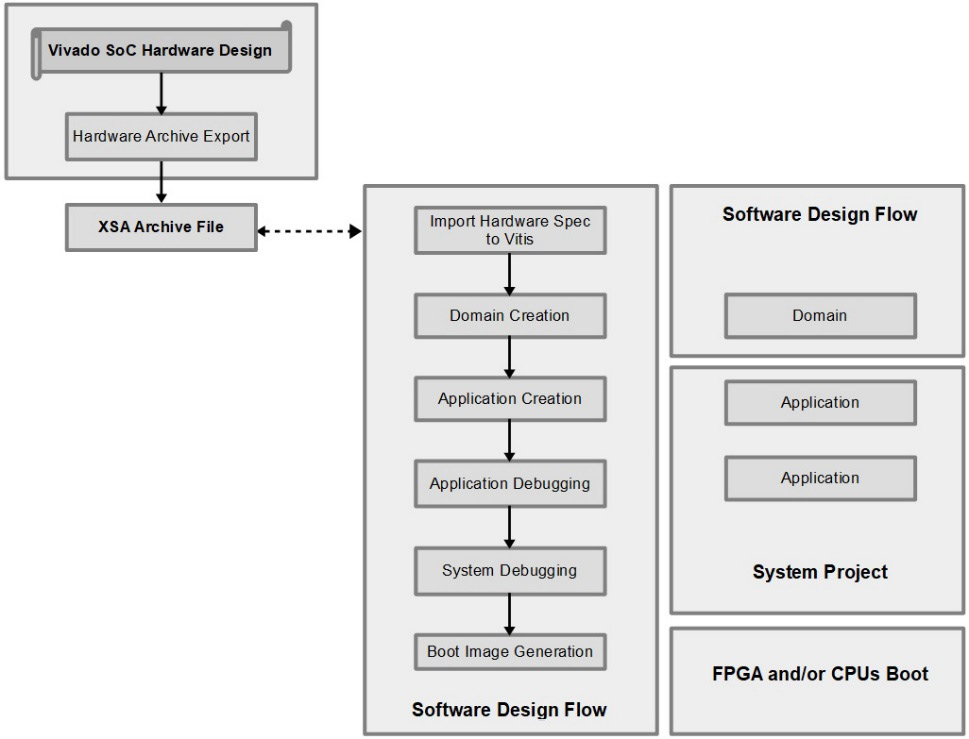
Figure 8.1 – The Vitis embedded software development steps for the ETS SoC design
ETS SoC XSA archive file generation in the Vivado IDE
First, we need to generate the XSA file within the Vivado IDE by following these steps:
- Open the ETS SoC design in Vivado and then go to File | Export | Export Hardware Platform as shown by the following figure:

Figure 8.2 – Accessing the Vivado XSA file generation wizard
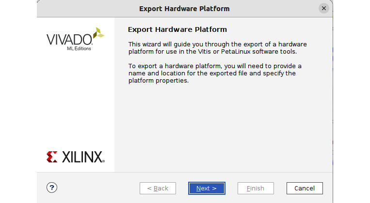
Figure 8.3 – The Vivado XSA file generation welcome screen
- In the next window, for the Output option, select the Include bitstream option so the FPGA can be programmed from Vitis IDE, as illustrated by the following figure. Click Next:
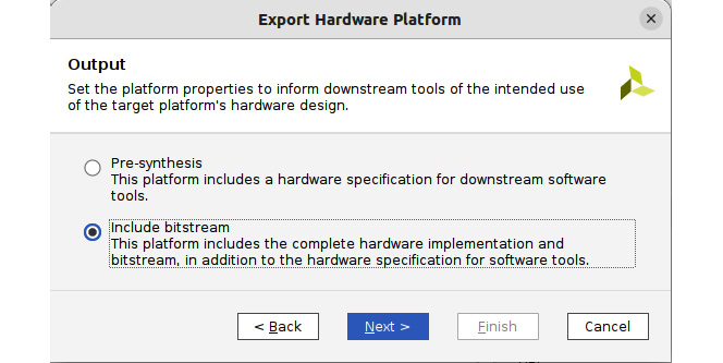
Figure 8.4 – Vivado XSA file generation options
- This Files window is used to set the name and the location of the XSA file for the ETS SoC design. Set the desired values as shown and then click Next:
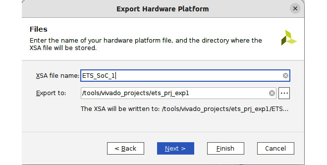
Figure 8.5 – The Vivado XSA file specification
- The following window provides a summary of the chosen settings for the XSA file generation – review these values and then click Finish to generate the XSA file:
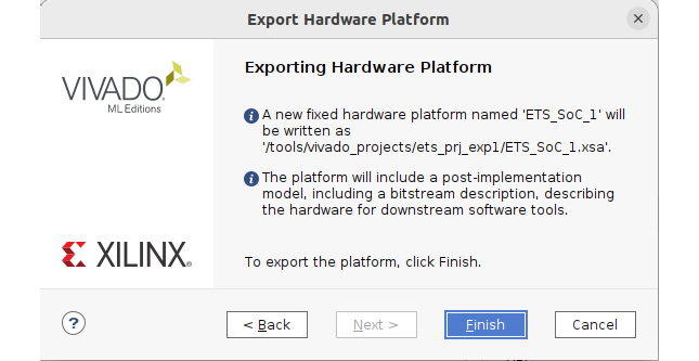
Figure 8.6 – A summary of the Vivado XSA file generation
ETS SoC software project setup in Vitis IDE
Once the XSA archive file has been created for the ETS SoC hardware design, we can use the Vitis IDE to import the ETS SoC hardware specification into the Vitis environment, which will allow us to work on the software development part of the ETS SoC. Let’s begin:
- Launch the Vitis IDE using the following command line:
$ cd <Tools_Install_Directory>/Xilinx/Vivado/2022.1/bin/
$ ./vivado
Replace <Tools_Install_Directory> with the path where you have installed Vitis on your machine or the UbuntuVM Linux VM if you are using it as a host.
- Once Vitis is up and running, we can then create the ETS SoC Vitis project using the XSA archive file of the hardware design we have produced in the Vivado IDE. When Vitis is launched, first specify a workspace for the Vitis environment, as shown in the following diagram, and then click Launch:

Figure 8.7 – Launching Vitis IDE and specifying its workspace directory
- From the Vitis IDE Welcome screen and under Project, click on Create Application Project as shown:
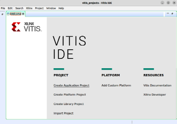
Figure 8.8 – Launching the Create Application Project menu in the Vitis IDE
- An introduction screen for the Vitis IDE Create Application Project wizard opens as shown. Review the content to refresh the information about the Vitis IDE project structure already introduced in Chapter 2, FPGA Devices and SoC Design Tools. Once done, click Next:

Figure 8.9 – The Vitis IDE project structure information
- Select the Create new platform from hardware (XSA) tab, specify the ETS SoC XSA archive file location, and fill in the Platform name field as shown. Click Next:

Figure 8.10 – Specifying the ETS SoC XSA location
ETS SoC MicroBlaze software project setup in the Vitis IDE
Once the new platform has been created in the Vitis IDE using the XSA hardware archive file we imported from Vivado, we can start the process of creating the software projects and their corresponding domains. We can start with any processor detected in the hardware platform by the Vitis IDE. Let’s start with the MicroBlaze PP of our ETS SoC project:
- Select the MicroBlaze processor hardware name instance as highlighted in the following figure. Provide the details by specifying the Application project name, System project name, and Target processor information to associate with the project as shown. Then, click Next.

Figure 8.11 – Specifying the ETS SoC MicroBlaze application project details
- Now, we can create the domain to which the ETS SoC MicroBlaze application project will link as shown. Click Next:

Figure 8.12 – Creating the ETS SoC MicroBlaze domain
- We can now select a Templates option for the ETS SoC MicroBlaze project. There are many examples to choose from. The Peripheral Tests template is a useful starting point – it will give us all the necessary information and code snippets that we can use to set, configure, and communicate with the peripherals visible to the MicroBlaze PP. We can also examine that they are operating as expected. Click Finish:
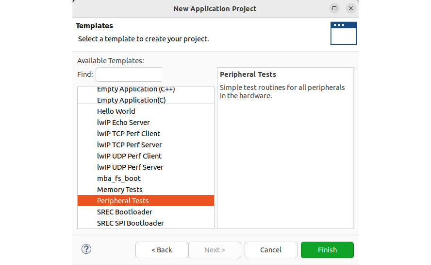
Figure 8.13 – Selecting a template for the ETS SoC MicroBlaze project
- The domain and its associated project are now created and visible in the Vitis IDE as shown. You can examine their structure and content to gain some initial familiarity with them:
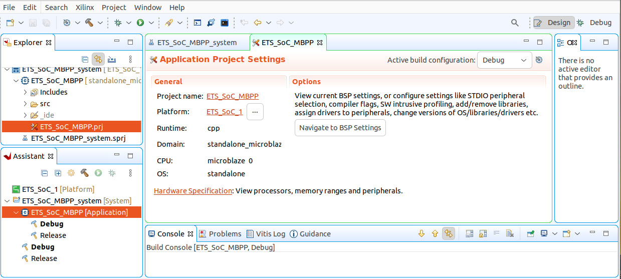
Figure 8.14 – An overview of the MicroBlaze ETS SoC project in Vitis
ETS SoC PS Cortex-A9 software project setup in the Vitis IDE
To create a second project for the ETS SoC Cortex-A9 processor in Vitis IDE, we need to create a second domain to which this second project will be linked first – then, we create the application project for the Cortex-A9 following almost the same steps as we did for the MicroBlaze PP. The only difference is that we don’t have to specify a new platform in Vitis, as it is already created:
- First, double-click on platform.spr as shown:
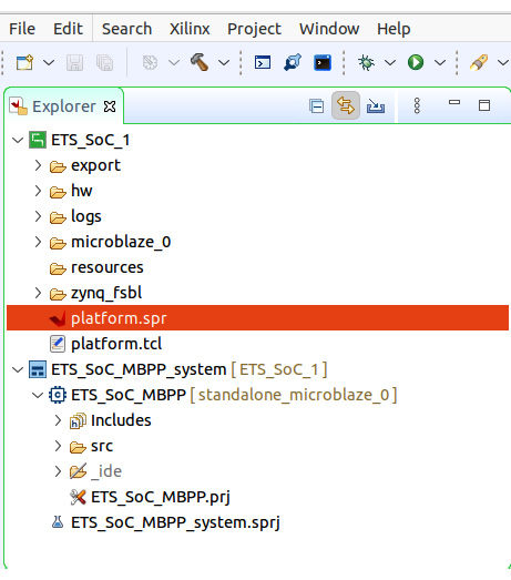
Figure 8.15 – Opening the ETS_SoC_1 platform in the Vitis IDE
- This will open the platform summary page in the Vitis IDE. Click the + sign to start a new domain creation linked to this platform. The New Domain creation wizard will be launched. Specify the information as entered in the following screenshot and click OK:

Figure 8.16 – Creating a new domain for the ETS SoC in the Vitis IDE
- The New Application Project wizard will open. Choose the first tab, Select a platform from the repository, as we already have created the ETS SoC platform using the XSA hardware archive file in previous steps. Select ETS_SoC_1 [custom] as shown and click Next:
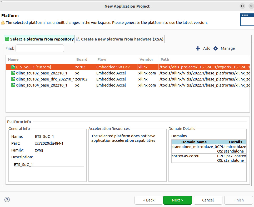
Figure 8.17 – Selecting the ETS_SoC_1 platform in the Vitis IDE
- As with when we created the new MicroBlaze PP application project, specify the details, now for the Cortex-A9 core0 project instead, as shown, and click Next:
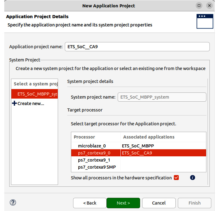
Figure 8.18 – Specifying the ETS SoC Cortex-A9 application project details
- Now, we can select the domain to which the ETS SoC Cortex-A9 New Application Project will be linked. We have just created this domain, cortex-a9-core0, in step 2. Click Next:
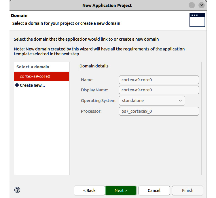
Figure 8.19 – Selecting the ETS SoC Cortex-A9 domain
- We can now select a template for the ETS SoC Cortex-A9 core0 software project. The Peripheral Tests template is a useful project to get familiarity with the Xilinx device drivers. Select the Peripheral Tests template for now and click Finish:
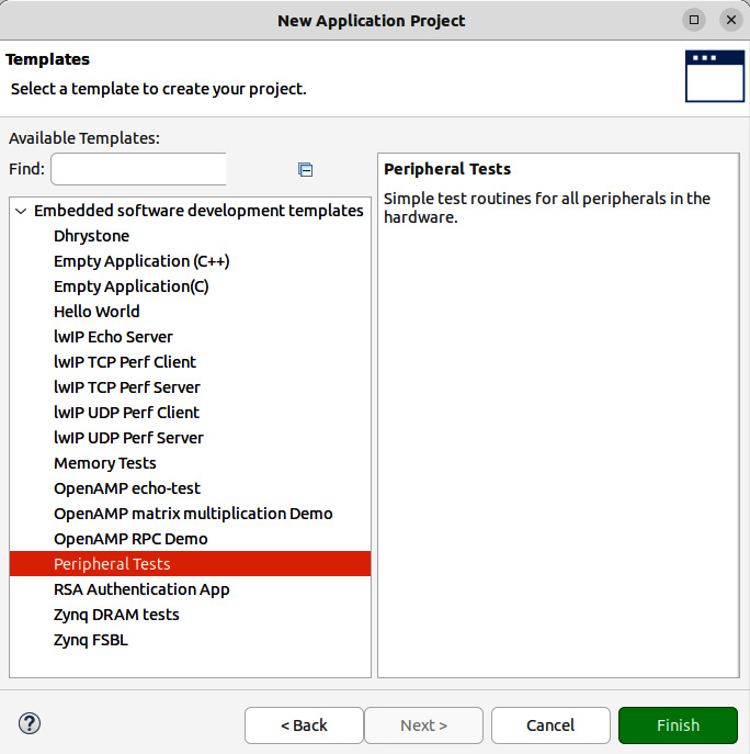
Figure 8.20 – Selecting a template for the ETS SoC Cortex-A9 project
- The second domain and its associated software project are now created for the Cortex-A9 core0 processor and visible in the Vitis IDE. You can also examine their structure and content to gain some initial familiarity with them:
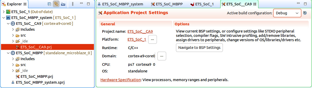
Figure 8.21 – An overview of the ETS SoC projects in Vitis
Setting up the BSP, boot software, drivers, and libraries for the software project
As can be seen in Figure 8.21, in the Application Project Settings window, BSP Settings is accessible from the Vitis IDE per application project. Also, when we first specified our ETS SoC hardware platform, by using the XSA hardware archive generated by Vivado, we selected Generate boot components (as in Figure 8.10). We should easily accomplish the remaining configuration and settings tasks for the boot, the Board Support Package (BSP), and the peripheral software drivers.
Setting up the BSP for the ETS SoC MicroBlaze PP application project
Within the Vitis IDE, we can customize the BSP, set the device drivers to use, and select the application libraries we need. We can also specify the BSP compilation options for the MicroBlaze PP ETS SoC application project. Let’s go through it by following these steps:
- To access the MicroBlaze PP application project in the Vitis IDE, simply expand the ETS_SoC_1 platform and select Board Support Package under the microblaze_0 entry, as shown in the following figure:

Figure 8.22 – Selecting the ETS SoC MicroBlaze PP BSP
- To customize the BSP for the MicroBlaze PP application project, click on Modify BSP Settings… – this will open the following window:

Figure 8.23 – Selecting the libraries for the MicroBlaze PP application project
- Select the standalone row to open the Board Support Package Settings window where we can specify the stdin and stdout devices, and all the configurations related to the Operating System (OS), which is baremetal in our case:
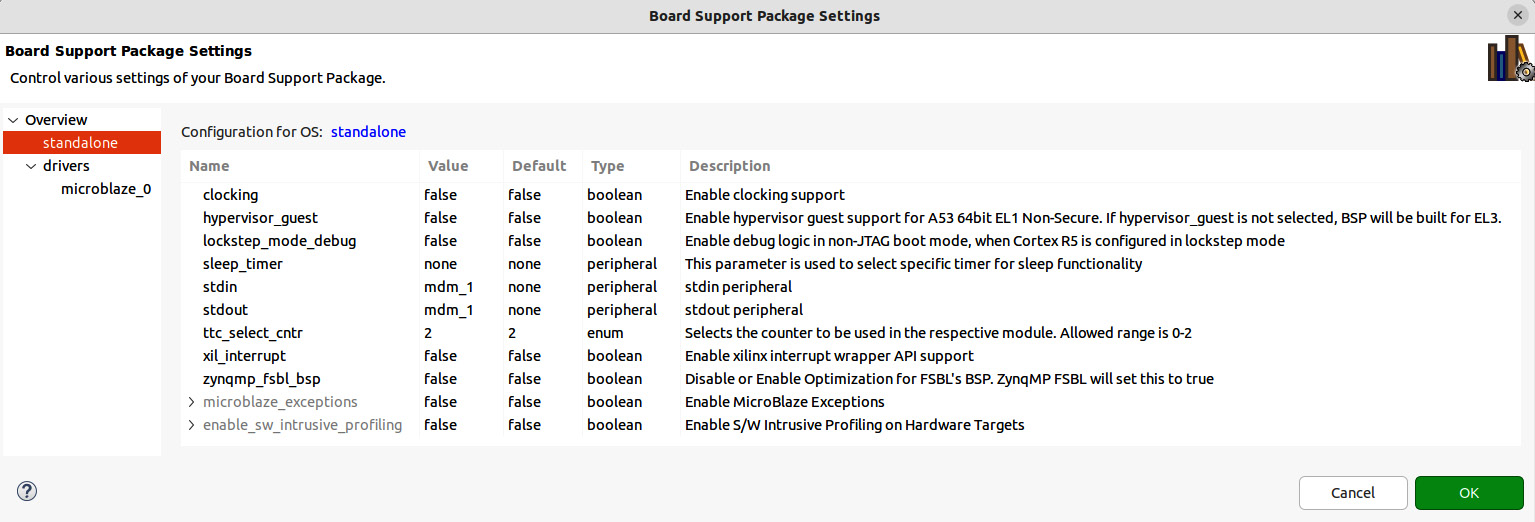
Figure 8.24 – Specifying the BSP settings for the MicroBlaze PP OS
- Select the drivers row to open the Drivers settings window as shown. Make sure that every device has an associated driver selected, as set by default:
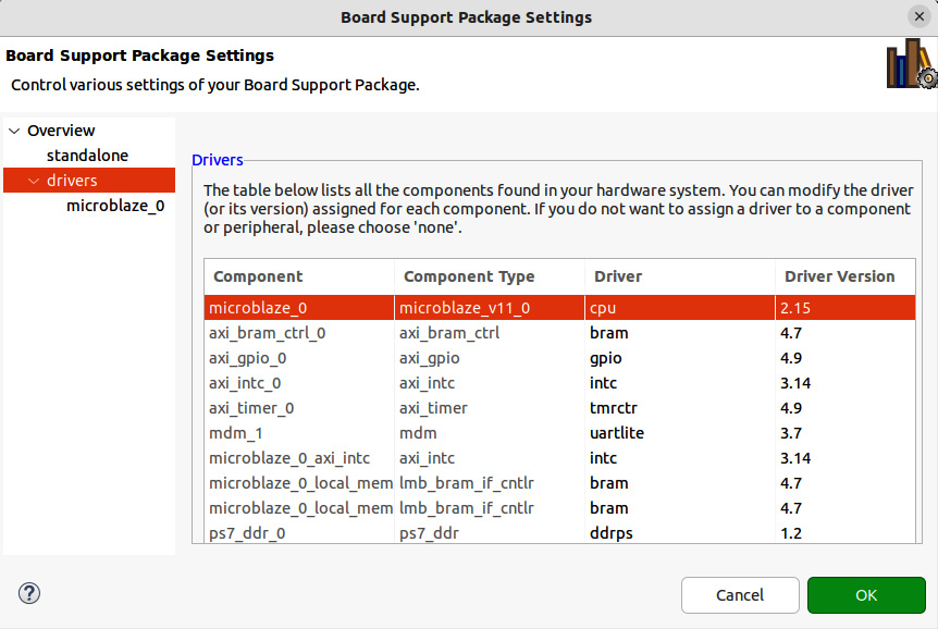
Figure 8.25 – Specifying the device drivers for the MicroBlaze PP application project
- Select the microblaze_0 row to open the BSP settings for the tools used to build the software and their options. Leave the default values as set by the Vitis IDE and click OK. This will create the necessary BSP package, as selected in the preceding steps:

Figure 8.26 – Specifying the build tools options for the MicroBlaze PP application project
Setting up the BSP for the ETS SoC Cortex-A9 core0 application project
The steps are the same as for the MicroBlaze PP, although the settings and options are different. Let’s go through them by following these steps:
- To access the Cortex-A9 core0 application project in the Vitis IDE, simply expand the ETS_SoC_1 platform and select Board Support Package under the cortex-a9-core0 entry as shown in the following figure:
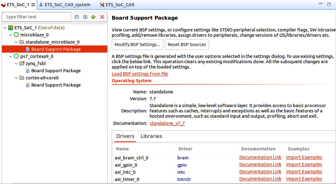
Figure 8.27 – Selecting the ETS SoC Cortex-A9 core0 BSP
- To customize the BSP for the Cortex-A9 core0 application project, click Modify BSP Settings… – this will open the following window. Select the lwIP211 library – we may choose to use its services to implement the UDP client for the Cortex-A9 processor for communication functions with the Electronic Trading Market (ETM) over the Ethernet:

Figure 8.28 – Software libraries for the Cortex-A9 core0 application project
- Select the standalone row to open the Board Support Package Settings window where we can specify the stdin and stdout devices, and all the configurations related to the OS, which is baremetal (or a standalone one) in our case:

Figure 8.29 – Specifying the BSP settings for the Cortex-A9 core0 OS
- Through this window, we can select any software library we need for the application software. Leave all the settings as their default values:
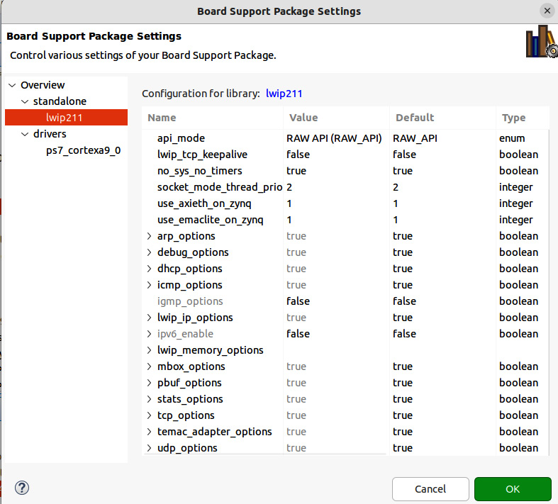
Figure 8.30 – Specifying the lwIP TCP/IP stack for the Cortex-A9 core0 OS
- Select the drivers row to open the Drivers setting window. Make sure that every device has an associated driver with it selected, as set by default:

Figure 8.31 – Specifying the device drivers for the Cortex-A9 core0 application project
- Select the ps7_cortex_a9_0 row to open Board Package Support Settings for the tools used to build the software and their options. Leave the default values as set by the Vitis IDE and click OK. This will create the necessary selected BSP package:

Figure 8.32 – Specifying the build tool options for the Cortex-A9 core0 application project
Setting up the BSP for the ETS SoC boot application project
When we first specified our ETS SoC hardware platform, by using the XSA hardware archive generated in the Vivado IDE, we selected Generate boot components as shown in Figure 8.10. As you may have noticed, this has automatically created an application project associated with the Cortex-A9 core0 and for which a BSP is also provided. We will just examine its content, so we know what is used to build such an application project to boot the system on powering up:
- To access the boot project associated with the Cortex-A9 core0 in the Vitis IDE, simply expand the ETS_SoC_1 platform and select Board Support Package under the zynq_fsbl entry, as shown by the following figure:
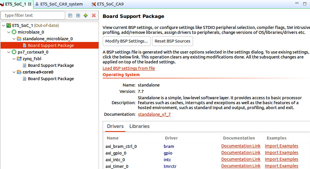
Figure 8.33 – Selecting the ETS SoC boot application BSP
- This will open the BSP entry of the boot application project associated with the Cortex-A9 core0. We can see that the boot library settings use a Generic Fat Filesystem, as well as some security software libraries, provided by Xilinx and automatically set by the Vitis IDE. Leave the settings as their default values:
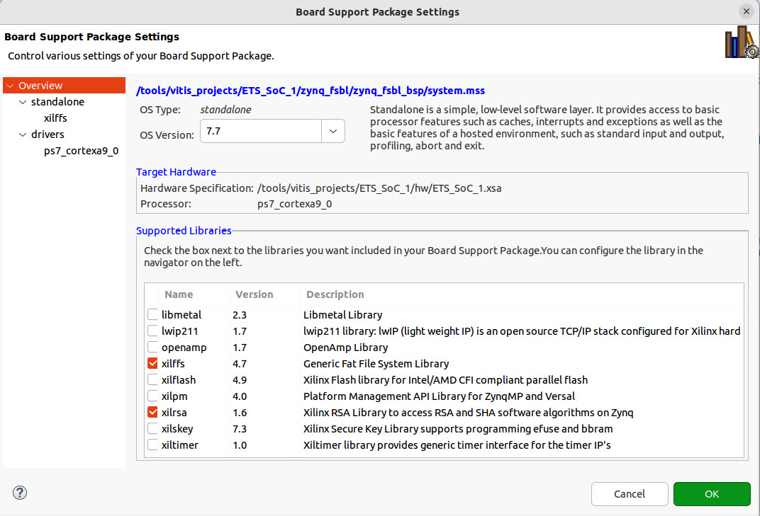
Figure 8.34 – Library settings for the Cortex-A9 core0 boot application project
- Select the ps7_cortex_a9_0 row to open the BSP settings for the tools used to build the software and their options as shown in the following figure. Leave the default values as set by the Vitis IDE and click OK. This will create the necessary BSP package, as selected in the preceding steps:
Figure 8.35 – Specifying the build tool options for the boot application project
Defining the distributed software microarchitecture for the ETS SoC processors
Thus far in this chapter, we have learned how a software project is created using the Vitis IDE, associated with a specific processor in the ETS SoC project, and how its BSP is configured. We can now delve into the software application-building process. We will develop a software microarchitecture for each processor core used in the ETS SoC design first. This will be based on the system architecture we developed in Chapter 6, What Goes Where in a High-Speed SoC Design, and the hardware implementation choices we made in Chapter 7, FPGA SoC Hardware Design and Verification Flow, such as the IPC mechanisms in both directions between the Cortex-A9 and the MicroBlaze PP processors. We can now revisit some remaining open items in the SoC system architecture. We have also defined the Electronic Trading Market Protocol (ETMP); therefore, the filtering tasks are easily identifiable by reading the UDP packet payload of the ETMP. Let’s start by redrawing the system hardware microarchitecture in a simplified view with the hardware implementation options we have made. We will also revisit the software-to-hardware communication model we created in Chapter 6, What Goes Where in a High-Speed SoC Design, and fill in any missing microarchitectural detail necessary for a correct and complete exchange of information between them.
A simplified view of the ETS SoC hardware microarchitecture
Following the ETS SoC initial system architecture definition, we have made some choices for the hardware implementation based on the microarchitecture proposal. We can redraw the full ETS SoC microarchitecture as shown in the following diagram:

Figure 8.36 – A simplified diagram of the ETS SoC microarchitecture
The IPC interrupts from the Cortex-A9 to the MicroBlaze PP are generated using the AXI INTC0, where the doorbell registers are implemented within the AXI interrupt controller. When the Cortex-A9 needs to interrupt the MicroBlaze PP, it writes to the corresponding bit in the AXI INTC0 Interrupt Status Register (ISR), which then triggers an interrupt towards the MicroBlaze PP. Dealing with this interrupt from the MicroBlaze PP is the same as dealing with any hardware IP-generated interrupt. In the opposite direction, the process is the same – the MicroBlaze PP writes to the AXI INTC1 ISR, which then communicates through the signal output from the AXI INTC1, which is connected to the Cortex-A9 GIC input. The Cortex-A9 will deal with it as it would deal with any other hardware IP-generated interrupt.
A summary of the data exchange mechanisms for the ETS SoC Cortex-A9 and the MicroBlaze IPC
The AXI BRAM will host the circular buffer via which Acceleration Request Entries (AREs) are logged by the Cortex-A9 upon identifying an Ethernet frame for a UDP packet. The Ethernet interface uses its DMA engine to copy the received Ethernet frame from the Ethernet interface’s internal buffer to the OCM memory. The Ethernet interface DMA buffer descriptors are created by the Cortex-A9 processor (at startup and before arming the Ethernet interface’s DMA engine for receive operations). The DMA buffer descriptors are also created in a large circular buffer in the AXI BRAM memory – they are going to be used by the MicroBlaze PP, as it performs the filtering tasks for the Cortex-A9, so storing them in the AXI BRAM will lower the latency of their access at acceleration time. The Cortex-A9 software performs an initial frame inspection by checking the Ethernet Type field of the received Ethernet frame – if it finds it to be a UDP packet, it constructs an ARE data structure, which it puts in the aforementioned ARE circular buffer hosted in the AXI BRAM. When the Cortex-A9 populates the ARE circular buffer with a fresh entry, it rings the doorbell for the MicroBlaze PP by writing to the AXI INTC0 ISR, which will then trigger the corresponding interrupt toward the MicroBlaze PP. The MicroBlaze PP is the consumer of the ARE circular buffer entries, whereas the Cortex-A9 is the producer. The MicroBlaze PP maintains its read pointer (MBARERdPtr) of the ARE circular buffer, whereas the Cortex-A9 writes to it and maintains the write pointer (CA9AREWrPtr). Both pointers are visible to both processors at any time – these pointers are hosted in the AXI BRAM memory space as well. Every ARE has a recycling bit so that when the MicroBlaze PP consumes the entry and processes the request, it marks it as ready for a subsequent reuse. The following diagram from Chapter 6, What Goes Where in a High-Speed SoC Design, illustrates the filtering tasks offloaded to the MicroBlaze PP:

Figure 8.37 – An ETS low-latency path for a hardware-to-software interaction
When the MicroBlaze PP inspects the UDP packet associated with an ARE (there may be many UDP packets associated with a single ARE request, as we will see later), it is simply looking for a filter match. We have highlighted three filters thus far (buy, sell, and log). A specific UDP packet may match both the sell and log filters or both the buy and log filters. When the MicroBlaze PP finds a filter match for a specific symbol on a UDP packet, it puts its descriptor address in the corresponding response queue and rings the corresponding doorbell for the Cortex-A9. We have considered five queues in the architecture definition:
- The buy queue (BuyQ) that the MicroBlaze PP fills with the descriptors of the Ethernet frames carrying the UDP packet with a buy filter match on their symbol
- The sell queue (SellQ) that the MicroBlaze PP fills with the descriptors of the Ethernet frames carrying the UDP packet with a sell filter match on their symbol
- The market data queue (MdataQ) that the MicroBlaze PP fills with the descriptors of the Ethernet frames carrying the UDP packet with a market data filter match on their symbol
- The management data queue (MgmQ) that the MicroBlaze PP fills with the descriptors of the Ethernet frames carrying the UDP packet with a management message
- The DMA descriptor recycle queue (DDRQ) where the MicroBlaze PP puts the address of the descriptors of the Ethernet frames it has dealt with – this queue may seem redundant but can be used as a checking mechanism by the Cortex-A9 garbage collection tasks
Every time the MicroBlaze PP writes a descriptor in a specific queue, it rings the doorbell associated with it by sending a software-triggered interrupt to the Cortex-A9 using the AXI INTC1 mechanism.
All the queues described here are also circular buffers, for which the MicroBlaze PP is now the entry producer and the Cortex-A9 is the entry consumer. Every queue has two pointers, a write pointer owned by the MicroBlaze PP and a read pointer owned by the Cortex-A9. Both pointers are visible to both CPUs. All the filtering results queues are hosted in the AXI BRAM memory as well as the write and read pointers. The following figure provides a summary of the filtering match queues and their associated pointers:

Figure 8.38 – ETS SoC filtering match data queues and associated pointers
The ETMP protocol overview
The Electronic Trading Market Protocol (ETMP) defines a single-length UDP packet payload (320 bits or 40 bytes) and has many fields, as defined in the following figure:
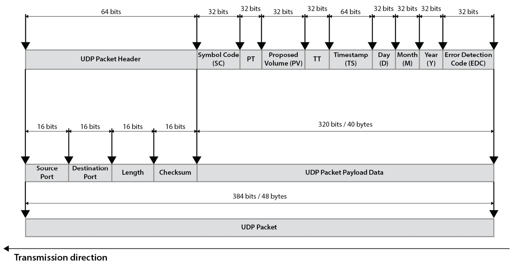
Figure 8.39 – The ETMP packet layout
The UDP header adds another 64 bits of data to the packet, resulting in an ETMP UDP frame of 384 bits or 48 bytes, as illustrated by the preceding figure. The following table reminds us of the ETMP fields that the MicroBlaze and Cortex-A9 software needs to use:
|
Field |
Length in bits |
Description |
|
Symbol Code (SC) |
32 |
The financial traded product symbol code. Every financial product has a unique code assigned by the ETM when the product is first introduced to the ETM. |
|
Packet Type (PT) |
32 |
States whether this is a Market Management packet or a Market Data packet. 0b0: Market Data packet. 0b1: Management packet. |
|
Proposed Volume (PV) |
32 |
The proposed maximum volume for a sell or buy action. Partial proposals of trade can be made by the ETS if interested in the symbol. |
|
Transaction Type (TT) |
32 |
The transaction type associated with this financial product, buying, or selling: 0b0: Buying. 0b1: Selling. |
|
Timestamp (TS) |
64 |
This is the timestamp logging when the UDP packet left the ETM servers. |
|
Day (D) |
32 |
Encodes the day when the UDP packet was sent. |
|
Month (M) |
32 |
Encodes the month when the UDP packet was sent. |
|
Year (Y) |
32 |
Encodes the year when the UDP packet was sent. |
|
Error Detection Code (EDC) |
32 |
CRC32 computed over all the ETMP packets excluding itself (over the 288 bits). |
Table 8.1 – A description of the ETMP packet format and fields
For the EDC, there are open source implementations of the CRC32 algorithm in C that we can use for now in this design example. We will revisit this in Part 3 of this book when we look at profiling and hardware acceleration techniques in detail to modify the design to include a hardware-based CRC32 implementation.
The ETS SoC system address map
The system address map allows us to locate the physical address of all the mapped devices and memories in the SoC address space, as seen from the Cortex-A9 cluster AXI interfaces and the MicroBlaze PP. This gives us an idea of how to initialize the necessary software pointers when we want to allocate their associated storage, for example, as we develop the software applications for the SoC design.
The ETS SoC MicroBlaze PP system address map
To access the MicroBlaze PP system address map, we can simply click on the Hardware mapping details in the Vitis IDE’s main window. The MicroBlaze PP system address map looks as follows:
|
IP |
Base Address |
High Address |
Description |
|
LMB memory |
0x0000_0000 |
0x0000_3FFF |
SLMB |
|
A_AXI_GPO.PS7_DDR_0 |
0x2000_0000 |
0x3FFF_FFFF |
PL AXI Interconnect |
|
AXI Timer |
0x4000_0000 |
0x4000_FFFF |
PL AXI Interconnect |
|
MicroBlaze Debug MDM |
0x4040_0000 |
0x4040_0FFF |
PL AXI Interconnect |
|
AXI INTC0 |
0x4080_0000 |
0x4080_FFFF |
PL AXI Interconnect |
|
AXI GPIO |
0x4120_0000 |
0x4120_FFFF |
PL AXI Interconnect |
|
AXI BRAM memory |
0x4200_0000 |
0x4200_3FFF |
PL AXI Interconnect |
|
AXI INTC1 |
0x4240_0000 |
0x4240_FFFF |
PL AXI Interconnect |
Table 8.2 – The MicroBlaze PP system address map
The ETS SoC Cortex-A9 system address map
To access the Cortex-A9 system address map, we can simply click on the hardware mapping details in the Vitis IDE’s main window. The Cortex-A9 system address map looks as follows:
|
IP |
Base Address |
High Address |
Description |
|
PS7_RAM_0 |
0x0000_0000 |
0x0002_FFFF | |
|
PS7_DDR_0 |
0x0010_0000 |
0x3FFF_FFFF |
Direct port mapping |
|
AXI GPIO |
0x4120_0000 |
0x4120_FFFF |
PL AXI Interconnect |
|
AXI BRAM memory |
0x4200_0000 |
0x4200_3FFF |
PL AXI Interconnect |
|
AXI INTC1 |
0x4240_0000 |
0x4240_FFFF |
PL AXI Interconnect |
|
PS7_UART_1 |
0xE000_1000 |
0xE000_1FFF |
PS AXI Central Interconnect |
|
PS7_I2C_0 |
0xE000_4000 |
0xE000_4FFF |
PS AXI Central Interconnect |
|
PS7_GPIO_0 |
0xE000_A000 |
0xE000_AFFF |
PS AXI Central Interconnect |
|
PS7_Ethernet_0 |
0xE000_B000 |
0xE000_BFFF |
PS AXI Central Interconnect |
|
PS7_QSPI_0 |
0xE000_D000 |
0xE000_DFFF |
PS AXI Central Interconnect |
|
PS7_IOP_BUS_CFG_0 |
0xE020_0000 |
0xE020_0FFF |
PS AXI Central Interconnect |
|
PS7_SLCR_0 |
0xF800_0000 |
0xF800_0FFF |
Internal to the CPU Cluster |
|
PS7_DMA_NS |
0xF800_4000 |
0xF800_4FFF |
PS AXI Central Interconnect |
|
PS7_DMA_S |
0xF800_3000 |
0xF800_3FFF |
PS AXI Central Interconnect |
|
PS7_DDRC_0 |
0xF800_6000 |
0xF800_6FFF | |
|
PS7_DEV_CFG_0 |
0xF800_7000 |
0xF800_70FF |
PS AXI Central Interconnect |
|
PS7_XADC_0 |
0xF800_7100 |
0xF800_7120 |
PS AXI Central Interconnect |
|
PS7_AFI_0 |
0xF800_8000 |
0xF800_8FFF | |
|
PS7_AFI_1 |
0xF800_9000 |
0xF800_9FFF | |
|
PS7_AFI_2 |
0xF800_A000 |
0xF800_AFFF | |
|
PS7_AFI_3 |
0xF800_B000 |
0xF800_BFFF | |
|
P7_OCMC_0 |
0xF800_C000 |
0xF800_CFFF | |
|
PS7_CORESIGHT_0 (1) |
0xF880_0000 |
0xF88F_FFFF |
PS AXI Central Interconnect |
|
PS7_PMU_0 |
0xF889_3000 |
0xF889_3FFF | |
|
PS7_GPV_0 |
0xF890_7000 |
0xF89F_FFFF |
PS AXI Central Interconnect |
|
PS7_SCUC_0 |
0xF8F0_0000 |
0xF8F0_00FC |
Internal to the CPU Cluster |
|
PS7_SCUGICC_0 |
0xF8F0_0100 |
0xF8F0_01FF |
Direct mapping |
|
PS7_SCUTIMER_0 |
0xF8F0_0600 |
0xF8F0_061F |
Internal to the CPU Cluster |
|
PS7_GLOBALTIMER_0 |
0xF8F0_0200 |
0xF8F0_02FF | |
|
PS7_SCUWDT_0 |
0xF8F0_0620 |
0xF8F0_06FF |
Internal to the CPU Cluster |
|
PS7_INTC_DIST |
0xF8F0_1000 |
0xF8F0_1FFF |
Internal to the CPU Cluster |
|
PS7_L2CACHEC_0 |
0xF8F0_2000 |
0xF8F0_2FFF |
Internal to the CPU Cluster |
|
PS7_QSPI_LINEAR_0 |
0xFC00_0000 |
0xFCFF_FFFF |
PS AXI Central Interconnect |
|
PS7_RAM_1 |
0xFFFF_0000 |
0xFFFF_FDFF |
Table 8.3 – The Cortex-A9 system address map
(1) CoreSight is the ARM debug infrastructure used with ARM processors.
The Ethernet MAC and its DMA engine software control mechanisms
One of the most important IPs and one of the most complex peripherals used in the ETS SoC is the Ethernet interface. It connects the ETS SoC to the ETM switch, via which the UDP packets for processing are received using its DMA engine. We need to create the DMA buffer descriptors circular buffer so the received Ethernet frames will automatically be copied to the target memory using the information provided by the DMA buffer descriptors. We have already decided that the circular buffer containing the Ethernet interface DMA buffer descriptors will be hosted in the AXI BRAM memory. This memory should be marked as non-cacheable by both processors since the SoC interconnect is non-coherent. The DMA engine may change data in the DMA buffer descriptors, whereas the processors have no way of knowing about this if they keep working on the local copy that they hold in their respective data cache. For the Ethernet frames data itself, we can target any memory within the ETS SoC as far as it is visible to both the Cortex-A9 and the MicroBlaze PP processors. From the system address maps in Tables 8.2 and 8.3, we can see that both the AXI BRAM and the ETS SoC DDR memory can host the Ethernet frames and we can therefore use the DDR memory for this buffering given its larger capacity. We are interfacing to the DDR memory through the General-Purpose AXI interfaces (GP0) since we are not expecting any challenging traffic over this path, but the optimal option would have been using the High-Performance AXI interfaces, which connect directly to the memory. We can easily change this post-deployment if we discover that there is an issue with meeting the target performance using the AXI GP interface. To use the Ethernet interface in the ETS SoC software, it needs to be initialized by the Cortex-A9 software – here are the steps required to get the Ethernet interface ready for use by the software application:
- Unlock the System Level Control Register so control registers can be written by software.
- We need to configure the clocking for the 1 Gbps operations.
- Now, we can lock the System Level Control Register from the software.
- We can now initialize the Ethernet interface using the following functions provided by the Ethernet drivers:
Config = XEmacPs_LookupConfig(EmacPsDeviceId);
Status = XEmacPs_CfgInitialize(EmacPsInstancePtr, Config,Config->BaseAddress);
- We can now set the MAC Address of the Ethernet interface using the following Ethernet driver function:
Status = XEmacPs_SetMacAddress(EmacPsInstancePtr, EmacPsMAC, 1);
- Now, we can set the callback functions to handle the send event that follows the execution of a transmission operation, a receive event that follows a receive operation, and an error event in case the Ethernet interface detects an error:
Status = XEmacPs_SetHandler(EmacPsInstancePtr,
XEMACPS_HANDLER_DMASEND,
(void *) XEmacPsSendHandler,
EmacPsInstancePtr);
Status |= XEmacPs_SetHandler(EmacPsInstancePtr,
XEMACPS_HANDLER_DMARECV,
(void *) XEmacPsRecvHandler,
EmacPsInstancePtr);
Status |= XEmacPs_SetHandler(EmacPsInstancePtr,
XEMACPS_HANDLER_ERROR,
(void *) XEmacPsErrorHandler,
EmacPsInstancePtr);
More steps and further details of the Ethernet interface configuration are still required for a full functional set up.
Information
The details of the Ethernet interface driver functions used in these code snippets are available from Xilinx at https://xilinx-wiki.atlassian.net/wiki/spaces/A/pages/18841610/AXI+Ethernet+Standalone+Driver.
Next is the Ethernet DMA operation setup for the receive side – it can also be started using the following steps:
- Using the following BSP function, we can make the 1 MB region where the AXI BRAM is mapped (as seen by the Cortex-A9 processor) uncacheable:
// The memory is made uncacheable by writing the MMU TLB using:
Xil_SetTlbAttributes(0x42000000, 0xc02);
- We can now define the DMA buffer descriptor’s circular buffer in the AXI BRAM memory using the following driver functions:
XEmacPs_BdClear(&BdTemplate);
XEmacPs_BdRingCreate(&(XEmacPs_GetRxRing(EmacPsInstancePtr)),
RX_BD_LIST_START_ADDRESS,
RX_BD_LIST_HIGH_ADDRESS, XEMACPS_BD_ALIGNMENT,
RXBD_CNT);
XEmacPs_BdRingClone(&(XEmacPs_GetRxRing(EmacPsInstancePtr)),
&BdTemplate, XEMACPS_RECV);
Once the configuration and initialization steps are performed using the Xilinx-provided Ethernet interface driver functions, the system setup can be performed. We obviously also need to set up the interrupt controller and then enable the Ethernet interface interrupts. Transmit and receive operations using the Ethernet interface can then be started by ringing the DMA doorbell.
The AXI INTC software control mechanisms
The AXI INTC is used for managing the system functional interrupts of the MicroBlaze PP, and for generating the IPC software-generated interrupts between the Cortex-A9 and the MicroBlaze processors. Xilinx Vitis generates all the necessary driver functions to configure and use the AXI INTC. The following steps in the source code list how these are used in the Peripheral Tests template software application:
// Initialize the interrupt controller driver so that it is ready to use.
XIntc_Initialize(IntcInstancePtr, DeviceId);
// Initialize the exception table.
Xil_ExceptionInit();
// Register the interrupt controller handler with the exception table.
Xil_ExceptionRegisterHandler(XIL_EXCEPTION_ID_INT,(Xil_ExceptionHandler)XIntc_DeviceInterruptHandler, (void*) 0);
// Enable exceptions.
Xil_ExceptionEnable();
// Start the interrupt controller such that interrupts are
// enabled for all devices that cause interrupts.
XIntc_Start(IntcInstancePtr, XIN_REAL_MODE);
To trigger a software interrupt using the AXI INTC, as we have introduced in Chapter 7, FPGA SoC Hardware Design and Verification Flow, we simply need to write 0b1 to the corresponding bit in the ISR register. The following AXI INTC driver function can be used to achieve this:
XIntc_Out32(IntcBaseAddress + XIN_ISR_OFFSET, INTC_DEVICE_INT_MASK);Quantitative analysis and system performance estimation
The Ethernet frames broadcasted by the ETM are 86 bytes long. At 1 Gbps (128 MB/s), we are looking at a maximum receive rate of an Ethernet frame every 640 ns, as estimated by the following formula:

The maximum rate at which the ETM can send the Ethernet frames of 86 bytes each is a frame every 640 ns. Since the PL design is running at 100 MHz, that only gives the MicroBlaze PP 64 cycles to process a UDP frame. This is impossible to meet with the current proposal. This is obviously a very high rate for the type of accelerator we have decided to use in the proposal microarchitecture. We have chosen a MicroBlaze PP as a convenient way of also learning how to use it to build an FPGA-embedded processor as a coprocessor to the Cortex-A9. To be realistic, we need the ETM Ethernet transfer rate to be much lower than sending one packet every 640 ns. Without any profiling exercise on the MicroBlaze PP software, which we haven’t written yet, we can’t tell for sure how many cycles the MicroBlaze PP needs to look up the fields in the ETMP packet, detect the filter matches, and then produce a result for the Cortex-A9 via the envisaged mechanisms, and send a notification via the IPC interrupts. We also have decided to use a CRC32 algorithm in software, which will only make matters worse in terms of performance, but this can easily be fixed by designing a hardware-based CRC32 calculator and adding it as a coprocessor to the MicroBlaze PP itself. When we cover profiling and hardware acceleration in Part 3, we will keep these considerations in mind. We estimate that performing the CRC32 computing in hardware will be at least an order of magnitude faster than using the MicroBlaze PP itself to perform it. We estimate that for a GNU-based CRC32 software calculator, we need about 16 clock cycles per byte of data – that is, for a full ETMP UDP payload of 40 bytes, it shall amount to 640 clock cycles. Using a hardware-based calculator will require about a byte per clock cycle – that is, a total of 40 clock cycles.
To estimate the lookup rate for a filter match beside the CRC32 computing, and once we propose the full software microarchitecture for the MicroBlaze PP, we should be in a better position to put some numbers to the operations to perform per received Ethernet frame, therefore allowing us to predict how many system clock cycles the MicroBlaze PP will need to perform the necessary operations.
The ETS SoC Cortex-A9 software microarchitecture
Following a power-up or a cold system boot, the Cortex-A9 will perform the following tasks in software:
- Configure all the necessary system IPs including its MMU and caches
- Create the DMA buffer descriptors and arm the Ethernet MAC DMA receive engine
We can list the tasks that need to be executed following the reception of an IPC interrupt from the MicroBlaze PP when a filter is matched for a specific UDP packet. The interrupt service routine can set a flag, which the main() function can then use as a trigger to pass execution to the corresponding function associated with it. We can obviously benefit from the services of a Real-Time Operating System (RTOS) to help with performing the scheduling and task priority management, as well as providing a TCP/IP stack. Via the stack, we can then send the TCP packets back to the ETM when a buy or sell action is the result. We can also use its filesystem and flash management services to log the data of interest. As for the management packets received from the ETM, we can pass them over the PCIe link toward the host server, which deals with the policy and adjusts the algorithms that execute the trading decisions running on the Cortex-A9 software. In this chapter, we will only focus on the acceleration path back to the Cortex-A9, whereas in Part 3, when we introduce the use of an RTOS with the ETS SoC, we can complete the user application using these services. The following diagram provides a software microarchitecture based on the analysis performed thus far:
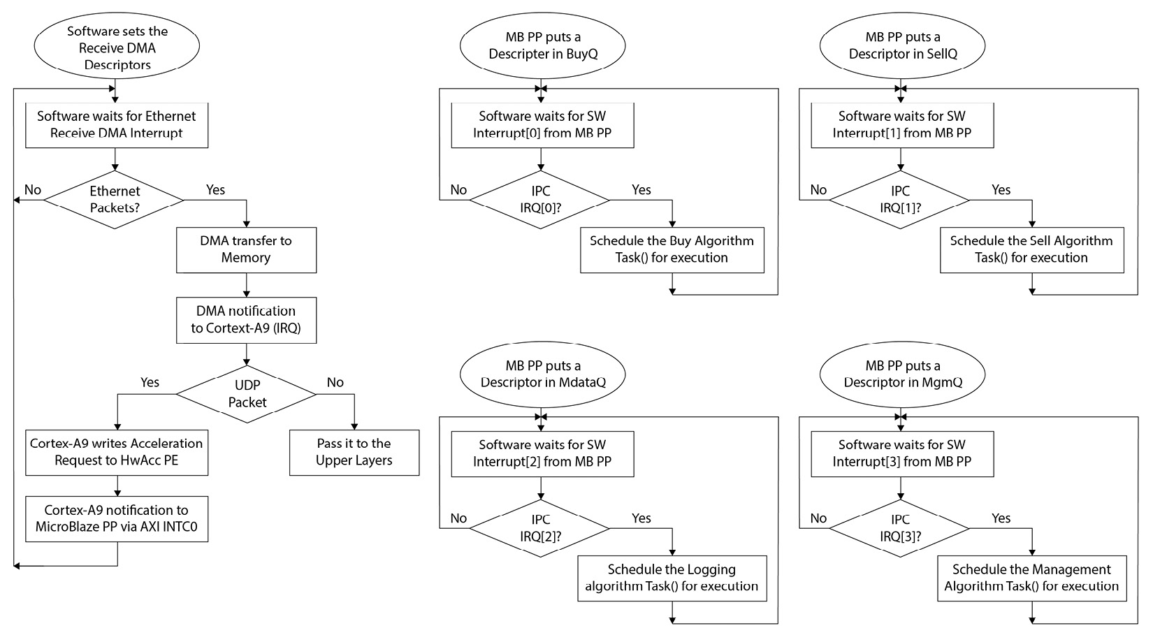
Figure 8.40 – The Cortex-A9 receive path software microarchitecture
The ETS SoC MicroBlaze PP software microarchitecture
Following a power-up or a cold system boot, the MicroBlaze PP will perform the following tasks in software:
- Configure all the necessary system IPs
- Go through the process of setting up the ISRs (ISR()) associated with the expected tasks to perform
We can list the tasks that need to be executed following the reception of an IPC interrupt from the Cortex-A9 when an ARE is received via the ARE circular buffer. The ISR function, ISR(), can set a flag, which the main() function can then use as a trigger to pass execution to the corresponding function associated with it. There will be no nested interrupt support nor filtering job preemption, so when the MicroBlaze PP detects an IPC interrupt and start executing it, it disables the interrupts and will only re-enable them upon finishing the filtering of the descriptor(s) associated with the received ARE. This task includes the generation of a response by putting the filter matching the descriptor into its destination response queue and then writing to the AXI INTC1 corresponding bit to generate the IPC interrupt toward the Cortex-A9 processor. In fact, the MicroBlaze PP, when it falls behind on the filtering and while it still has entries in the ARE circular buffer, can continue to process them until it reaches the end of the queue. When it reaches the end of the queue, it can go to sleep, pending an IPC interrupt from the Cortex-A9 for further acceleration requests. The MicroBlaze PP will need to manage the circular buffer read, MBARERdPtr. The following diagram provides a software microarchitecture based on the analysis performed thus far:
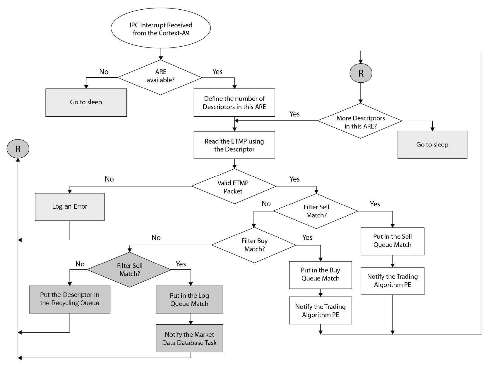
Figure 8.41 – The MicroBlaze PP software microarchitecture
Building the user software applications to initialize and test the SoC hardware
The Vitis IDE is based on Eclipse – it inherits all the source code editing features and project management Eclipse is known for. Let’s explore the software project structure and how source code files can be added or removed from the project, for example:
- In the Vitis IDE Explorer window, expand the src folder under one of the projects, such as ETS_SOC_CA9 – all the included sources will be listed. Double-click on the testperiph.c file to open it in the source code editor:

Figure 8.42 – Browsing the ETS SoC projects source code
- The source file is now opened in the Vitis IDE as shown:

Figure 8.43 – Editing the ETS SoC project source code
Specifying the linker script for the ETS SoC projects
Once we have all the source code in place, such as for the ETS SoC design test applications of the Cortex-A9 and the MicroBlaze processors, we need to specify a linker script for each of the projects which will assign a physical location to the different sections of the executable files. The Vitis IDE has a graphical tool to edit and generate the linker script file. For both projects, follow the next steps, which will explain the linker script concept and how it can be used to assign a specific section of the executable file to a specific region of memory visible to the Cortex-A9 processor:
- To launch the Linker Script editor, double-click on the lscript.ld entry from the Explorer menu as shown:

Figure 8.44 – Launching the linker script in the Vitis IDE
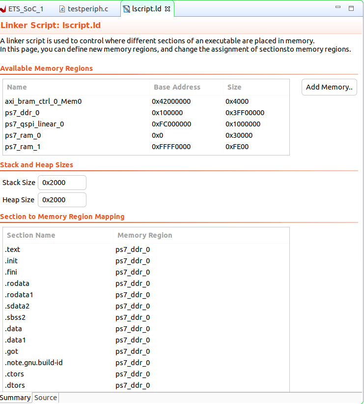
Figure 8.45 – Editing the linker script in the Vitis IDE
Setting the compilation options and building the executable file for the Cortex-A9
From the Vitis IDE, we can specify the Cortex-A9 compiler options by following these steps:
- Right-click on the Cortex-A9-associated project in the Vitis IDE Explorer and click Properties:

Figure 8.46 – Accessing the build settings for the Cortex-A9 project
- Build Settings will open for the project as indicated in the following figure. Under the C/C++ Build row, click Settings. Under Arm v7 gcc assembler, click General. Then, in front of Include Paths -I, click the + sign as shown:

Figure 8.47 – Accessing the build settings for the Cortex-A9 project
The Add directory path window will open as shown. Browse to where the BSP <include> directory is located on your machine. It should be under <project location path>/ETS_SoC_1/ps_7_cortexa9_0/cortex-a9-core0/bsp/ps7_cortexa9_0/. Once located, select it and click OK:

Figure 8.48 – Adding the BSP <include> directory to the software project in the Vitis IDE
- This will pass the BSP <include> directory to the -I compiler options. If this is not specified, the project won’t build:
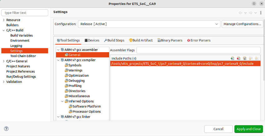
Figure 8.49 – The BSP <include> directory added to the -I compiler option in the Vitis IDE
- Now, the projects can be built in the Vitis IDE. There are many ways to do this – for example, by going to the main menu and selecting Project | Build all…. The BSPs and all the binaries will be built, as shown by the following figure:
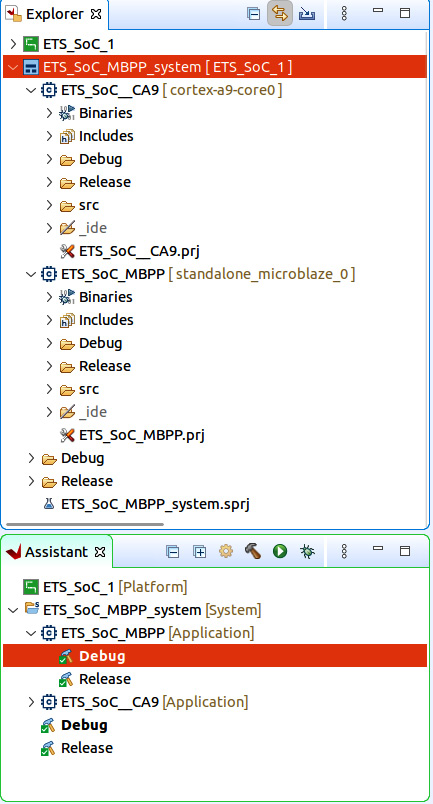
Figure 8.50 – Building all the ETS SoC software projects in the Vitis IDE
We have now built all the application software associated with the ETS SoC project using the Vitis IDE. This will then allow us to proceed to the next step of the design process, in which we will be looking at the hardware and software integration step, and we will cover this in the next chapter.
Summary
In this chapter, we started by exporting the ETS SoC hardware design into the Vitis IDE by generating the XSA file. We then used it in the Vitis IDE to create a custom hardware system definition for which we want to develop the application software. We have seen how a domain can be created in Vitis IDE for a given processor, and how a template application project can be generated and linked to a given domain. We then explored the BSP components and how they can be set up in the Vitis IDE for both the MicroBlaze and the Cortex-A9 processors to specify the Xilinx device drivers and the available software libraries. We then went back to the ETS SoC system architecture and we developed the software microarchitecture for both the Cortex-A9 receive path and the MicroBlaze PP acceleration software. We started doing some analytical work on the system performance and how we can compute some metrics for our ETS SoC design knowing only a few system parameters and without building the full design to measure them. We have also gained the necessary familiarity with how the software build options are performed in the Vitis IDE, including the use of the graphical interface to generate the linker script, as well as how the compiler options are specified within the Vitis IDE. We finally built the test applications linked to the ETS SoC project that we generated as templates when we first created the domains in Vitis. In this chapter, we performed all the necessary steps and gained most of the important knowledge required to be able to complete the full ETS SoC software applications building.
In the next chapter, we will complete the picture of what is specific to the FPGA SoC designs. We will be able to take the software binaries and combine them with the hardware bitstream to boot the complete SoC. We will also address all the aspects of the software and hardware integration to be able to solve any challenges that this final design phase may pose.
Questions
Answer the following questions to test your knowledge of this chapter:
- What are the main steps that need to be performed to start building the software for the ETS SoC project?
- What are the main options available for XSA file generation? Explain the differences between them.
- What needs to be done to generate the boot software for the ETS SoC project when the Vitis project is first created?
- What is a domain in the Vitis IDE, what are the steps to create one, and what is it needed for?
- What is a BSP and how is it set up in the Vitis IDE?
- How can we add a library to a software project in Vitis and what are the build option requirements for it to be recognized?
- Propose a data structure format for the ARE that meets the requirements of the microarchitecture of the ETS SoC design.
- Is the IPC interrupt from the Cortex-A9 necessary for this system architecture to work?
- Suggested another alternative IPC mechanism that avoids the IPC interrupts from the Cortex-A9 to the MicroBlaze processor.
- What are the pros and cons of your suggestion in comparison to the ETS SoC microarchitecture proposal of this book?
- How can we improve the performance of the MicroBlaze PP when executing the acceleration tasks?
- How can we set the compiler options in the Vitis IDE?
- What are the major sections in an executable file? How do we map them to physical memory at compile time?
- Can we use the OCM memory as a shared memory space between the Cortex-A9 and the MicroBlaze PP?
- What is the role of the System Level Control Register?