
7 Array Beamforming Networks
An array feed or beamforming network takes the signals at all the elements and combines them to form a receive beam or, conversely, takes a transmitted signal and distributes it to the elements in the array to form a transmit beam. This chapter presents an assortment of analog and digital beamforming networks for creating one or more beams. A corporate feed consists of a series of power splitters/combiners that distribute the signals. One input/output is connected to all the elements. Couplers sample the signals from the elements that are combined to form multiple beams. Examples include the Blass matrix and the Butler matrix. Another approach distributes the signals from one or more antennas to the elements of an array. Bootlace and Rotman lenses are good examples. Finally, the most versatile and advanced beamforming nework is called the digital beamformer. This approach places an RF analog-to-digital converter at each element, so the signal at each element goes directly to the computer.
7.1. TRANSMISSION LINES
Most feed networks are made from (a) transmission lines, such as coaxial cables, stripline, and microstrip, (b) passive devices, such as couplers and power splitters, or (c) active components, such as amplifiers and receivers. Impedance matching is extremely important to ensure efficient power transfer through the feed network. Most devices and transmission lines have a characteristic impedance of 50Ω, so most antennas are designed to have 50-Ω input impedance as well. The value of 50Ω was arrived at through a compromise between power handling and low loss for air-dielectric coaxial cable [1]. The insertion loss has a minimum around 77Ω, and the maximum power handling occurs at 30Ω for any coaxial cable with air dielectric. A nice round number between these two optima is 50Ω, so almost all coaxial cables have a 50-Ω impedance with a few having 75Ω for dipole antennas.
The cross section of a coaxial cable is shown in Figure 7.1. The characteristic impedance of a coaxial cable is found from [2]

Figure 7.1. Cross section of a coaxial cable.
where b is the outside diameter and a is inside diameter. Oftentimes, a dielectric material like polytetrafluoroethylene (PTFE), also known as Teflon, fills the space between the inner and out conductors. Loss in the dielectric material filling the cable and the resistive losses in the conductors attenuate the signal propagating inside the transmission line. The losses get bigger as the frequency increases. Skin effect losses decrease as the diameter of the cable increases.
Example. A commercial coaxial cable has Zc = 50Ω with a = 0.036 in. and b = 0.125 in. What is εr of the dielectric inside the cable?
Inserting these values into (7.1) yields
![]()
which is the dielectric constant of Teflon.
Stripline consists of a thin, narrow conductor inside a dielectric substrate between two large ground planes. Figure 7.2 is a cross section of a stripline of width W suspended halfway between two ground planes separated by h. The characteristic impedance is a function of W, h, and εr [3].


Figure 7.2. Cross section of stripline.

Figure 7.3. Cross section of a microstrip line.
Since the characteristic impedance is 50Ω and the dielectric constant is known, then the width of the strip is found from [3]

Example. Find the width of a 50-Ω stripline in a RT duroid substrate (εr = 2.2) 6 mm thick. Substituting into (7.3) results in
![]()
Microstrip is a transmission line made on a printed circuit board (PCB). A conducting strip lies on top of a dielectric slab known as a substrate with a conducting ground plane beneath the substrate (Figure 7.3). Microstrip is cheap, lightweight, and compact. Another major advantage of microstrip over stripline is that all active components are mounted on top of the board. Microstrip also has its disadvantages. It radiates, causing unintended coupling with other components, and it is dispersive, so different frequencies travel at different speeds. In addition, it cannot handle high power. FR4 is a popular low-cost substrate used below a few gigahertz (no exact cutoff because loss increases with frequency). The substrate has a thin copper clad on both sides. One side serves as the ground plane while the circuit design is etched or routed from the other side. At microwave frequencies, FR4 losses are high and the dielectric constant tolerance is large, causing degraded performance. Since part of the electromagnetic wave carried by a microstrip line exists in the substrate and part in the air, the electric field surrounding the microstrip exists in two different media. Like the coaxial cable, the microstrip line appears to be in an effective dielectric constant that surrounds the microstrip line [3].
The characteristic impedance of a microstrip line is given by [3]

The width of the microstrip can be calculated given the characteristic impedance [3].

where h is substrate thickness, W is the width of a microstrip line, and

Example. Find the width of a 50-Ω microstrip line on a quartz substrate (εr = 3.8) 2mm thick.
Using (7.6), the width is found to be 4.6mm.
The transmission lines in the feed networks have many bends in order to guide the signals to/from the elements. A 90° bend in a microstrip line produces a large reflection from the end of the line. Some signal bounces around the corner, but a large portion reflects back the way the signal traveled down the line. If the bend is an arc of radius at least three times the strip width, then reflections are minimal [4]. This large bend takes up a lot of real estate compared to the 90° bend. A sharp 90° bend behaves as a shunt capacitance between the ground plane and the bend. In order to create a better match, the bend is mitered to reduce the area of metallization and remove the excess capacitance. The signal is no longer normally incident to microstrip edge, so it reflects from the end down the other arm. Figure 7.4 shows the difference between a straight bend in the microstrip (left) and a mitered bend (right). Douville and James experimentally determined the optimum miter for a wide range of microstrip geometries [5]. Figure 7.4 shows an isosceles triangular piece of metal removed from the corner with side length given by

Figure 7.4. Mitered bend in microstrip.
Since most lines are 50Ω, this formula simplifies to
Example. Find d for a 50-Ω microstrip line with a 1.5-mm alumina substrate (εr = 9.4).
First, find W from (7.6): W = 1.87mm. Next, find d from (7.7): d = 2.39mm. Finally, find d from (7.8): d = 2.59mm.
7.2. S PARAMETERS
Scattering parameters, or S parameters, are the reflection and transmission coefficients between the incident and reflected voltage waves of a multiport RF device. Consider the N-port device in Figure 7.5. Parts of an RF signal incident on one port exit all the ports. The first number in the subscript refers to the output port, while the second number refers to the input port. Thus S23 is the ratio of the output voltage at port 2 ![]() due to the input voltage at port 3
due to the input voltage at port 3 ![]() . The voltage signal exiting port n is written as
. The voltage signal exiting port n is written as
where

Figure 7.5. Scattering parameters for an N-port network.
A similar equation can be written for each port. All N equations can be combined into a matrix equation given by

where the N × N matrix is known as the S-parameter matrix. A loss-free network means that no power is dissipated or ![]() . In this case, the S-parameter matrix is unitary when S times its complex conjugate transpose equals the identity matrix. A lossy passive network has
. In this case, the S-parameter matrix is unitary when S times its complex conjugate transpose equals the identity matrix. A lossy passive network has ![]() . The magnitudes of the reflection coefficients are always less than one. If there is active amplification, then the transmission coefficients may be greater than one. A network is reciprocal when Smn = Snm, and the S-parameter matrix equals its transpose. Networks with amplifiers or anisotropic materials, such as ferrites, are usually nonreciprocal.
. The magnitudes of the reflection coefficients are always less than one. If there is active amplification, then the transmission coefficients may be greater than one. A network is reciprocal when Smn = Snm, and the S-parameter matrix equals its transpose. Networks with amplifiers or anisotropic materials, such as ferrites, are usually nonreciprocal.
Example. A circulator satisfies the matched and lossless conditions at the expense of reciprocity. Through the use of ferrites, a circulator either passes a signal from port 1 to port 2, from port 2 to port 3, and from port 3 to port 1 or in the reverse. Circulators are commonly used in monostatic radar systems to isolate the transmit and receive networks. Find the S-parameter matrix in both directions. The S parameters for a circulator that passes signals in the 1–2–3–1 direction are given by

and in the opposite direction are given by

Insertion loss is the loss of power that results from inserting a device in a transmission line or waveguide. Low insertion loss is very important when putting devices, such as phase shifters, in an array. The insertion loss (in decibels) is calculated as the ratio of the output power to the input power.
7.3. MATCHING CIRCUITS
A matching circuit reduces the reflection coefficient between two impedances, Z1 and Z3. One of the most commonly used matching circuits is the quarter-wave transformer shown in Figure 7.6. At the center frequency, a section of transmission line λ0/4 long placed between the two transmission lines will eliminate the reflection coefficient if its impedance is
The bandwidth of this transformer is calculated from [2]

Figure 7.6. Quarter-wave transformer.
where Γm is the maximum reflection coefficient. The bandwidth decreases as the difference between Z1 and Z3 increases.
If the bandwidth of the match is not adequate, then additional quarter-wave sections can be added between the two original impedances. The impedances are found through a number of approaches like binomial, Chebyshev, and so on [2]. Extending the bandwidth in this manner takes additional space, which is usually at a premium.
Example. Find the quarter-wave transformer in microstrip that matches a 50-Ω microstrip line to a 100-Ω microstrip line when the substrate is 1.6mm thick and has εr = 2.2.
![]()
The strip width is found from (7.6)
W = 2.04 mm
7.4. CORPORATE AND SERIES FEEDS
Corporate and series feeds are the most common methods of signal distribution to elements in an array. A corporate or parallel feed uses couplers and power dividers to distribute transmit and/or receive signals in the array. Couplers/power dividers funnel off signals from a transmission line or route the signal to other transmission lines. Elements connected to a series feed all tap the same transmission line or waveguide.
A T junction splits or combines signals in a corporate feed. It is a three-port network that splits the signal from port 1 or combines the signals from ports 2 and 3 (Figure 7.7). From a transmit point of view, the signal enters port 1 and then splits with half (3dB) of the power sent to one arm and the other half to the other arm. A T junction is a lossless, reciprical power divider that is matched at the input port but not matched at the two output ports. If port 1 is matched, then ports 2 and 3 are not. Thus, when the receive signals enter ports 2 and 3, portions are reflected from the mismatch. Figure 7.7 is a picture of an 8-element corporate-fed microstrip uniform array. The tree-like structure of the feed appropriately combines/distributes the signals from/to the elements. A quarter-wave transformer appears at the splits in order to match the lines of different impedances. The 50-Ω input line splits into two 100-Ω lines. If the microstrip line continued to split like this, then the lines feeding the elements would be 400Ω. Not only would the microstrip line be very thin, but the element impedance would have to be very high for matching. Thus, the 100-Ω line is converted back to 50Ω. using a quarter-wave transformer of 70.7Ω. This process is done for each arm of the corporate feed as shown in Figure 7.7.

Figure 7.7. An 8-element corporate-fed microstrip array.

Figure 7.8. Picture of 8 × 8 planar array with brick architecture. (Courtesy of Ball Aerospace & Technologies Corp.)
When the corporate feed for a planar array is orthogonal to the array face, then it is called a brick architecture. Each column of 8 elements in Figure 7.8 has a corporate feed. The 8 × 8 array of circularly polarized patch elements lies on a square grid with element spacing of 1 cm over a 14- to 15-GHz operating bandwidth.
Examples of planar array feed networks (tile architecture) that lie in the x−y plane are shown in Figures 7.9–7.11. A square-planar array having the number of elements equal to a multiple of four has symmetry such that the feed network has a tree-type architecture such as the one shown in Figure 7.9 [6]. The patches have an impedance of 200Ω, so the thin microstrip lines also have an impedance of 200Ω while the thicker lines have an impedance of 100Ω. If the number of elements has 2m3n elements, then the following steps are used to build the feed [6]:

Figure 7.9. Tree structure feed for a square-planar array.

Figure 7.10. Planar feed network for a 3 × 3 array.
- Start with a 2m design like Figure 7.9.
- Deleted external rows and columns until the desired 2m3n is reached.
- Modify feed-line impedances—replace 1:1 splitters with 2:1 splitters.
- Modify impedance transformers.
Figure 7.10 is an example of a 3 × 3 array derived from a 4 × 4 array [6]. Other architectures, such as concentric ring arrays, require very complex feed structures as demonstrated by the feed network in Figure 7.11 [6]. The amplitude and phase to each element fed from port 1 must be the same, so the lengths and impedances of all the lines and matches must be carefully calculated. All the power splitters in this case are equal (1:1).
A resistive divider is reciprocal and matched at the three ports but is lossy. In this case, the signal loss is the result of heat dissipation rather than reflections as in the T junction. An N-way resistive divider consists of N arms each with a resistance of
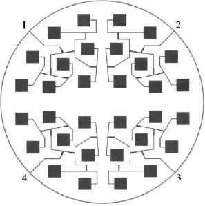
Figure 7.11. Four feed networks that comprise a 3-concentric-ring array.
A two-way divider requires R = 2Zc/3, while a three-way divider needs resistors of R = Zc/2.
Resistive divider efficiency decreases as N increases. The power transferred to each arm is 1/N2, which is much less than the 1/N of a lossless divider. Isolation in the resistive divider is equal to its insertion loss.
The Wilkinson power divider splits an input signal into two equal phase output signals or combines two equal-phase signals into one in the opposite direction [3]. It is lossless when all the output ports are matched. A diagram of a three port Wilkinson divider is shown in Figure 7.12. Quarter-wave transformers match ports 2 and 3 to port 1. The resistor (Rw) matches all ports and isolates port 2 from port 3 at the center frequency. Since the resistor adds no loss to the power split, an ideal Wilkinson divider is 100% efficient. A signal enters port 1 then splits into equal amplitude and phase signals at output ports 2 and 3. When the signals are recombined at port 3, they have equal amplitude and are 180° out of phase, since CCW signal travels half a wavelength further than the CW signal. The signals cancel at port 3. Since each end of the isolation resistor between ports 2 and 3 is at the same potential, no current flows through it, so it is decoupled from the input. The two output port terminations add in parallel at the input. In order to combine to Zc, a quarter-wave transformer is placed in each leg. If the quarter-wave lines have an impedance of ![]() , then the input is matched when ports 2 and 3 are terminated in Zc. Figure 7.13 is a picture of a three-port Wilkinson power divider. Note that this Wilkinson power divider has four stages. The four different width curves have different impedances designed to make it very wide band 0.5 to 4 GHz. This type of power divider can be extended to make an 8-to-1 power combiner (Figure 7.14). Its tree-like structure takes up a lot of room because it is very broadband.
, then the input is matched when ports 2 and 3 are terminated in Zc. Figure 7.13 is a picture of a three-port Wilkinson power divider. Note that this Wilkinson power divider has four stages. The four different width curves have different impedances designed to make it very wide band 0.5 to 4 GHz. This type of power divider can be extended to make an 8-to-1 power combiner (Figure 7.14). Its tree-like structure takes up a lot of room because it is very broadband.

Figure 7.12. Diagram of a three-port Wilkinson power divider.
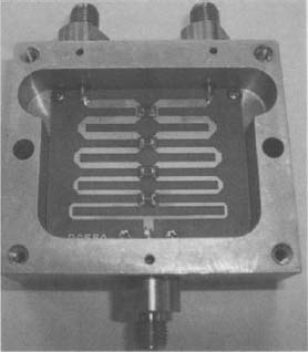
Figure 7.13. Picture of a three-port Wilkinson power divider.
So far, only corporate feeds that are based on a power of two have been presented. If the number of elements in the array is not a power of two, then power dividers with ratios other than 2:1 are needed. Also, when there is an amplitude taper, the power division needs to be unequal [6]. In order to make the unequal split, the quarter-wave sections must be of different impedances, to encourage more of the signal to travel into or out of the lower-impedance arm. In addition, a second set of quarter-wave sections are needed to transform the arm impedances back to 50Ω. This configuration looks similar to a two-stage Wilkinson without the second isolation resistor. The following set of equations ensure that all the ports are matched and ports 2 and 3 are isolated [7]:

Figure 7.14. Picture of an 8-to-1 Wilkinson power combiner.

Example. Design the feed network for a 4-element Chebyshev array with 20-dB sidelobes. The amplitude weights for the Chebyshev taper are
w = [0.5761 1.0 1.0 0.5761]
which equates to power at the elements of
P = [0.3319 1.0 1.0 0.3319]
![]()

Figure 7.15. Picture of a series feed for a linear microstrip antenna.
The elements of a series fed array all share the same transmission line/waveguide. An example is shown in Figure 7.15 of a single microstrip line that feeds a long line of rectangular patches. The microstrip line to an element taps the signal from the main microstrip line. A quarter-wave transformer with a mitered corner provides the match to the patch. A very common example of a series-fed array is the Hawk radar waveguide array shown in Figure 7.16. The signal enters the port, splits with half traveling up and the other half traveling down. Since the signal reaches the top and bottom waveguides first and the center waveguides last, the waveguides that tap the signal from the feed waveguide and wrap around to feed the slotted waveguide in the front of the array become increasingly shorter from top to bottom.
The array in Figure 7.17 is an example of a combination feed where the corporate feed distributes the signal to several series-fed patches. Some interesting corporate and series feeds can be found in reference 8.
A 32-element array of pyramidal horns with a corporate waveguide feed was designed to operate at 76.6 GHz [9]. The array measures 1.3 cm tall by 17.8 cm wide by 12.7 cm deep with horns that are 1.3λ (0.39 cm) in the H plane (array plane) and 2.0λ (0.79 cm) in the E plane. A 5-stage H-plane waveguide power divider uses equal power splits in stages 1 and 5 and unequal power splits in stages 2, 3, and 4 to produce a 40-dB Taylor distribution. Element spacing did not leave enough room for unequal power splitting in stage 5. Figure 7.18 shows the fields modeled inside the waveguide feed (right side only) with a blow-up of the 93:7 split at stage 3. The array was milled in two pieces—top and bottom—using numerical control techniques with very tight tolerances (Figure 7.19). Antenna patterns were measured at 76.3, 76.6, and 78 GHz as shown in Figure 7.20. The pattern at 76.6 GHz has the highest gain. A blow-up of this pattern appears in the upper right of the figure.

Figure 7.16. Picture of a series-fed Hawk radar waveguide array. (Courtesy of the National Electronics Museum.)

Figure 7.17. Picture of a corporate-series-fed microstrip array.

Figure 7.18. Picture of Fabricated Integrated Receive Array with the top half on the left and the bottom half on the right. (Courtesy of Amir Zaghloul.)

Figure 7.19. Array half with Taylor distribution power split of 93:7. (Courtesy of Amir Zaghloul.)
7.5. SLOTTED WAVEGUIDE ARRAYS
Cutting holes in a rectangular waveguide is a relatively simple way to create a series-fed linear array. The elements are typically narrow rectangular slots cut in the waveguide as shown in Figure 7.21. Slotted waveguide arrays are often used in place of reflector antennas, because they are very thin and are easily designed for low sidelobes. The Joint Surveillance Target Attack Radar System (Joint STARS) is a long-range, air-to-ground surveillance system designed to locate, classify, and track ground targets in all weather conditions.

Figure 7.20. Measured antenna patterns of the 32-element array of horns. (Courtesy of Amir Zaghloul.)

Figure 7.21. Slots cut into side of waveguide for the PAVE Mover antennas of Joint STARS. (Courtesy of Northrop Grumman and available at the National Electronics Museum.)

Figure 7.22. Equivalent circuit of a longitudinal slot array.
The E-8C, a modified Boeing 707, carries this phased-array radar antenna in a 26-foot canoe-shaped radome under the forward part of the fuselage [10, 11]. The antenna scans electronically in azimuth, and it scans mechanically in elevation from either side of the aircraft.
7.5.1. Resonant Waveguide Arrays
A waveguide terminated with a short has a standing wave with peaks that start λg/4 from the short and occur every λg/2 afterwards (see Chapter 4). The most common form of a resonant waveguide array has longitudinal slots in the broad face of the waveguide. The current on the waveguide wall reverses direction every λg/2 and flows in the opposite direction on either side of a centerline. In order to have consecutive elements in phase, they are placed λg/2 apart and offset on opposite sides of the centerline by Δn. Thus, these alternating offsets add an additional π radians of phase shift that compensates for the π radians of phase shift due to the λg/2 slot spacing in order to have all the slots radiate in phase. The offsets in a TE rectangular waveguide of cross section a × b are found from [12]

Figure 7.22 shows the equivalent circuit of a longitudinal resonant slot array with N conductances spaced λg/2 apart. Since the slots are spaced λg/2 apart, the input conductance to the array is the sum of all the normalized slot conductances.
Ideally, all the power input to the waveguide should be radiated through the slots. The power radiating from each slot should sum to one when the input power is normalized [13].

Figure 7.23. Diagram of the 6-element longitudinal slot array with a 20-dB Chebyshev taper.
A voltage V applied across slot n radiates the power
where an is the slot amplitude and K is a constant. As a result, an = gn, so the offsets are found from (7.19) for a desired amplitude taper.
Example. Find the slot offsets for a longitudinal offset slot resonant array of 6 elements with a Chebyshev taper having 20-dB sidelobes. Assume the array operates at 10 GHz. First, find the desired amplitude taper:
w = [0.5406 0.7768 1 1 0.7768 0.5406]
Then find K:
![]()
The conductances for each slot are found using (7.22):
g = [0.0771 0.1592 0.2638 0.2638 0.1592 0.0771]
Finally, the offsets are found from (7.20):
Δ1 = Δ6 = 0.2293
Δ2 = Δ5 = 0.3295
Δ3 = Δ4 = 0.4242
Since λn = 3.98 cm for a waveguide with dimensions 2.286 by 1.016 cm, the element spacing is λg/2 = 1.99 cm. Figure 7.23 is a diagram of the 6-element slot array design. The array has a gain of 13.9 dB, and the first sidelobe is 24.9 dB below the main beam (Figure 7.24).

Figure 7.24. Orthogonal cuts in the far-field pattern of the slot array in Figure 7.23.

Figure 7.25. As the frequency changes, the slots are not longer at the same position on the standing wave inside the waveguide.
A resonant slot array has a narrow bandwidth. As the frequency changes, the peaks of the standing wave move (dashed line in Figure 7.25). Thus, the field distribution in a slot changes more dramatically, the farther it is from the short. Long resonant slot arrays are narrowband because the impedance bandwidth is approximately equal to 50%/N [14].

Figure 7.26. Equivalent circuit of a longitudinal nonresonant slot array.
In general, the mutual coupling for longitudinal broadwall slots in a single waveguide (linear array) can be ignored. Sidewall slots have high mutual coupling, so more care must be taken when waveguides are stacked to make a planar array [15].
7.5.2. Traveling-Wave Waveguide Arrays
A traveling-wave slot array has an element spacing either greater than or less than λg/2. The waveguide ends in a matched load that reduces the reflections that causes the standing wave. The element spacing is chosen to create a beam at the angle θ = θS when ![]() = 0. Figure 7.26 shows the equivalent circuit of a longitudinal nonresonant slot array with N conductances spaced d apart. The slots are resonant (have real admittance) and the mutual coupling is negligible.
= 0. Figure 7.26 shows the equivalent circuit of a longitudinal nonresonant slot array with N conductances spaced d apart. The slots are resonant (have real admittance) and the mutual coupling is negligible.
The array factor when ![]() = 0 is
= 0 is
The main beam points at θs when
If θs is known, then the element spacing is found from (7.24):
If d is known, then θs is found from (7.24):
Assuming that only one beam is desired, the minimum spacing occurs when θs = −90° for m = 0 and the maximum occurs when a second main beam emerges at θs = −90° for m = 1 [12].
If d is known, then the scan angle is given by
The conductance of the resonant slots when q is the fraction of incident power dissipated in the matched load is given by
This works when N ≥ 12 and θs < 0.
As with the resonant waveguide array, all the power input to the waveguide should radiate through the slots. If the input power is normalized, then all the powers radiating from the slots should sum to one as in (7.21). If a voltage V is applied across slot n, then the power radiated by that slot is
where wn is the slot amplitude and K is a constant.
Example. Find the slot offsets for a longitudinal offset slot nonresonant array of 12 elements with an ![]() = 3 Taylor taper having 25-dB sidelobes. The main beam points at θs = −10° at 10 GHz.
= 3 Taylor taper having 25-dB sidelobes. The main beam points at θs = −10° at 10 GHz.
First, find the desired amplitude taper:
w = [0.3726 0.4693 0.6276 0.7957 0.9286 1.0000
1.0000 0.9286 0.7957 0.6276 0.4693 0.3726]
Then find K:
![]()
The power at each slot is
P = [0.0160 0.0254 0.0455 0.0731 0.0995 0.1154
0.1154 0.0995 0.0731 0.0455 0.0254 0.0160]

Figure 7.27. Diagram of a longitudinal slot array.
The conductances for each slot are found using (7.29):
g = [0.0160 0.0258 0.0474 0.0800 0.1185 0.1559
0.1847 0.1954 0.1783 0.1350 0.0872 0.0602]
Finally, the offsets are found from (7.20):
Δ = [0.1046 0.1328 0.1799 0.2337 0.2844 0.3262
0.3550 0.3651 0.3488 0.3035 0.2440 0.2028]
Assuming λg = 3.98cm, the element spacing for θs = 30° is
![]()
Figure 7.27 is a diagram of the 12-element slot array design.
Air-filled slotted waveguides have small scan angles in order to avoid grating lobes. Placing a dielectric inside the waveguide increases the scan range by decreasing λg, which in turn increases θs as calculated by (7.28).
So far, only the design of linear slot arrays has been described. Planar slot arrays are much more difficult, because the mutual coupling between parallel slots becomes significant. A good starting point is to design a linear slot array and stack them. This serves as an initial guess for a numerical optimization algorithm that will vary the offset and length of the slots to achieve the design goals [10].
The Airborne Warning and Control System (AWACS) uses an S-band planar slot array with over 4000 edge slots (Figure 7.28) to detect and track targets from the air [16]. It sits atop a Boeing 707 inside a radome (Figure 7.29). The radome and antenna rotate in azimuth at 10 revolutions per minute while the antenna uses 28 ferrite phase shifters to scan in elevation. Figure 7.30 shows the measured antenna pattern. The design goal for average side-lobe level was −37 dB while the actual measured average sidelobe level is −45 dB.

Figure 7.28. AWACS antenna array. (Courtesy of the National Electronics Museum.)

Figure 7.29. Picture of the AWACS in flight. (Courtesy of the US Air Force.)

Figure 7.30. Far-field pattern of AWACS antenna. (Courtesy of the National Electronics Museum.)
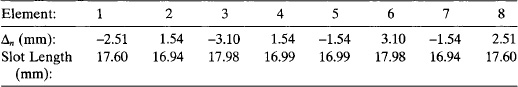
Example. In reference 10, the design of a 2 × 4 resonant slotted waveguide array is presented at 8.933 GHz. The waveguide is 23.5 mm × 3.12mm. Slot lengths and displacements are given in Table 7.1 when the slot width is 1.63 mm. A computer model of the array is shown in Figure 7.31 with the E- and H-plane pattern cuts in Figure 7.32.
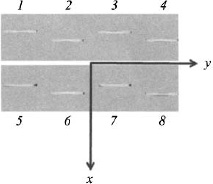
Figure 7.31. A 2 × 4 planar slot array.
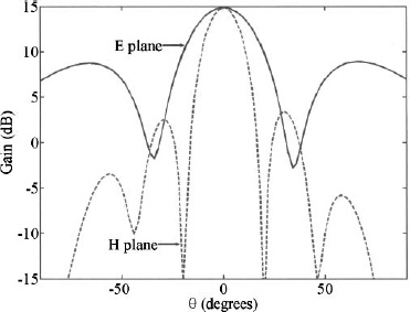
Figure 7.32. Orthogonal cuts in the antenna pattern of the 2 × 4 slot array.
TABLE 7.1. slot Characteristics for a 2 × 4 Planar Array
7.6. BLASS MATRIX
A Blass matrix ismultibeam feed network that has M beams created from N elements [17]. In a receive antenna, each beam port couples part of the signal from each element using a series feed line as shown in Figure 7.33. The couplers are equally spaced along the transmission line in such a way as to create a constant phase shift between elements in order to steer the beam to a desired angle. The beam and element transmission lines are terminated in matched loads. These terminations are needed to prevent reflections but have the unwanted side effect of reducing efficiency. If ψm,n is the phase length from beam port m to element n, then the phase difference between any two adjacent element is

Figure 7.33. Diagram of a Blass matrix.
This progressive linear phase shift steers beam m to an angle of
The Blass feed in Figure 7.33 is just one of many possible configurations [18].
7.7. BUTLER MATRIX
The Butler matrix [19] is a hardware version of the fast Fourier transform (FFT) [20] that was invented several years prior to the FFT. It transforms spatial signal samples taken by elements in a uniform linear array to samples in angular space which correspond to peaks of the main beams of array factors. A Butler matrix has N = 2M beam ports and N = 2M element ports that are interconnected via passive four-port 3-dB quadrature hybrid power couplers and fixed phase shifts.

Figure 7.34. Computer model of a 3-dB quadrature hybrid coupler or two-port Butler matrix.
The simplest version of a Butler matrix is also better known as a 3-dB quadrature hybrid coupler. The 3-dB quadrature hybrid coupler is a four-port device with two inputs and two outputs [3]. An input signal splits equally between the two outputs, but one of the outputs has a 90° phase shift due to the additional distance it has to travel. Figure 7.34 is a computer model of a 3-dB quadrature hybrid in microstrip. If antennas were attached to port 3 and 4, then an input signal, V1, at port 1 results in an output at port 4 of V1/![]() and at port 3 of − jV1/
and at port 3 of − jV1/![]() . An input signal at port 2, V1, results in an output at port 4 of − jV2/
. An input signal at port 2, V1, results in an output at port 4 of − jV2/![]() and at port 3 of V2/
and at port 3 of V2/![]() . The total signals at ports 3 and 4 are
. The total signals at ports 3 and 4 are

Figure 7.35 and Figure 7.36 show the amplitude and phase of the coupling coefficients as a function of frequency. At the design frequency of 6 GHz, the two ports receive equal signal amplitude but are 90° out of phase.
Larger Butler matrixes have N = 2m, m = 1,2, ..., input and output ports. The N beams are evenly spaced in angle such that each array factor beam n has a progressive linear phase shift given by
Therefore, the beam peaks occur when

Figure 7.35. Amplitude of the coupling coefficients vs. frequency for the hybrid coupler in Figure 7.34.
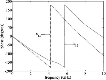
Figure 7.36. Phase of the coupling coefficients versus frequency for the hybrid coupler in Figure 7.34.
Since this is a uniform array factor, the peak sidelobes of each of the patterns are at about 13.2 dB. The angular coverage (bandwidth) is the angular separation between the two outer beams [21].

Figure 7.37. Diagram of a four-port Butler matrix.
The beam crossover level is found by substituting (7.36) into (7.35) to get
which is approximately 2/π when N is large. The orthogonal beams overlap at the −3.9-dB level and have the full gain of the array.
A basic component of the FFT is the twiddle factor, W. The twiddle factor equates to a constant phase shift defined by the steering phase difference between two adjacent elements.
The array factor at port m of an N element uniform linear array along the x axis is given by
where sn is a sample of the incident plane wave at element n. Large Butler matrixes are lossy, but diagrams of up to 32 elements are shown in the literature [18]. Outputs can be combined to form beams, and amplitude tapers can be placed on the elements [22].
Example. Design a 4-element Butler matrix and plot the beams for uniform and low-sidelobe tapers.
Figure 7.37 is a diagram of the Butler matrix with λ/2 element spacing. Figure 7.38 is a plot of the 4 beams using a uniform amplitude taper and (7.39).

Figure 7.38. The four beams associated with the four-port Butler matrix.

Figure 7.39. Butler matrix with amplitude taper.
An element amplitude taper of produces the low-sidelobe beams shown in Figure 7.39.
7.8. LENSES
A waveguide lens antenna consists of a feed placed at the focal point of a lens made from stacking waveguides. The shape of the lens and the length of the waveguides are such that the phase path from the focal point to the front end of the waveguide is a constant. Since the phase velocity is higher inside the waveguide, the lens has the opposite curvature of a typical dielectric lens. Figure 7.40 is the zoned waveguide lens antenna for the Nike AJAX MPA-4 radar. By 1956,80 Nike Ajax anti-aircraft missiles were deployed in the United States. An unconstrained lens [23] has curvature in the E plane (assuming linear polarization), while a constrained lens has curvature in the H plane. The unconstrained lens obeys Snell’s law on transmit and focusing occurs in the plane of the electric field. The constrained lens does not obey Snell’s law and focusing occurs normal to the electric field [24]. Thus, the signal radiated from each open-ended waveguide element has the same phase. Two more advanced versions of the waveguide lens are the Bootlace and Rotman lenses. These types of lenses are not limited to open-ended waveguides as elements [25].

Figure 7.40. Stepped waveguide lens antenna for the Nike AJAX MPA-4 radar. (Courtesy of the National Electronics Museum.)
7.8.1. Bootlace Lens
The bootlace lens consists of two back-to-back arrays with elements facing in opposite directions (Figure 7.41) [26]. An element on one side is connected to an element on the other side through a transmission line, phase shifter, amplifier, and so on. The elements on one side of the lens receives from/ transmits to a feed placed at the focal point. The shape of the input and output arrays, the length of the transmission lines between the input and output elements, and the amplitude and/or phase weights between the receive and transmit elements determine the performance of the lens. Transmission lines in the lens are not as limited in length as are the waveguides in a waveguide lens. Thus, a bootlace lens can be designed to have an on-axis focal point like the waveguide lens, but it will also have two conjugate focal points. The feed has either one antenna placed at a focus or multiple antenna (multiple beams) placed along a focal arc. Gent found that the if the lens has a radius of 2R, then the focal points lie on a circle having radius R [27]. A basic single-beam bootlace lens has one antenna at the feed, and the lens has a spherical shape on the side facing the feed and a flat face on the opposite side.

Figure 7.41. Diagram of the bootlace lens.
If the side of the lens facing the feed has a spherical shape while the other side has a flat face, then equal length transmission lines between the elements on the two faces produce a plane wave output. Since the transmission lines are the same length, it is independent of frequency. This lens can have up to 4 focal points that are symmetric about the lens axis. A feed placed on a curve that runs through these focal points will result in reasonably focused beams. Perfect focus only occurs when the feed is placed at one of the focal points. It is possible to extend the design of a bootlace lens to three dimensions [25]. The Patriot radar, AN/MPQ-53, is a space-fed array approximately 2.5 m in diameter with over 5000 elements (Figure 7.42) [28]. Elements in front of the array are circular waveguides that are dielectrically loaded. They are connected to the rear rectangular waveguide dielectrically loaded via a ferrite phase shifter. Its feed consists of horns that are 2.5 m in back of the array.
7.8.2. Rotman Lens
A Rotman lens [29] is a type of bootlace lens with three focal points. It forms simultaneous multiple beams for an antenna array as shown in Figure 7.43. M elements at the beam ports (xbm, ybm) are placed on a curved arc. They radiate to or receive from the curved back of the lens. The elements along the curved portion of the lens are at the array ports (xpn, ypn). Array elements are placed along the outside portion of the lens along a straight line (xn, yn). Each beam port creates one array factor from the array elements. The beams have their peaks steered to predetermined angles based on the geometry. Because it has no moving parts or phase shifters it offers an inexpensive alternative to corporate feed networks. The Rotman lens is very broadband, unlike the Butler matrix. A switching mechanism at the output can be used to select the appropriate beam in the desired look direction. In addition, interpolation can be used in direction finding to locate signals between adjacent beams.
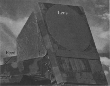
Figure 7.42. Patriot radar lens antenna array. (Courtesy of Raytheon Company.)
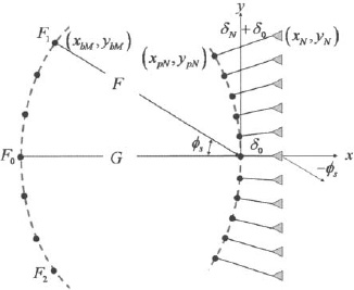
Figure 7.43. Diagram of a Rotman lens.
The original design equations for the Rotman lens appeared in reference 29. These equations have been modified to include the permittivity of the lens substrate and the permittivity of the transmission lines and are given by [30]
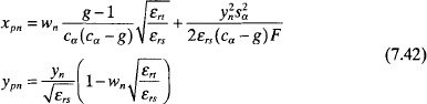
where
N = number of array ports and elements
M = number of beam ports
d = element spacing
g = G/F
cα = cos α
sα =sin α
= relative dielectric constant of substrate
= relative dielectric constant of transmission lines


The original paper has an error in the B term which has unfortunately propagated through some papers published in the literature. These equations assume the lens feeds an N-element uniform linear array. There are M feed ports that are placed along a circular arc of radius R. The M beams point at the angles γm which are measured from broadside. Transmission line lengths inside the lens are found from wn.
where δ0 is the smallest length at the center of the lens.
Example. Find the locations for the point sources for a Rotman lens with G = 4.24, F = 4, d = 0.6, α = 30°, Nbeam = 7, N = 11, ![]() = 1,
= 1, ![]() = 1, and δ0 = 0.
= 1, and δ0 = 0.
Substituting these values into (7.41), (7.42), and (7.43), results in the design shown in Figure 7.44. The locations of the ports and elements are in Table 7.2.
Figure 7.45 is the design of an 8-beam Rotman lens with 8-element ports at a center frequency of 10 GHz. The matched loads on the sides absorb power incident on them in order to reduce unwanted reflections. This design was then implemented in microstrip as shown in Figure 7.46. Array elements are connected to the SMA connectors on top while receivers are connected to the beam ports. Matched loads are placed on the side SMA connectors to reduce internal reflections.

Figure 7.44. Rotman lens design with corresponding array factors.
TABLE 7.2. Element and Port Locations in λ for the Rotman Lens Design
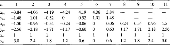

Figure 7.45. Computer design of a Rotman lens [31].
An array that has a full 360° azimuth coverage can be made around a polygon or circle as described in Chapter 5. Beam scanning with these structures is accomplished by a commutating feed and/or beam scanning. An alternate approach uses a Rotman lens that has overlapping beams covering all azimuth angles [32]. Figure 7.47 is a diagram of the concept applied to a square having 4 elements on each side. Every other port in the Rotman lens is a beam port while the other half are connected to the elements. In order to work, the focal arc and the curvature of the inside of the lens must be identical. A switching network connects the desired beam to the receiver. This concept can be extended to an array with more faces as shown in Figure 7.48b or to a circular array as in Figure 7.48c. Figure 7.49 is an experimental prototype of a 360° Rotman lens for a square array with 6 elements per face.
7.9. REFLECTARRAY
Reflect arrays are a cross between a reflector antenna and an antenna array. The feed antenna transmits to/receives from a flat to slightly curved surface covered with radiating elements as shown in Figure 7.50. Radiating elements are open-ended waveguides, patches, dipoles, and so on. The elements focus the signal at the feed for receive or in the far field for transmit. Element type, orientation, and size determine the phase and/or polarization of the reflected signal. The first reflectarray used shorted rectangular waveguides [33] whose length determined the signal phase shift. These waveguide reflectarrays were too heavy to be practical. Reflectarrays became much more practical when they were made from printed elements.

Figure 7.46. Experimental microstrip Rotman lens. (Courtesy of Pennsylvania State University.)

Figure 7.47. The beam and element ports are interleaved. (Courtesy of Amir Zaghloul.)
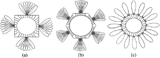
Figure 7.48. 360-degree Rotman lens designs, (a) Four sides, (b) Six sides, (c) Circular.
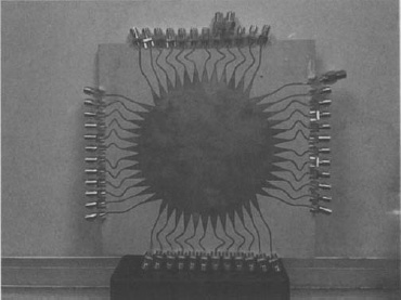
Figure 7.49. Experimental four-sided 360° Rotman lens. (Courtesy of Amir Zaghloul.)
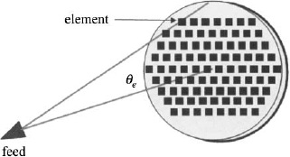
Figure 7.50. Diagram of the spatial phase delay of a reflectarray.
Like a parabolic reflector, the reflect array has a very high efficiency, because it avoids lossy power dividers. Unlike the reflector, the main beam of the reflect array can be steered to large angles from broadside. The disadvantage of the reflect array is that it is narrowband. Bandwidth is limited by both the elements and the differential phase delay. The differential phase delay can be reduced as follows [34]:
- Reduce the size of the reflecting surface.
- Increase the distance of the feed from the reflecting surface.
- Curve the reflecting surface.
- Use time delays instead of phase shifts at the elements.
Aperture efficiency is found from [34]
As with reflector antennas, there is also a spillover efficiency given by
where θe is the angle between feed normal and line from feed to array edge, and cosq θ is the feed element pattern.
The RARF (Reflected Array Radio Frequency) used in the AN/APQ-140 Radar was manufactured by Raytheon in 1969 [35]. It has 3500 phase shifting modules that work for any polarization (Figure 7.51). Electronic phase controls allows ±60° scanning in elevation and azimuth. This is a passive array with no gain in the modules.
7.10. ARRAY FEEDS FOR REFLECTORS
Phased array feeds have better illumination control of a reflector surface than does a single antenna element. This control aids in beam steering [36], adaptive nulling [37], beam shaping [38], and generating multiple beams [39]. Large arrays have more degrees of freedom to shape the pattern; but as the size of the array increases, the feed blockage and weight increases as well. The array pattern of a large uniform array has a narrow main beam that only illuminates a small portion of the reflector. In order to maximize antenna gain, the reflector is calibrated by adjusting the phase of the elements in the feed array. A circular planar array feed with triangular spacing has been used to compensate for spherical reflector aberrations using a mean square minimization technique [40]. Approaches to synthesizing phased array weights to maximize gain usually assume perfect analog array weights. Closed-form solutions for the array feed excitations exist that optimize the directivity of an ideal offset reflector [41]. Compensating for reflector surface distortions improves the main beam gain as well as the sidelobe levels [42].
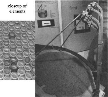
Figure 7.51. Picture of RARF reflectarray. (Courtesy of the National Electronics Museum.)
An array at the focal point of a front-fed reflector causes blockage that severely degrades the main beam of the reflector antenna. It is possible to adjust the phase shifters of the elements using a genetic algorithm until the maximum reflector gain is obtained at ![]() = 0° [43]. Optimizing the amplitude taper of the feed array contributes very little to the calibration, so it is ignored. Consider a 5-element uniform array with elements spaced half a wavelength apart placed at the focal point of a two-dimensional parabolic cylinder reflector with a diameter of 20λ and a focal distance of 10λ (F/D = 0.5). Its geometry with the compensated and uncompensated feed patterns appear in Figure 7.52. Compensated and uncompensated reflector antenna far-field patterns are shown in Figure 7.53. Calibration increases the main beam at
= 0° [43]. Optimizing the amplitude taper of the feed array contributes very little to the calibration, so it is ignored. Consider a 5-element uniform array with elements spaced half a wavelength apart placed at the focal point of a two-dimensional parabolic cylinder reflector with a diameter of 20λ and a focal distance of 10λ (F/D = 0.5). Its geometry with the compensated and uncompensated feed patterns appear in Figure 7.52. Compensated and uncompensated reflector antenna far-field patterns are shown in Figure 7.53. Calibration increases the main beam at ![]() = 0° by 4.7 dB and lowers the sidelobes adjacent to the main beam by 0.8 dB.
= 0° by 4.7 dB and lowers the sidelobes adjacent to the main beam by 0.8 dB.
Using an offset reflector reduces feed blockage, but the array still needs calibration for small F/D to ensure maximum gain at ![]() = 0°. An offset reflector with an F/D of 0.8 places the feed about 10λ from the reflector surface. At this F/D ratio, a uniform array works well, and the angle of the feed is not very sensitive. Reducing the F/D to 0.3 brings the feed much closer to the reflector surface and necessitates calibration. Calibration for the offset feed includes adjusting the tilt or pointing direction of the feed. Figure 7.54 shows the antenna patterns of the calibrated and uncalibrated offset reflectors. Calibration provides a 4-dB improvement to the main beam at boresight.
= 0°. An offset reflector with an F/D of 0.8 places the feed about 10λ from the reflector surface. At this F/D ratio, a uniform array works well, and the angle of the feed is not very sensitive. Reducing the F/D to 0.3 brings the feed much closer to the reflector surface and necessitates calibration. Calibration for the offset feed includes adjusting the tilt or pointing direction of the feed. Figure 7.54 shows the antenna patterns of the calibrated and uncalibrated offset reflectors. Calibration provides a 4-dB improvement to the main beam at boresight.

Figure 7.52. Calibrated and uncalibrated 5-element phased array feed for the reflector antenna.

Figure 7.53. Front-fed reflector far-field patterns when the 5-element array feed is calibrated and uncalibrated.

Figure 7.54. Offset-fed reflector far-field patterns when the 5-element array feed is calibrated and uncalibrated.
7.11. ARRAY FEEDS FOR HORN ANTENNAS
Many systems need high-gain antennas that electronically scan over a limited angular range, although the range may be several hundreds of beamwidths. Large, array-fed reflectors are high gain but have a scan that is limited to several tens of beamwidths. Large conventional arrays are high gain and capable of scanning over a large angular extent but are prohibitively expensive due to the large number of elements. A hybrid array-fed horn antenna is a viable and affordable alternative to full phased array antennas for applications such as space-based radar. The minimum number of elements in an array is given by [44]
where Ωs is the solid scan angle (field of view) and θ3dB is the array beamwidth. Dividing the number of elements in an array by Nmin gives the element use factor [21]. For a scan sector of 60° or more, the element use factor is close to unity. If the scan is limited to ±20°, the planar array element use factor is very high, and conventional phased arrays with one control per element over a full aperture are not very efficient.
Figure 7.55 explains how the hybrid reflector-array antenna uses the Winstone Cone light concentrator to funnel all wavelengths passing through the entrance aperture out through the exit aperture to a planar array feed [45]. The two side reflectors were optimized for maximum ray intercept over the prescribed angular range [46]. Off-axis rays hitting the reflectors take multiple bounces before they reach the feed array. Reflectors are shaped so that incident waves within a ±20° sector only bounce once before reaching the feed array.

Figure 7.55. Diagram of the array-fed horn antenna. (Courtesy of Boris Tomasic, USAF AFRL.)
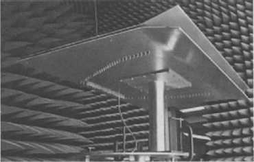
Figure 7.56. Picture of the experimental array-fed horn antenna. (Courtesy of Boris Tomasic, USAF AFRL.)
A 43-element feed with d = 0.45λ0 at 10 GHz with 20% bandwidth was built for a parallel-plate flared waveguide shown in Figure 7.56 [44]. A diagram of the element probes and reflector outline appears in Figure 7.57. The parallel plates are separated by 0.37λ0, and the probe height is 0.23λ0. The antenna aperture is 40λ0 (1.2m), while the array feed is 20λ0 (0.6m). If the array scans ±20°, then the array element spacing must be less than 0.7λ. If the array is 1.2 m long, then it would have 57 elements. Thus, the array-fed horn antenna has an element use factor of 43/28 = 1.53, which is better than the full array use factor of 54/28 = 2.03 [44].

Figure 7.57. Diagram of the elements and array-fed horn antenna. (Courtesy of Boris Tomasic, USAF AFRL.)

Figure 7.58. Plots of the calculated and measured far field pattern of the array-fed horn antenna at broadside. (Courtesy of Boris Tomasic, USAF AFRL.)
The array-fed horn antenna was modeled on a computer using physical optics (PO), and the experimental antenna was measured in an anechoic chamber. Figure 7.58 shows that the measured and computed far-field patterns agree well within θ = ±30°. No grating lobes appear when the beam is steered to θs = −20° (Figure 7.59).

Figure 7.59. Plots of the calculated and measured far field pattern of the array-fed horn antenna at θs = −20°. (Courtesy of Boris Tomasic, USAF AFRL.)
All the element patterns were calculated using the uniform theory of diffraction (UTD) and compared with measured element patterns (Figure 7.60 has four examples). Agreement is quite good over θ = ±90°. An accurate representation of the far-field pattern is obtained using the measured far-field element patterns in the 43-element array as was done in Chapter 6. The amplitude and phase weights (Figure 7.61) were found that limit the maximum sidelobe level to below 30 dB using the method of alternating projections [47]. Figure 7.62 is the resulting far-field pattern.
7.12. PHASE SHIFTERS
Phase shifters change the phase of a signal in a transmission line or waveguide by inducing a phase delay between 0° and 360° (in time delay terms, between 0 and λ/c). Ideally, the amplitude of the signal passing through the phase shifter is the same for all phase states. Some phase-shifting technologies have a high insertion loss and must be integrated with an amplifier to be useful. Most phase shifters are designed to be reciprocal (even when they use nonreciprocal components), in order to have identical characteristics in the transmit and receive modes. Phase shifters used in phased arrays must have digital interfaces (including those that use analog technology to cause the phase delay), so they can be computer-controlled. Phase shifters work by either forcing the signal to take a longer/shorter path or increasing/decreasing the phase velocity over a set distance.
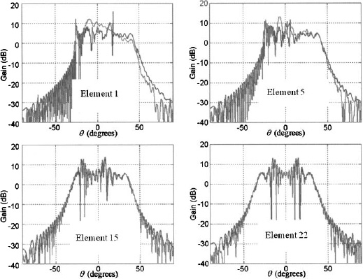
Figure 7.60. Plots of the calculated and measured far field element patterns of the array-fed horn antenna. (Courtesy of Boris Tomasic, USAF AFRL.)

Figure 7.61. Low sidelobe element weights synthesized using the measured element patterns. (Courtesy of Boris Tomasic, USAF AFRL.)
Switched line phase shifters add line lengths to increase the phase of a signal. When bit n of an N-bit phase shifter is a 1, the signal is delayed by traveling an additional 180°/n in phase. Thus, a three-bit phase shifter with input [1 1 0] has an additional phase delay of 270° (see Figure 7.63). Switches are fast and lightweight but have low power-handling capability and are possibly lossy. A number of different type of switches used in phase shifters technology include PIN diode and MEMS (micro-electromechanical systems).

Figure 7.62. Low-sidelobe patttern using the measured element patterns and the synthesized weights. (Courtesy of Boris Tomasic, USAF AFRL.)

Figure 7.63. Diagram of a switched line phase shifter.
The PIN diode has heavily doped p-type and n-type regions separated by an intrinsic region [3]. A forward bias results in a very low resistance to high frequencies, while a reverse bias acts like an open circuit with a small capacitance. PIN diodes have a low frequency limit of about 1 MHz due to carrier lifetime. A few milliamps of DC current can cause the PIN diode to switch one or more amps of RF current. These switches have the disadvantage of being current controlled rather than voltage controlled.
MEMS switches have low losses, high isolation, high linearity, small size, low power consumption, and low cost and are broadband. On the other hand, they tend to have high losses at microwave and millimeter waves, limited power-handling capability (~100mW), and they may need expensive packaging to protect the movable MEMS bridges against the environment 16]. An example of an RF MEMS switch developed by Radant Technologies is shown in Figure 7.64 [48]. The base of the cantilever beam connects to the source to its right. The free-standing tip of the beam suspends above the drain. An electrostatic force pulls the beam down when a voltage is applied to the gate. Closing the switch results in an electrical path between the beam and the drain. MEMS switches have high isolation when open, but they have low insertion loss when closed while consuming a small amount of power. At first, MEMS switches had low reliability, but recent advances have made them competitive with other technologies.

Figure 7.64. Picture of a Radant MEMS switch.(Courtesy of Radant Technologies, Inc.)
Ferrite phase shifters use current to magnetize or demagnetize a piece of ferrite in a waveguide [3]. When it is demagnetized, the phase is zero. When it is magnetized, the phase is a function of the length of the ferrite. Ferrite phase shifters are reciprocal when the variable differential phase shift through the device is the same in either direction. A latching phase shifter makes use of the hysteresis curve for a ferrite. A current pulse controls whether the ferrite is in the positive or negative saturation state. The length of the ferrite is chosen so that the desired differential phase shift between the two saturation states corresponds to phase bit n where the phase for bit n is 360°/2n. A phase shifter has independently biased ferrite sections of decreasing size in series. Latching ferrite phase shifters have the advantage of not requiring a continuous bias current and have been made from about 2 GHz to 94 GHz [49].
TABLE 7.3 Phase Shifter Characteristics [16]

The rotary-field phase shifter, on the other hand, induces a phase shift by rotating a fixed amplitude magnetic bias field [49]. It is inherently low phase error since the phase shift is controlled by the angular orientation of the bias field rather than the magnitude of the bias field. The angular orientation is a function of the current fed to a pair of orthogonal windings. Rotary-field phase shifter operate from S-band through Ku-band (2–18 GHz).
Ferroelectric materials have a tunable dielectric constant. For phase shifters made from a ferroelectric material like barium strontium titanate (BST), part or all of the substrate of the phase shifting circuit is made from ferroelectric material [50]. As the fields pass through the ferroelectric layer, the phase velocity can be controlled by changing the permittivity of the ferroelectric [51].
Table 7.3 lists the characteristics of several types of phase shifters. Ferroelectrics and MEMS dominate the low cost. Ferrite phase shifters are needed for high-power applications, but also consume a lot of DC power consumption. Ferrites and MEMS tend to have slow switching speeds.
Figure 7.65 is a picture of a waveguide-fed linear array of slots. Parts on the left are assembled to make the array on the right. The phase shifters fit between the waveguide feed and the slots. Electronic controls lie on top of the phase shifters.
7.13. TRANSMIT/RECEIVE MODULES
The transmit/receive (T/R) module has five functions [52]:
- Amplify the transmit signal.
- Amplify and provide low-noise figure for the receive signal.
- Switch between transmit and receive mode.
- Phase control of transmit and receive signals.
- Protect low-noise amplifier.

Figure 7.65. Diagram of a linear slot array with phase shifters. (Courtesy of Northrop Grumman and available at the National Electronics Museum.)

Figure 7.66. Diagram of a T/R module.
A diagram of a T/R module is shown in Figure 7.66 [53]. The phase shifter at the bottom of the T/R module performs beam steering and calibration. A circulator or switch at either end isolates the transmit and receive channels. Communications systems usually operate in full duplex mode (simultaneously transmit and receive), while radar systems usually operate in half-duplex mode (sequentially transmit and receive). Care must be taken to isolate the transmit and receive channels, as well as protect the transmit amplifier from reflections that result from impedance mismatches while beam scanning. An attenuator appears in both paths in order to calibrate the paths and implement lowsidelobe tapers. The attenuator only reduces gain, so the gain at each element starts at the minimum attenuation and is adjusted down rather than set at the mean level and adjusted up or down. Attenuators throw away signal power and create heat, so they need to be applied wisely to avoid overheating and loss of signal power. The receive channel typically has 10–20 dB of gain from the low-noise amplifier (LNA) in order to establish a low-noise figure before phase shifting and traveling through the feed network. Power amplifiers in the transmit channel typically have about 30 dB of gain in order to compensate for the losses in the feed network [53].
Module calibration ensures desired performance at each element [53]. Ideally, when calibrating the array, the phase shifter’s gain remains constant as the phase settings are varied, but the attenuator’s insertion phase can vary as a function of the phase setting. In this situation, the calibration process only has to be done at the broadside beam location. The first step of this calibration process adjusts the attenuators for uniform gain at the elements. The phase shifters are then adjusted to compensate for the insertion phase differences at each element. Steering the beam just adds a linear phase shift to the calibration phase. This calibration should be done across the bandwidth and range of operating temperatures. If the phase shifter’s gain varies as a function of setting, then the attenuators need to be compensated as well. The process of adjusting the phase and amplitude iterates until the error is minimized. All the calibration settings are saved and applied at the appropriate times.
The transmitter feeding a T/R module can be either centralized at the array or subarray output or distributed at each element. Centralized power amplification has the following disadvantages [52]:
- The insertion loss of the beamformer and phase shifters occurs after the transmit amplifier or before the receiving amplifier. These losses degrade the array’s output power and noise figure. Attenuators also degrade a centralized system’s output power and noise figure.
- The power-handling requirement for centralized phase shifters and attenuators is significantly higher than a distributed system.
- A centralized amplifier conveys the same phase noise to each antenna element, creating correlated errors in the aperture.
- If the amplifier is a single device, then its failure will lead to failure of the phased array. A centralized amplifier can be made by power combining several lower-power amplifiers to minimize the impact of a single amplifier’s failure.
- Output power and efficiency degradation created by the insertion loss of the output power combiner is a significant drawback for solid-state centralized amplifiers.

Figure 7.67. Picture of the MERA T/R module. (Courtesy of the National Electronics Museum.)
The main disadvantage of distributed T/R modules is the increased cost and complexity associated with niters for reducing electromagnetic interference (EMI) [52]. In a centralized system, only one EMI filter is required and does not have the size restriction of fitting behind an element. Distributed amplification requires a filter for every T/R module. Distributed filtering typically has higher insertion loss than centralized filtering due to packaging size restrictions. The filter’s loss may degrade system noise figure and output power depending on its location in the array.
T/R module development started in 1964 with the Molecular Electronics for Radar Applications (MERA) Program [54]. A photograph of the brick module including the radiating element (dipole) is shown in Figure 7.67. The monolithic microwave integrated circuit (MMIC) was fabricated on high-density alumina and high-resistivity silicon, using thin-film techniques. Circuits are located on both sides of the module. The side shown in the photograph contains a four-stage S-band transmit amplifier at 2.25 GHz. The amplifier is followed by a times four frequency multiplier plus filters in order to transmit the 9-GHz signal. Also shown in the upper left-hand corner is a balanced mixer and a 500-MHz lumped element IF amplifier. Located on the opposite side is the four-bit phase shifter and local oscillator network. Each module in the array transmitted a peak power of 0.6 W at 9.0 GHz. A noise figure of 12 dB was obtained with a gain of 14 dB. The received signal is output from the module at 2.125 GHz. The module is 7.1 × 2.5 × 0.8 cm, and it weighs 0.95 ounces. A T/R switch was to be used at X band to separate the transmitter and receiver functions.
In 1987, the Advanced Tactical Fighter (ATF) program started the use of GaAs, MMIC technology in order to reduce the size and cost of T/R modules (Figure 7.68) [55]. The AN/APG-77 radar antenna is a phased array with 2000 T/R modules capable of scanning 120 degrees.
As MMIC and heat dissipation technology improved, arrays using many T/R modules migrated from a brick design to a tile design. Figure 7.69 is a diagram of one tile in a 17-GHz three-tile multibeam active array that was launched into geostationary orbit in 2008 [56]. Each tile has 33 RF modules, 16 low-noise amplifiers, a tile controller, and a power supply. The element spacing is one inch, with each element having a directivity of 14.4 dBi. A 2 × 2 subarray of helical elements are connected to a 4-to-1 combiner. A plot of the antenna pattern for the tile is shown in Figure 7.70. Steering to the maximum scan angle of 5° results in the pattern shown in Figure 7.71.
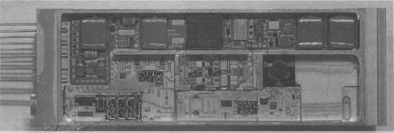
Figure 7.68. Picture of the ATF T/R module. (Courtesy of the National Electronics Museum.)

Figure 7.69. Example of an 8 × 8 array tile. (Courtesy of the Lockheed Martin, Corp. E. Lier and R. Melcher, A modular and lightweight multibeam active phased receiving array for satellite applications: Design and ground testing, IEEE Antennas Propagat. Mag., Vol. 51, No. 1, 2009, pp. 80–90.)
T/R modules have not enjoyed the mass production of other commercial technologies until recently. Computer, wireless, and solar cell initiatives are pushing substrate manufacturing that benefit T/R module design. Figure 7.72 is a diagram of power-handling capability of different T/R module substrates versus frequency [53, 57]. Gallium nitride (GaN) and silicon carbide MMIC chips have the potential to increase the T/R module power by one or two orders of magnitude. SiC technology offers 1–10 kW in the low-GHz frequency band with better thermal concuctivity than GaAs. GaN modules work from a little less than 10 kW below 10 GHz to a little less than 100W above 100 GHz. It is capable of reduced chip size, broad bandwidth, and higher operating voltage. SiGe and CMOS offer low-power, low-cost, high-performance T/R modules.

Figure 7.70. Predicted and measured antenna patterns of the tile when the main beam points at broadside. (Courtesy of the Lockheed Martin, Corp. E. Lier and R. Melcher, A modular and lightweight multibeam active phased receiving array for satellite applications: Design and ground testing, IEEE Antennas Propagat. Mag., Vol. 51, No. 1, 2009, pp. 80–90.)
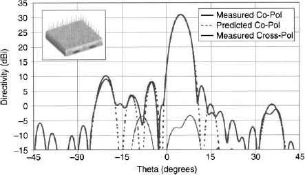
Figure 7.71. Predicted and measured antenna patterns of the tile when the main beam points at 5°. (Courtesy of the Lockheed Martin, Corp. E. Lier and R. Melcher, A modular and lightweight multibeam active phased receiving array for satellite applications: Design and ground testing, IEEE Antennas Propagat. Mag., Vol. 51, No. 1, 2009, pp. 80–90.)

Figure 7.72. Solid state power handling versus frequency for several substrate materials.
7.14. DIGITAL BEAMFORMING
Digital beamforming (DBF) [58, 59] is similar to the use of T/R modules, except the T/R module contains an analog-to-digital (AD) converter that outputs a digital signal directly to the computer. It has the advantages of improved dynamic range, ease of forming multiple beams, adaptive nulling, and low sidelobes. Like T/R modules, the AD converter can be either centralized or distributed [16]. The corporate feed in Figure 7.73a performs analog beamforming and converts the signal to digital once all the signals are combined. Figure 7.73b converts the analog signals to digital signals at each element. Figure 7.73c shows an array architecture in which the subarrays perform analog beamforming and the signals from the subarrays are converted to digital signals. This approach can increase the bandwidth of the array through digital time delay instead of hardware time delays. DBF is frequently implemented at the subarray level because the digital receivers are expensive, large, and heavy and require calibration. A full DBF array has the most flexibility and the least amount of feed hardware, because all weighting and combining is done in software. Calibration of the DBF can be done by coupling a calibration signal into the feed line from the element (Figure 7.74) [60]. Calibration can also be done using near-field or far-field sources [61]. Compensation for the amplitude and phase errors can be done in software. DBF is expensive and requires a lot of space behind each element, so it is usually limited to small arrays. DBF systems are moving up in frequency and becoming more common [62].

Figure 7.73. Digital beamforming versus corporate feed. (a) Corporate feed. (b) Subarray corporate feed and digital beamforming at the subarray ports. (c) Digital beamforming at each element.
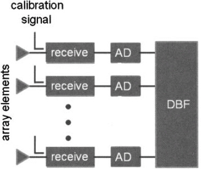
Figure 7.74. Diagram of a digital beamforming array.

Figure 7.75. Diagram of a neural beamforming array.
7.15. NEURAL BEAMFORMING
An artificial neural network is ideally suited to form beams given the signals at each element of an array. Unlike traditional beamforming algorithms, which require either extremely well-matched channels or extensive calibration, the neural network beamformer is trained in situ and learns to perform the required function regardless of array element degradations, large manufacturing tolerances, or scattering from the platform. The neural beamformer architecture consists of antenna measurement input preprocessing, an artificial neural network, and output postprocessing (Figure 7.75). In some special cases, the neural beamformer is similar to a Butler matrix [63].
The input nodes receive preprocessed antenna data that are sent to hidden layer (or Gaussian processing) nodes. Element signals, x1 = (x11, xl2, …, xln), l = 1, 2, …, L, are measured over the antenna field of view (±60°). Each element signal vector contains seven phase differences between adjacent elements in the array. The hidden layer of nodes have Gaussian activation functions. A processing node has an output that depends on the radial distance between the element signal vector and the node center, as well as on the spread parameter, σ. When the network receives the element input vector, the output of hidden layer node i is ![]() [64]:
[64]:
where i = 1, 2, …, q for q hidden layer nodes. An interpolation matrix, Φ, contains the processing node outputs, ![]() . Row 1 of this matrix is the outputs of the q hidden layer nodes corresponding to input vector xl.
. Row 1 of this matrix is the outputs of the q hidden layer nodes corresponding to input vector xl.
The output matrix, Y, has components ylj that are a weighted sum of the hidden layer outputs.
where j = 1,2,…, r for r output nodes and wij are the components of the weight matrix, W. The weights come from training the network on a subset of the L measured input vectors.
An 8-element array is trained using r = 13 output nodes, centered at 10° intervals from −60° to 60°. If the AOA (angle of arrival) is between two training angles, the nodes have an output between 0 and 1. The AOA, θ, for a wave between nodes j and j + 1, is found from [65]
where θj is the training angle for node j, and yj and yj+1 are the node output values produced by the network at nodes j and j + 1, respectively.
The network is trained using supervised learning (the network receives input vectors and the corresponding desired outputs), and backpropagation is used to find the weights.
After training, the desired output matrix, Yd, is a 13 × 13 identity matrix. The training input vectors are a subset of the L measured input vectors corresponding to waves from the training angles. The desired output matrix is the product of the training matrix times the weight vector.
Since the number of hidden layer nodes equals the number of training angles, the weight matrix is found from
since Yd is an identity matrix.
In order to determine the AOA, the node with the largest response and the largest of its one or two nearest neighbors are selected. The final confidence of the interpolated AOA is obtained by adding the values from the two nodes. If this value exceeds a predetermined threshold, then a source is considered detected.
The threshold for the false alarm rate is determined through training the neural network by generating many noise samples, preprocessing them, and stimulating the network [64]. The network’s outputs are processed with no threshold. All interpolated outputs are considered detected sources. These purposely generated false alarms are used to determine a detection threshold. The number of noise samples and quantity of false alarms depend on the required the level of the detection threshold. A threshold for a probability of false alarm of 10−3 typically takes 100,000 noise samples. The 100 signal detections with the largest confidence values and the smallest value becomes our threshold; that is, any confidence value over that threshold would be a false alarm, and these 100 out of 100,000 would give a false alarm probability of 10−3.
7.16. CALIBRATION
A phased array must be calibrated before it generates an optimum coherent beam. Calibration involves tuning the attenuators, phase shifters, receivers, and so on, such that peak gain is available for the desired low-amplitude taper for transmit and/or receive operations. A phased array is calibrated by adjusting the phase shifters until the signal path to each element is identical, thus ensuring the maximum gain of the array. The phase settings are stored for beam steering angles and select frequencies within the bandwidth of the array. Calibration tables may have to be updated on a periodic basis, depending upon the environment of the array. Age and temperature cause component characteristics to drift over time, so the array requires recalibration.
Methods for performing array calibration include [66]:
- Near-Field Scan. A planar near field scanner positioned very close to the array moves a probe directly in front of each element to measure the amplitude and phase of that element when all other elements are turned off.
- Far-Field Gain. An antenna is placed at boresight in the far field. The amplitude and phase of an element is measured when all other elements are turned off.
Usually, array calibration consists of pointing a beam at a transmit or receive calibration source in the far field. Radio telescope arrays often point the beam to a region of the sky with a single strong point source [67]. Calibration with near-field sources requires that distance and angular differences be taken into account. If the calibration source is in the far field, then the phase shifters are set to steer the beam in the direction of the source. Each element is then toggled through all of its phase settings until the phase setting that yields the maximum signal strength is found. The difference between the steering phase and the phase that yields the maximum signal is the calibration phase. The complex electric field at the element is found by measuring the maximum power, the minimum power, and the phase shift corresponding to the maximum power.
Making power measurements for every element in an array for every phase setting is extremely time-consuming. Calibration techniques that measure both amplitude and phase of the calibrated signal tend to be much faster. Accurately measuring the signal phase is reasonable in an anechoic chamber but difficult in the operational environment. Measurements at four orthogonal phase settings yield sufficient information to obtain a maximum likelihood estimate of the calibration phase [66]. The element phase error is calculated from power measurements at the four phase states, and the procedure is repeated for each element in the array. Additional measurements improve the signal-to-noise ratio, and the procedure can be repeated to achieve desired accuracy within resolution of the phase shifters, since the algorithm is intrinsically convergent.
Another approach uses amplitude-only measurements from multiple elements to find the complex field at an element [68]. The first step measures the power output from the array when the phases of multiple elements are successively shifted with the different phase intervals. Next, the measured power variation is expanded into a Fourier series to derive the complex electric field of the corresponding elements. The measurement time reduction comes at the expense of increased measurement error.
REFERENCES
- Why 50 Ohms? Jul 30, 2009; http://www.microwavesl01.com/encyclopedia/why50ohms.cfm.
- R. E. Collin, Foundations for Microwave Engineering, IEEE Press Series on Electromagnetic Wave Theory, New York: IEEE Press, 2001.
- D. M. Pozar, Microwave Engineering, 2nd ed., New York: John Wiley & Sons, 1998.
- T. H. Lee, Planar Microwave Engineering: A Practical Guide to Theory, Measurement, and Circuits, New York: Cambridge University Press, 2004.
- R. J. P. Douville and D. S. James, Experimental study of symmetric microstrip bends and their compensation, IEEE Trans. Microwave Theory Tech., Vol. 26, No. 3, 1978, pp. 175–182.
- E. Levine and S. Shtrikman, Optimal designs of corporate-feed printed arrays adapted to a given aperture, The sixteenth conference of Electrical and Electronics Engineers in Israel, 1989, pp. 1–4.
- E. J. Wilkinson, An N-way hybrid power divider, IRE Trans. Microwave Theory and Tech., Vol. 8, No. 1, 1960, pp. 116–118.
- W. H. Kummer, Feeding and phase scanning, in Microwave Scanning Antennas, 2, R. C. Hansen, ed., New York: Academic Press, 1964, pp. 2–102.
- T. K. Anthony and A. I. Zaghloul, Designing a 32 element array at 76 GHz with a 33 dB taylor distribution in waveguide for a radar system, in Antennas and Propagation Society International Symposium, 2009, APSURSI ‘09. Charleston, SC: IEEE, 2009, pp. 1–4.
- R. S. Elliott, Antenna Theory and Design, revised edition, Hoboken, NJ: John Wiley &Sons, 2003.
- R. Hendrix, Aerospace system improvements enabled by modern phased array radar, Northrop Grumman Electronic Systems, October 2002, pp. 1–17.
- R. E. Collin, Antennas and Radiowave Propagation, New York: McGraw-Hill, 1985.
- T. A. Milligan, Modern Antenna Design, 2nd ed., Hoboken, NJ: Wiley-Interscience/IEEE Press, 2005.
- S. Silver, Microwave Antenna Theory and Design, 1st ed., New York: McGraw-Hill Book, 1949.
- R. Elliott and L. Kurtz, The design of small slot arrays, IEEE Trans. Antennas Propagat., Vol. 26, No. 2,1978, pp. 214– 219.
- J. Frank and J. D. Richards, Phased array radar antennas, in Radar Handbook, M. I. Skolnick, ed., New York: McGraw-Hill, 2008, pp. 13.1–13.74.
- J. Blass, Multidirectional antenna—A new approach to stacked beams. IRE International Convention Record, Vol. 8, Mar 1960, pp. 48–50.
- J. L. Butler, Digital, matrix, and intermediate-frqeuency scanning, Microwave Scanning Antennas, R. C. Hansen, ed., New York: Academic Press, 1966, pp. 217–288.
- J. Butler and R. Lowe, Beam-forming matrix simplifies design of electronically scanned antennas, Electron. Design, Vol. 9, April 12,1961, pp. 170–173.
- B. Pattan, The versatile Butler matrix, Microwave J., Vol. 47, No. 11, 2004, pp. 126–130.
- R. J. Mailloux, Phased Array Antenna Handbook, 2nd ed., Boston: Artech House, 2005.
- A. Bhattacharyya, Phased Array Antennas and Subsystems: Floquet Analysis, Synthesis, BFNs, and Active Array Systems, Hoboken, NJ: Wiley-Interscience, 2006.
- W. E. Kock, Metal-lens antennas, Proc. IRE, Vol. 34, No. 11, 1946, pp. 828–836.
- J. Ruze, Wide-angle metal-plate optics, Proc. IRE, Vol. 38, No. 1, 1950, pp. 53–59.
- J. Rao, Multifocal three-dimensional bootlace lenses, IEEE Trans. Antennas Propagat., Vol. 30, No. 6, 1982, pp. 1050–1056.
- M. Kales and R. Brown, Design considerations for two-dimensional symmetric bootlace lenses, IEEE Trans. Antennas Propagat., Vol. 13, No. 4, 1965, pp. 521–528.
- H. Gent, The bootlace aerial, R. Radar Est. J., October 1957, pp. 47–57.
- E. Brookner, Fundamentals of radar design, Radar Technology, E. Brookner, ed., pp. 3–66, Dedhan, MA: Artech House, 1979.
- W. Rotman and R. Turner, Wide-angle microwave lens for line source applications, IEEE Trans. Antennas Propagat., Vol. 11, No. 6, 1963, pp. 623–632.
- D. M. Pozar, Antenna Design Using Personal Computers, Dedham, MA: Artech House, 1985.
- Rotman Lens Designer, Remcom, 2009.
- J. Dong and A. I. Zaghloul, A concept for a lens configuration for 360° scanning, IEEE Antennas Wireless Propag. Lett., Vol. 8, pp. 985–988, 2009.
- D. Berry, R. Malech, and W. Kennedy, The reflectarray antenna, IEEE Trans. Antennas Propagat., Vol. 11, No. 6, 1963, pp. 645–651.
- J. Huang and J. A. Encinar, Reflectarray Antennas, Hoboken, NJ: IEEE Press/Wiley-Interscience, 2008.
- N. E. Museum, RARF Antenna, 2009, display information.
- R. M. Davis, C. C. Cha, S. G. Kamak et al., A scanning reflector using an off-axis space-fed phased-array feed, IEEE Trans. Antennas Propagat., Vol. 39, No. 3, 1991, pp. 391–400.
- R. Shore, Adaptive nulling in hybrid antennas, in Antennas and Propagation Society International Symposium, 1993, AP-S. Digest, Vol. 3, 1993, pp. 1342–1345.
- N. Adatia, P. Balling, B. Claydon et al., A European contoured beam reflector antenna development. European Microwave Conference, 1980, pp. 95–99.
- K. M. S. Hoo and R. B. Dybdal, Adaptive multiple beam antennas for communications satellites. IEEE Antennas and Propagation Society International Symposium, May 1990, pp. 1880–1883.
- N. Amitay and H. Zucker, Compensation of spherical reflector aberrations by planar array feeds, IEEE Trans. Antennas Propagat., Vol. 20, No. 1, 1972, pp. 49–56.
- P. Lam, L. Shung-Wu, D. Chang et al., Directivity optimization of a reflector antenna with cluster feeds: A closed-form solution, IEEE Trans. Antennas Propagat., Vols. 33, No. 11, 1985, pp. 1163–1174.
- A. R. Cherrette, R. J. Acosta, P. T. Lam et al., Compensation of reflector antenna surface distortion using an array feed, IEEE Trans. Antennas Propagat., Vol. 37, No. 8, 1989, pp. 966–978.
- R. L. Haupt, Calibration of cylindrical reflector antennas with linear phased array feeds, IEEE Trans. Antennas Propagat., Vol. 56, No. 2, 2008, pp. 593–596.
- B. Tomasic, P. Detweiler, S. Schneider et al., Analysis and design of the hybrid, reflector-array antenna for highly directive, limited-scan application, Antennas and Propagation Society International Symposium, 2002, pp. 124–127.
- R. Winston, Light collection within the framework of geometric optics, J. Opt. Soc. Am., Vol. 60, 1970, pp. 245–247.
- P. L. Detweiler and K. M. Pasala, A scattering matrix-based beamformer for wide-angle scanning in hybrid antennas, IEEE Trans. Antennas Propagat., Vol. 52, No.3, 2004, pp. 801–812.
- O. M. Bucci, G. Franceschetti, G. Mazzarella et al., Intersection approach to array pattern synthesis, IEE Proc. H, Microwaves Antennas Propagat., Vol. 137, No. 6, 1990, pp. 349–357.
- J. J. Maciel, J. F. Slocum, J. K. Smith et al., MEMS electronically steerable antennas for fire control radars, IEEE Aerosp. Electron. Syst. Mag., Vol. 22, No. 11, 2007, pp. 17–20.
- W. E. Hord, Microwave and millimeter-wave ferrite phase shifters, http://www.magsmx.com/pdf/Micro_MMW_PS.pdf, July 30, 2009.
- D. Kuylenstierna, A. Vorobiev, P. Linner et al., Ultrawide-band tunable true-time delay lines using ferroelectric varactors, IEEE Trans. Microwave Theory Tech., Vol. 53, No. 6, 2005, pp. 2164–2170.
- D. C. Collier, Ferroelectric phase shifters for phased array radar applications, Proceedings of the Eighth IEEE International Symposium on Applications of Ferroelectrics, 1992, pp. 199–201.
- D. N. McQuiddy, Jr., R. L. Gassner, P. Hull et al., Transmit/receive module technology for X-band active array radar, Proc. IEEE, Vol. 79, No. 3, 1991, pp. 308–341.
- M. Borkowski, Solid-state transmitters, in Radar Handbook, M. I. Skolnick, ed., New York: McGraw-Hill, 2008, pp. 11.1–11.36.
- D. N. McQuiddy, J. W. Wassel, J. B. LaGrange et al., Monolithic microwave integrated circuits: An historical perspective, IEEE Trans. Microwave Theory Tech., Vol. 32, No. 9, 1984, pp. 997–1008.
- F-22 Raptor Avionics August 4, 2009; http://www.globalsecurity.org/military/systems/aircraft/f-22-avionics.htm.
- E. Lier and R. Melcher, A modular and lightweight multibeam active phased receiving array for satellite applications: Design and ground testing, IEEE Antennas Propagat. Mag., Vol. 51, No. 1, 2009, pp. 80–90.
- E. Brookner, Now: Phased-array radars: Past, astounding breakthroughs and future trends (January 2008), Microwave J., Vol. 51, No. 1, 2008, pp. 31–48.
- H. Steyskal and J. S. Herd, Mutual coupling compensation in small array antennas, IEEE Trans. Antennas Propagat., Vol. 38, No. 12, 1990, pp. 1971–1975.
- H. Steyskal, Digital beamforming at Rome laboratory, Microwave J., Vol. 39, No. 2, 1996, pp. 100–124.
- S. Drabowitch, Modern Antennas, 2nd ed., Dordrecht: Springer, 2005.
- L. Pettersson, M. Danestig, and U. Sjostrom, An experimental S-band digital beamforming antenna, IEEE Aerosp. Electron. Syst. Mag., Vol. 12, No. 11, 1997, pp. 19–29.
- E. Brookner, Phased arrays and radars—Past, present, and future, Microwave J., Vol. 49, No. 1, January 2006, pp. 1–17.
- R. J. Mailloux and H. L. Southall, The analogy between the Butler matrix and the neural-network direction-finding array, IEEE Antennas Propagat. Mag., Vol. 39, No. 6, 1997, pp. 27–32.
- H. L. Southall, J. A. Simmers, and T. H. O’Donnell, Direction finding in phased arrays with a neural network beamformer, IEEE Trans. Antennas Propagat., Vol. 43, No. 12, 1995, pp. 1369–1374.
- R. L. Haupt, H. L. Southall, and T. H. O’Donnell, Biological beamforming, in Frontiers in Electromagnetics, D. H. Werner and R. Mittra, eds., New York: IEEE Press, 2000, pp. 329–370.
- R. Sorace, Phased array calibration, IEEE Trans. Antennas Propagat., Vol. 49, No. 4, 2001, pp. 517–525.
- A. J. Boonstra and A. J. van der Veen, Gain calibration methods for radio telescope arrays, IEEE Trans. Signal Processing, Vol. 51, No. 1, 2003, pp. 25–38.
- T. Takahashi, Y. Konishi, S. Makino et al., Fast measurement technique for phased array calibration, IEEE Trans. Antennas Propagat., Vol. 56, No. 7, 2008, pp. 1888–1899.