
6 Mutual Coupling
An antenna never exists in isolation. Radiation from a transmitting source illuminates the receive antenna as well as everything in its environment. The time-varying fields strike various objects in the environment that absorb and reradiate the fields. As a result, the antenna performs differently in its environment than in free space. Mutual coupling is the interactions between an antenna and its environment is called mutual coupling. It has three components [1]:
- Radiation coupling between two nearby antennas.
- Interactions between an antenna and nearby objects, particularly conducting objects.
- Coupling inside the feed network of an antenna array.
This chapter examines the radiation coupling between elements in an antenna array. This is the final step toward the design of realistic phased array antennas.
Figure 6.1a is a diagram of an isolated antenna that is matched to its transmission line: The antenna impedance (Za) equals the transmission line impedance (Z0). A wave travels from the transmitter to the antenna (V+) with no reflection (V− = 0), so the reflection coefficient is zero, Γ = 0. In Figure 6.1b an identical second antenna is placed near the first one. The second antenna radiates a wave that is received by the first antenna. This received wave travels from the antenna back to the transmitter (|V−| > 0). Thus, the signal received from the second antenna looks like a reflected wave in the first antenna. A reflected wave is associated with an impedance mismatch, so it appears as though the first antenna is not matched to the transmission line. Since the reflection coefficient is no longer zero, the antenna impedance differs from the transmission line impedance by
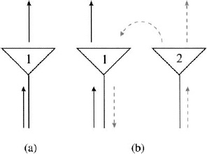
Figure 6.1. Reflected and radiated fields of an array element, (a) An antenna matched to its transmission line radiates with no reflections, (b) A second antenna radiates fields that are received by the first antenna.
If the excitation on element 2 changes, then the apparent reflected signal in element 1 changes. As a result, the element 1 impedance calculated by (6.1) changes. Thus, changing the array excitation, such as beam steering, causes the active element impedance of all the elements to change. The transmitter/receiver that is matched to an isolated element is no longer matched to an element in the array. Even if the impedance of the transmitter/receiver changes to match the element at one excitation, then the transmitter/receiver would no longer be matched if the excitation changes. In order to receive the most power from an incident wave, the element impedance should minimize the total scattering from the array, because less scattering means more of the signal was received by the array.
When antennas are placed close together, as in an array, if one antenna transmits, then all of the others receive some of the signal depending upon the distance and orientation of the antennas [2]. Even when no element is transmitting, an incident wave causes scattering from the elements which effectively makes each element a transmitter. The current on an element is the vector sum of all the currents induced by the fields from the other elements. These element interactions must be understood before designing the array.
This chapter starts by introducing the concept of mutual impedance and the analytical expressions for coupling between two dipoles. There are two parts to examining the effects of mutual coupling on large arrays [3]. The first looks at elements that are surrounded on all sides by many elements. This element appears to be in an infinite array. The second examines the edge effects on the elements close to the edge of a large array or the elements of a small array. It is possible to find the self impedance of the element, and then find the mutual impedances due to the presence of the neighboring elements. The mutual impedances change as a function of scan angle and, under certain conditions, even result in a total reflection of the signal which produces scan blindness at that angle.
6.1. MUTUAL IMPEDANCE
Self-impedance is the impedance of the isolated antenna. The voltage at the antenna terminal is given by Ohm’s law:
If there is no current source at element 1, then the voltage at element 1 due to the current on element 2 is
Z12 is the mutual impedance between elements 1 and 2. The total voltage at element 1 is the sum of (6.2) and (6.3).
The impedance at element 1 is no longer Z11 when element 2 is present. Instead, the impedance is known as the driving point or active impedance of the element and is given by
The value of the mutual impedance depends upon the distance between the elements, the polarization of the elements, the orientation of the elements, and the element patterns.
Mutual coupling occurs in receive arrays, when a plane wave induces a current on elements 1 and 2. The current induced on element 2 radiates and is received by element 1. Adding more elements causes more interactions. If there are N elements, then there are N self-impedances and N(N − 1) mutual impedances. The mutual impedance between any two elements in the array is found by dividing the open-circuit voltage at one element by the current at the other element.
After calculating all the self- and mutual impedances, they can be placed in the N × N impedance matrix.
or

The impedance matrix contains all the self- and mutual impedances of an N-element array. Array element m couples to element n through the mutual impedance Zmn in row m and column n of the matrix. Reciprocity dictates that Zmn = Znm. The driving point impedance for an element in an N element array follows from (6.5):
Alternatively, the coupling can be formulated with admittances instead of impedances. Multiplying both sides of (6.7) by the admittance matrix (inverse of impedance matrix) produces
with the admittance matrix defined as

The driving point admittance is then defined by
Admittance is preferred over impedance for arrays of slots.
6.2. COUPLING BETWEEN TWO DIPOLES
This section presents the analytical equations for mutual coupling between two dipoles. Although these calculations are only valid for two dipoles, they may be applied to any pair of elements in a linear or planar array with or without a ground plane. The elements of the N × N impedance matrix are found by assuming it is composed of N(N − 1) two-dipole mutual impedances and N two dipole self-impedances.
The 2 × 2 impedance matrix for a two-dipole array has elements given by

The driving point impedance at the first element is given by (6.5), and the one at the second element is given by
The Zd is the impedance seen by the transmission line or waveguide of the feed network. When the antenna element is designed and tested in isolation, then Z22 is the impedance. Once the second element is present, then it becomes a determining factor in the impedance of the first antenna element.
The reciprocity theorem is used to find the values of the impedances in (6.6)
Since the current only flows in the y direction and the dipole is very thin,
The y-polarized near field of a dipole oriented along the y axis is
where
For a lone dipole, the power at the current maximum is
The self-impedance is the voltage at the antenna divided by the current fed to the antenna when the antenna is isolated. Assume that the dipole is very thin and that the current runs only along the y axis. This antenna can only radiate and receive electric fields with a y component. The power at the dipole feed point is the integral of the current and the electric field along the dipole.
where ![]() is the electric field at the surface of the dipole. Substituting (6.16) and (6.17) into (6.19) produces
is the electric field at the surface of the dipole. Substituting (6.16) and (6.17) into (6.19) produces

where

Solving the integral in (6.20) leads to [4]

where γ = 0.5772 is Euler’s constant. For a half-wavelength dipole, Z11 = 73 + j42.5.

Figure 6.2. Dipoles placed side by side.
The mutual impedance between two dipoles is found in a similar manner, except the electric field comes from the second dipole, so the values of r, R1 and R2 are different. Assuming that the two dipoles are of the same length, Ly, then the formulas for the mutual impedances are given by:
- Parallel dipoles A and B in Figure 6.2. (A line connecting the centers of the dipoles is perpendicular to the dipoles.)
where

- Collinear dipoles A and C in Figure 6.2. (Dipoles lie along the same line.)
where

- Offset dipoles A and D in Figure 6.2. (The dipoles are parallel, but a line connecting the centers of the dipoles is not perpendicular to the dipoles.)


where

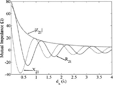
Figure 6.3. Plot of the mutual impedance between two parallel λ/2 dipoles as a function of separation distance in wavelengths.
Figure 6.3 is a graph of the real and imaginary parts of the mutual impedance (Z21 = R21 + jX21) as well as the magnitude of the mutual impedance between two parallel y-oriented dipoles along the x axis. The phase is linear and equal to −kxAB, so it was not included in the plot. The impedance quickly decreases as xAB increases. When xAB = 0, the mutual impedance becomes the self-impedance. Figure 6.4 is a graph of the real and imaginary parts of the mutual impedance as well as the magnitude of the mutual impedance between two collinear y-oriented dipoles along the y axis. The mutual impedance is much smaller than for the parallel dipole case as xAB increases, since the dipole radiation in the y-direction is small. The impedance plots start at yAC = λ/2 instead of yAC = 0, because the dipoles overlap at smaller spacings. Extensive plots of the mutual impedance between two parallel dipoles of different lengths and separation distances in the x and y directions using (6.24) appear in reference 4.
Example. Find the self-, mutual, and driving point impedance of two parallel half-wavelength dipoles (a = 0.001λ) spaced λ/2 apart assuming I1 = I2.
Use (6.5), (6.21), and (6.22) to get Z11 = 73.1309 + j42.5452, Z12 = −12.5324 − j29.9293, and Zd1 = 60.5985 + j12.6159. If I1 ≠ I2, then Zd1 will be different than Zd2, as in an amplitude taper.

Figure 6.4. Plot of the mutual impedance between two collinear λ/2 dipoles as a function of separation distance in wavelengths.
A planar dipole of length L and width w is the complement of a slot of length L and width w. Booker’s relationship introduced in Chapter 4 can also be applied here. Assuming there are two slots in an infinite ground plane, then the mutual admittance between the slots is related to the mutual impedance between two dipoles that are complementary to the slots by [5]
If the slot only radiates from one side of the ground plane, then the relationship is [5]
A slot of width, w, is also considered complementary to a dipole of radius a when the width and radius are related by [5]
Example. Find the self- and mutual admittances of two parallel half-wavelength slots that are complementary to a dipole with a = 0.001λ and are spaced λ/2 apart assuming I1 = I2.
If w ≈ 0.004λ then the slot is complementary to the dipole. Substituting the dipole impedances in the previous examples into (6.25) results in
![]()
Note that the slot is assumed to radiate out both sides.
6.3. METHOD OF MOMENTS
Finding the mutual coupling between nondipole antennas requires numerical methods like the method of moments (MoM). The MoM most closely follows the analytical derivations presented thus far. It is a mathematical technique for solving electromagnetics equations of the form [6]
where ![]() is a linear integrodifferential operator,
is a linear integrodifferential operator, ![]() is the induced current, and
is the induced current, and ![]() is the forcing function. In this equation,
is the forcing function. In this equation, ![]() is known, and the idea is to invert
is known, and the idea is to invert ![]() to obtain the unknown function
to obtain the unknown function
The procedure involves a technique that transforms (6.29) into a system of linear algebraic equations of the form
where ZMM is the MoM impedance matrix, I is the current column vector, and V is the induced voltage column vector. The steps in the MoM procedure are as follows:
- Expand I in into a series of basis functions with unknown coefficients.
- Take the inner product of both sides with a set of known testing functions.
- Apply the boundary conditions at N points to get a set of N equations and unknowns.
- Analytically or numerically solve the definite integral(s) to find ZMM.
- Numerically solve the resultant matrix equation for I.
Once I is known, then the far-field, near-field, efficiency, polarization, or antenna impedance can be easily calculated. The MoM is a powerful technique but works best for
- Electrically small objects
- A perfect electrical conductor (PEC)
- Narrowband applications.
The MoM is widely used to calculate the impedance and radiated fields of many types of antennas.
A thin dipole antenna of radius a has current flowing along its length but not in any other direction. If the wire antenna is situated along the z axis, then [7]
This equation may be rewritten as
Since the wire is a PEC, the current lies only on the surface. If the wire has a radius a, then the volume integral in (6.32) reduces to a surface integral given by
If ![]() (implying that the observation point is on the surface of the wire) and the wire is very thin (a << λ), the resulting current is
(implying that the observation point is on the surface of the wire) and the wire is very thin (a << λ), the resulting current is
and the surface integral of Jz(z′) becomes a line integral of Iz(z′).
If a z-directed field is incident upon the wire, then the total tangential field at the wire surface must be zero or
Substituting (6.35) for the scattered field into (6.36) yields an integral equation of the first kind.

Taking the derivative of inside the integral kernel, K(z, z′), results in
This equation is based on the following approximations:
- The wire is infinitely thin, so that only z-directed currents, not radial or circumfiential currents, exist.
- The wire is a PEC.
- The boundary condition is enforced at the wire surface, but the current, Iz(z′), is a filament at the center of the wire.
- The distance, R, is never zero.
The current on the wire, I(z′) can be written as a sum of weighted basis functions
Next, inserting (6.39) into (6.37) yields [1]
The basis functions, Bn, are mathematical building blocks weighted by the coefficients, In. Equation (6.39) provides an interpolation of the current over the length of the wire. It is possible to solve this integral using Gaussian quadrature if the basis functions are chosen properly. Many different basis functions are used in practice. Subdomain basis functions exist over segmented portions of the wire, while entire domain basis functions exist over the length of wire. Three common examples of subdomain basis functions are [8]:

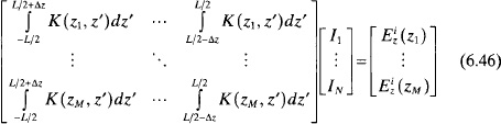
Enforcing the boundary conditions at M points enables (6.40) can be written in matrix form as

The integrals in (6.41) must be solved before finding the coefficients of the basis functions. One way of simplifying the process is to take the inner product of each integral with a weighting function, so that a matrix row is represented by
One common approach is to have the basis and testing functions the same. This technique is known as Galerkin’s method [6]:
If the weighting functions are delta functions, then (6.42) becomes
which reduces to
This formulation is known as point matching [6] or collocation. If point matching is used with pulse basis functions, then applying the boundary conditions at N collocation points yields the matrix equation
As long as Δz is small, then the integral is accurately approximated by midpoint integration.
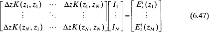
Figure 6.5 shows a diagram of part of the dipole. The wire is broken into segments of length Δz = L/Nseg. The points zm are located at the midpoints on the surface of the wire, while the integration variable z′ is along the filament at the center of the wire.
The next step after calculating the impedance matrix is to represent the right-hand side by either a plane wave (receive antenna) or a voltage source (transmit antenna). A normalized plane wave incident at each segment is [8]
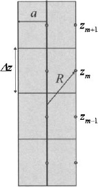
Figure 6.5. Dipole broken into equal segments.
The simplest voltage source is the delta-gap model that has the center segment set to V0.

Example. Find the input impedance to a dipole with L = 0.1λ; and a = 0.005Aλ.
Solution: To easily display the results, only 7 segments are used for the wire. Point matching with pulse basis functions will be used to generate the impedance matrix. The MoM impedance matrix has values given by

The delta gap model is used for the source with V0 = 1/Δz = 70V, so the right-hand side is a 7 × 1 matrix given by
V = [0 0 0 70 0 0 0]T
Solving for the current on the wire segments results in
The small real part and large imaginary part is indicative of a short dipole.
Example. Find the directivity and input impedance for a dipole that is 0.49λ long with a = 0.000001λ.
Solution: Figure 6.6 is a plot of dipole impedance as a function of the number of segments. The real part of the impedance shows little change as a function of the number of segments, while the imaginary part shows dramatic change. Segmentation is not as critical for calculating the directivity (Figure 6.7). The difference between the antenna pattern for the dipole broken into 5 segments and the one broken into 101 segments is barely noticeable in the plot in Figure 6.8. The moral is that a relatively higher segmentation rate is required for accurately calculating the dipole impedance than is required for calculating the antenna pattern.
The MoM also applies to surfaces and dielectrics [7]. For instance, a rectangular patch antenna is divided into small triangles, and the current is found on each of the triangles. Three-dimensional basis functions are used for the triangular grid. Figure 6.9 shows the patch with six different grid levels as listed in Table 6.1. The patch has dimensions of 37.8mm × 50.2mm with a pin feed that is 9.3 mm off center. The substrate has εr = 3.6 with dimensions 53.8mm × 66.2mm × 1.6mm. Using coarse gridding, maximum triangle size of λ/3, produces terrible results for both directivity and impedance calculations as shown in Figures 6.10 and Figure 6.11. Directivity calculations for a grid as coarse as λ/7 are accurate, while λ/5 are very good. As the grid gets finer for impedance calculations, the resonant frequency increases until it hits 2 GHz at λ/11. Increasing to λ/15 improves the depth of S11 at 2 GHz. As the number of triangles increases, the amount of time needed to find the solution increases, and the amount of memory needed also increases. The last column in Table 6.1 is the relative time needed to calculate the antenna pattern of the patch. When the maximum triangle size is λ/15, then the calculations take 506 times longer than when the maximum triangle size is λ/3.

Figure 6.6. Dipole input impedance as a function of segmentation.

Figure 6.7. Dipole directivity as a function of segmentation.

Figure 6.8. Dipole directivity versus angle for 5 and 101 segments.
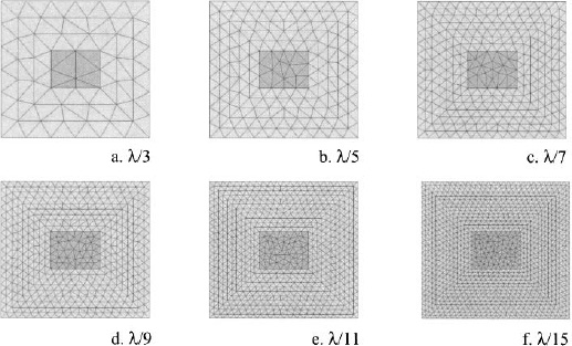
Figure 6.9. Rectangular patch antenna divided into small triangles. The number of unknowns quickly increases as the size of the triangles gets smaller.
TABLE 6.1. Number of Metal and Dielectric Triangles in the Patch Model for a Specified Maximum Triangle Edge Length


Figure 6.10. Patch directivity as a function of triangle size.
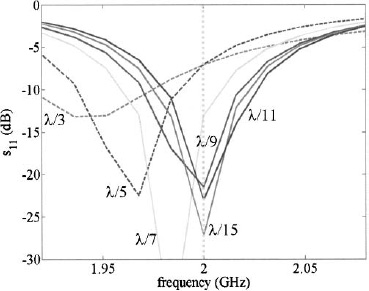
Figure 6.11. Patch S11 as a function of triangle size.
6.4. MUTUAL COUPLING IN FINITE ARRAYS
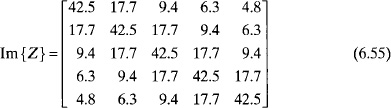
Equations (6.22), (6.23), and (6.24) apply to the mutual impedance between any two elements in an N element array with and without a ground plane. Consider the planar array in Figure 6.12. The diagonal elements of the impedance matrix are all equal to the self-impedance of a dipole and are found using (6.21). Depending upon their locations, the mutual impedance between element m and element n are found using (6.22), (6.23), or (6.24) with

Figure 6.12. Planar array of dipoles on a rectangular grid.
Example. Find the impedance matrix and driving point impedances for 5 parallel λ/2 dipoles spaced λ/2 apart.
The diagonal elements of the impedance are all equal and found using (6.21). The mutual impedance between element m and element n are found using (6.22).


The driving point impedances for the elements when uniformly weighted are given by (6.9):
Example. Find the impedance matrix and driving point impedances for 5 parallel λ/2 dipoles spaced λ apart.
The procedure is repeated for the increased element spacing. Note that the self-impedance does not change, but the mutual impedances are less than those for the same array with λ/2 spacing.

The driving point impedances for this array are given by
More often than not, the dipoles are placed above a ground plane [9]. If the dipole array is above an infinite perfectly conducting ground plane, then the array/ground plane is replaced with the array and an image array at z = −h (Figure 6.13). The currents in the image array are in the opposite direction of the currents in the actual array due to the boundary condition for the tangential electric field. Two impedance matrixes are calculated. The first contains the mutual impedances between all the elements as though there were no ground plane. The second, Zi, contains the mutual impedances between each element and the N images. If the array is z = h above the ground plane, then the image impedance matrix, Zi, is found by solving (6.22), (6.23), or (6.24) using
with yAB and yAD given by (6.50). Once the self- and mutual impedances are found, then the driving point impedance is given by
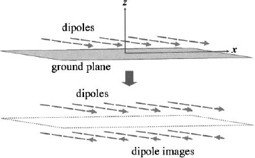
Figure 6.13. Planar array of dipoles on a rectangular grid placed above an infinite ground plane. The ground plane is replaced with an image of the dipoles h below the ground plane with currents opposite those of the array.
The image impedance elements have a negative sign, because the image current flows in the opposite direction of the element currents.
Example. Find the impedance matrix and driving point impedances for 5 parallel λ/2 dipoles spaced λ/2 apart and placed h = λ/4 above an infinite perfectly conducting ground plane.
The ground plane has a dramatic effect on the mutual and self-impedances in the impedance matrix.
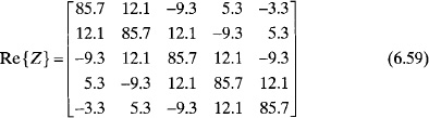

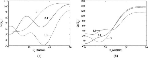
Figure 6.14. Plot of the driving point impedance as a function of scan angle for a 5-element array of parallel λ/2 dipoles spaced λ/2 apart, (a) Real part. (b) Imaginary part.
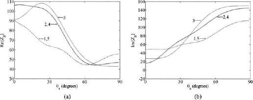
Figure 6.15. Plot of the driving point impedance as a function of scan angle for a 5-element array of parallel λ/2 dipoles spaced λ/2 apart and λ/4 above an infinite perfectly conducting ground plane, (a) Real part, (b) Imaginary part.
Steering the beam changes the mutual impedances between elements. For instance, steering the beam of an N element uniformly spaced linear array changes (6.9) to
Figure 6.14 shows plots of the real and imaginary parts of the driving point impedance as a function of scan angle for a 5-element uniform array of λ/2 parallel dipoles with xAB = 0.5λ. Small scan angles produce small changes in the impedance, while large scan angles produce large changes in the impedance. Figure 6.15 shows the driving point impedances when the array is placed above a ground plane. The ground plane causes a significant change in the scan impedance compared to the case with no ground plane. In both the array with and without a ground plane, the scan impedances begin to significantly change from the impedance at θs = 0 when θs > 30°.

Figure 6.16. Element patterns of an isolated dipole compared to the first 4-element patterns in a 7-collinear-element array.
The mutual coupling in a small finite array affects the radiation of each element differently. For example, a 7-element linear array of uniformly weighted 0.47 λ collinear dipoles spaced half a wavelength apart have element patterns that differ from the isolated element pattern as shown in Figure 6.16. All patterns experience a loss in directivity along with an increase in beam-width. If all 7-element patterns are averaged, then the element pattern in Figure 6.17 results. This average element pattern is symmetric and has a directivity that is 1.5 dB less than the isolated pattern (Figure 6.17). The decrease in directivity corresponds to the increase in beamwidth from 78° to 126°. The fairly fiat-top average element pattern helps keep the main beam constant over a wide scanning angle before the element pattern drops off. Some element patterns squint, while others have many oscillations. If all the element patterns are replaced by the average element pattern, then the array pattern is reasonably reproduced.
Changing the dipole orientation in the array to parallel produces dramatically different element patterns as shown in Figure 6.18. The isolated element pattern is omnidirectional in the plane of the array. The directivity of all the elements actually increases in this case while the beamwidth decreases. As a result, scanning the beam causes the main beam to decrease more than expected. The average element pattern shown in Figure 6.19 is an average of all 7 dipoles in the array. It has a beamwidth of 120°. The average element pattern has a higher gain than the isolated element pattern within ±39° of broadside and has a lower gain farther from broadside.

Figure 6.17. Average versus isolated element patterns in a 7-collinear-element array.
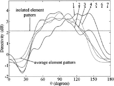
Figure 6.18. Element patterns of an isolated dipole compared to the first 4-element patterns in a 7-parallel-element array.
Mutual coupling not only changes the element patterns, but also changes the input impedance to each of the elements. Figure 6.20 shows the real and imaginary parts of the dipole input impedance for the first four elements in the parallel and collinear arrays when θs = 0°. Element 1 is an edge element and has the most deviation from average. The element orientation does produce different element impedances.

Figure 6.19. Average versus isolated element patterns in a 7-element parallel-element array.

Figure 6.20. Real and imaginary input impedance of the first 4-element patterns in a 7-element array.
Figures 6.21 and 6.22 show the real and imaginary impedances of the center element of an array with N = l, 3, 5, …, 25 elements. The single element array has the expected impedance of an isolated dipole. Adding one dipole to either side produces over a 10% change in the impedance of the center dipole. The input impedance of the parallel dipoles is more susceptible to mutual coupling than the collinear dipoles. After a while, adding more elements does not change the impedance. Consequently, a dipole surrounded by a large number of elements will have the same impedance as a dipole in an infinite array.

Figure 6.21. Real part of the center element impedance as a function of the number of element on either side of it.

Figure 6.22. Imaginary part of the center element impedance as a function of the number of element on either side of it.
The center element pattern also changes as the number of elements in the array grows. Figure 6.23 shows the element pattern of the center element of a parallel array of dipoles spaced 0.5λ apart with N = 1, 3, 5, …, 25. The number of ripples in the element pattern increases with N. Changes to the center element pattern decrease as N increases, because each additional element is farther away than the center element.

Figure 6.23. Center element pattern in an array of N = 1, 3, 5, …, 25 parallel elements with d = 0.5λ.

Figure 6.24. Center element pattern in an array of 1, 3, 5, and 7 collinear elements d = 0.5λ.
Element spacing plays a major role in the effect on the element patterns. When a collinear array of dipoles are spaced 0.5λ apart, then the center element pattern dramatically changes with the addition of elements as shown in Figure 6.24. Increasing the spacing to 0.75λ causes little change to the center element pattern (Figure 6.25).

Figure 6.25. Center element pattern in an array of 1, 3, 5, and 7 collinear elements d = 0.75λ.
6.5. INFINITE ARRAYS
Elements in the center of a large array behave as though the array were infinite in extent. As shown previously, as more elements surround a center element, the impedance and pattern of the center element changes less. Calculating the impedance of an element in an infinite array is much easier than calculating the same impedance for an element in a finite array. The advantage of doing the calculations with an infinite array is that calculations are done on a single element with periodic boundary conditions applied.
An infinite array has the following characteristics:
- All elements are placed in a periodic lattice.
- All elements are identical.
- It has uniform amplitude weights.
- Relative phase between two adjacent elements is a constant.
- It radiates a plane wave.
- It has infinite directivity.
- It has no sidelobes.
The infinite array derives its characteristics from a uniform array when N → ∞. In the limit, the array factor becomes a Dirac delta function.
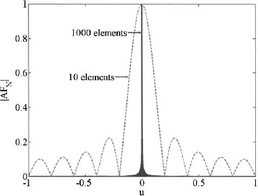
Figure 6.26. Normalized array factors for 10- and 1000-element uniform arrays.
Figure 6.26 is a visual demonstration of (6.63) as N increases from 10 to 1000 when d = 0.5λ and the array factors are normalized. The 1000-element array factor looks very similar to a delta function. The main beam and grating lobes appear at locations given by the equations in Chapter 2. Since an infinite array transmits an infinite amount of power at one angle, the directivity is infinite.
All the elements in an infinite array see the same environment, so they all have the same reflection coefficient. Since the reflection coefficient, Γ, is a function of scan angle, then the realized gain for a lossless element is related to the gain of the element by [2]
It is important that Γ stays small within the scan range of the array. Thus, finding Γ or the element impedance is very important in array design.
6.5.1. Infinite Arrays of Point Sources
Consider the case of an infinite linear array of point sources spaced d along the x axis. If the elements have equal amplitude weights and a beam steering phase shift, then the current at element n is given by
when the beam is steered to θs and kxs = k sin θs. The array factor is given by

Using the sifting property of the delta function, the array factor is written as
This equation looks like the array factor for a uniform array, except there are an infinite number of elements.
If a periodic function has slowly decaying terms, then it Fourier transform has terms that quickly decay. The Poisson sum relates an infinite periodic series to its infinite periodic Fourier transform and is given by
where ![]() is the Fourier transform of f. Since k = 2π/λ and the 2π is already contained in the variable, the following formulation for Fourier transforms is used:
is the Fourier transform of f. Since k = 2π/λ and the 2π is already contained in the variable, the following formulation for Fourier transforms is used:
The infinite Fourier series in (6.67) can be replaced by an infinite sum of Dirac delta functions using the Poisson sum formula.
This expression for the array factor is called the grating lobe or Floquet series [2], because the location of the Dirac delta functions (Floquet modes) are the same as the location of the grating lobes (see Chapter 2).
A similar derivation is possible for planar arrays. If the planar array in the x−y plane has rectangular spacing, then

Using the Poisson sum, (6.72) becomes [10]

The grating lobe series for point sources in an infinite array with triangular spacing is given by
An interesting observation from these grating lobe series is that the antenna radiates a plane wave at very specific angles and nowhere else. In other words, there are no sidelobes. The grating lobe series is frequently referred to as a Floquet series. Each main lobe that radiates is known as a Floquet mode. Thus, the total power radiated is the sum of all the Floquet modes, because there are no sidelobes.
Example. Graph and label the Floquet modes for a 1000-element uniform array with d = 1.0λ steered 30° from broadside. Figure 6.27 shows the plots. Since the 1000-element array factor looks like two delta functions, they can be treated as two Floquet modes.
6.5.2. Infinite Arrays of Dipoles and Slots
The driving point impedance of a Lx × wy flat dipole or slot in an infinite array in a dx × dy rectangular lattice (Figure 6.28) can be calculated analytically using the following formulas [11]:
- Dipoles in free space:
Figure 6.27. Normalized array factors for 10- and 1000-element uniform arrays with d = 1.0λ and steered 30° from broadside.
- Dipoles h above a ground plane:
- Slots in a a × b rectangular waveguide:


where
![]()

Figure 6.28. Infinite rectangular lattice of flat dipoles or slots.
These formulas are not sensitive to wy.
Example. Plot the normalized driving point resistance for a half wavelength dipole in an infinite array with dx = 0.5λ and dy = 0.5λ in free space and 0.25λ above a ground plane.
Figure 6.29 is a plot of the real part of (6.75), and Figure 6.30 is a plot of the real part of (6.76). The array is scanned as a function of θ in the E plane (![]() = 0°), the diagonal plane (
= 0°), the diagonal plane (![]() = 45°), and the H plane (
= 45°), and the H plane (![]() = 90°). The plots are nearly identical until about 20° when they begin to diverge. There is a 50% spread in the normalized resistance at 35° for the no ground plan case and at 37° for the ground plane case.
= 90°). The plots are nearly identical until about 20° when they begin to diverge. There is a 50% spread in the normalized resistance at 35° for the no ground plan case and at 37° for the ground plane case.

Figure 6.29. Real part of the driving point impedance of an infinite array of half-wavelength dipoles.

Figure 6.30. Real part of the driving point impedance of an infinite array of half-wavelength dipoles 0.25λ above a ground plane.
Another approach to the analysis of infinite arrays is to place an element inside a unit cell. As an example, Figure 6.31 shows a unit cell that contains a slot in an infinite array [3]. The unit cell extends from the array to infinity in the z direction. The walls of the unit cell have either electric or magnetic boundary conditions, depending upon the direction of the electric or magnetic fields in the slots. The walls do not perturb the fields; but once the walls are in place, all fields outside the walls can be ignored. In a way, the unit cell behaves like a waveguide. As shown in Figure 6.31, the magnetic walls are parallel to the electric field in the slot while the electric walls are parallel to the magnetic field in the slot.

Figure 6.31. Unit cell bounding a slot element in an infinite array.
The dominant mode in the unit cell waveguide is TEM. Only one mode exists if the size of the waveguide (element spacing) is chosen properly for the operating frequency. If there are no higher-order modes, then there are no grating lobes either. When the array scans in the x−z plane, the amplitude of the fields remains the same, but a constant phase difference exists between consecutive slots. Opposite walls of the unit cell are identical except for a phase difference that is a function of the steering angle. In the unit cell, the walls parallel to the long slot dimension remain electric walls while the other walls differ by a phase shift. The dominant mode in the unit cell becomes TE since a longitudinal component of the field is present in the z direction. Scanning in the y−z plane produces a dominant TM mode. Scanning at arbitrary angles produces both TE and TM modes.
Assume the elements in the infinite array lie in a plane with
where γ = 90° is rectangular spacing. All the Floquet modes associated with this element spacing have propagation constants given by
The dominant Floquet mode or main beam occurs when m and n are zero.
Floquet modes become propagating modes or grating lobes when kzmn ≥ 0 or
Example. If a planar array is scanning in the x−z plane, find the maximum element spacing that still excludes the m = 0 and n = 0 Floquet mode.
The dominant mode occurs when m = 0 and n = 0. The first higher-order mode occurs when m = 1 and n = 0 leading to kz = |k sin θ − 2π/dx|. To keep this mode below cutoff, then k < kz and
which is the same as the element spacing where no grating lobes appear.
6.6. LARGE ARRAYS
Some tricks can be played to reduce the computation time for calculating the characteristics of a large array. As the array gets larger, more elements have neighboring elements completely surrounding them, so the mutual coupling of these elements is similar. As such, they can be treated to have identical characteristics with small variations that tend to average out as the number of elements increases. The percent of edge elements in a rectangular planar array with a rectangular element grid is given by
A contour plot of (6.86) appears in Figure 6.32. The number of edge elements depends upon the total number of elements in the array and the ratio of Nx to Ny. As an example, a 400-element rectangular planar array with a rectangular element grid has 24% edge elements when it is 40 × 10, and it has only 19% edge elements when it is 20 × 20. A square array always has fewer edge elements than a rectangular array. If the array increases in size until it is 40 × 40, then the percent of edge elements decreases to 9.75%. Other array contours, such as a hexagonal shape, have even more edge elements than predicted by (6.86).
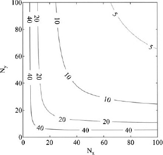
Figure 6.32. Percentage of edge elements in a rectangular planar array with a rectangular element grid.
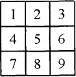
Figure 6.33. A 3 × 3 array with 8 edge elements and 1 center element.
A 3 × 3 square array on a square lattice (Figure 6.33) has 9 elements with 9 different element patterns. If the elements are dipoles, then the patterns can be calculated using the MoM as shown in Figure 6.34. Elements 1, 3, 7, and 9 have the same pattern but are rotated by 0°, 90°, 180°, and 270°, respectively. Element pattern 4 is flipped 180° relative to element 6. Element pattern 2 is flipped 180° relative to element 8. Element 5 is in the center and has a unique pattern that is symmetric about x and y.
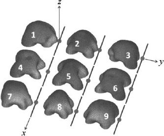
Figure 6.34. Element patterns of a 3 × 3 array of dipoles.
Calculating the array far-field pattern and mutual coupling when a large array has more complicated elements than dipoles requires a lot of computer time and memory. The first approach to reducing computer time and memory requirements is to use numerical methods suited to the problem at hand, such as the fast multiple method (FMM). The second approach is to find a representative element pattern that includes mutual coupling effects. Multiplying this pattern times the array factor yields an accurate approximation of the array far-field pattern.
6.6.1. Fast Multipole Method
The FMM was named one of the “Top Ten Algorithms of the Century” [12] and has found extensive use in electromagnetics. FMM accelerates the iterative solver in the MoM by replacing the Green's function using a multipole expansion that groups sources lying close together and treats them like a single source [13]. Figure 6.35 shows that the sources lying in region Q that independently interact with P can be grouped together and replaced by a single source that interacts with P. Both MoM and FMM use basis functions to model interactions between triangles and segments, but unlike MoM, FMM groups basis functions and computes the interaction between groups of basis functions, rather than between individual basis functions. Figure 6.36 is a diagram of the hierarchical spatial decomposition that separates the simulation space into regions that are far enough apart to interact according to the approximate grouping shown in Figure 6.35. As the distance increases, larger regions of space can be grouped into single approximations. By treating the interactions between far-away basis functions using the FMM, the corresponding matrix elements do not need to be explicitly stored, resulting in a significant memory requirement [13]. The FMM can reduce the matrix–vector product in an iterative solver from O(N2) to O(N log N) in memory [14].
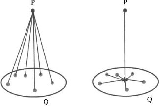
Figure 6.35. Fast multipole method.

Figure 6.36. Diagram of the spatial decomposition used in FMM.
The FMM often creates incredible memory and time savings when applied to antennas, such as an array of dipole antennas. Consider a square array of N dipoles in a square grid with element spacing d = λ/2. As shown in Figure 6.37, the amount of memory required for FMM increases linearly with the number of elements, and Figure 6.38 shows a similar graph for time. Memory and time requirements for the MoM increase extremely fast. In fact, for a 21 × 21 array, the MoM takes 1700 MB and 2977s, while the FMM only takes 75.5 MB (22.5 times less) and 79s (37.7 times less). In this case, the FMM models a much larger array than does the MM alone.
The FMM is not always superior to the MoM, though. If the elements in an array are spaced far apart, then the calculations using FMM are very slow compared to MoM. Calculating the currents and far field of a 5 × 20 array of dipoles spaced λ/2 apart is done much more efficiently using FMM. In that case, the calculation only requires 24s versus 314s using MoM, which is 13 times faster. On the other hand, increasing the element spacing to 10λ increases the FMM calculation to 5719s while not changing the MoM calculation time. This means the FMM was 18 times slower. Thus, FMM becomes slow when the sources are spread far apart in space.

Figure 6.37. Maximum memory used to calculate the currents on an array of N dipoles.
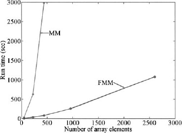
Figure 6.38. Time used to calculate the currents on an array of N dipoles.
As another example, the patch antenna meshed in Table 6.1 is modeled using FMM and MM. Table 6.2 shows the time and memory requirements for this problem using MM and FMM when the maximum triangle length is λ/5 and λ/15. In this case, the FMM takes more memory and more time than the MoM. Although FMM can offer exceptional speed and memory use improvements in many problems, there are situations where FMM does not work well, and the user should beware.
TABLE 6.2. Time and Memory Needed to Calculate the S11 of a Patch Antenna Using Both MoM and Fast Multipole Method


Figure 6.39. Array pattern found by using the average element pattern compared with the FMM solution at ![]() = 0.
= 0.
6.6.2. Average Element Patterns
An average element pattern is the average of all the element patterns in the array. Replacing all the element patterns with the average element pattern and then multiplying by the array factor results in an accurate reproduction of the array pattern. The element pattern for each element in the array is calculated when all other elements are terminated in a matched load. Their average then replaces each element in the array. Since the pattern contains mutual coupling effects, the resulting array pattern is more accurate than when an isolated element pattern is used. As an example, consider a planar array of x-oriented half-wavelength dipoles spaced λ/2 apart with 20 elements in the y direction and 5 elements in the x direction. A 25-dB Taylor taper is placed across the y direction while a uniform taper is in the x direction. Figure 6.39 is a cut of the array pattern at ![]() = 0, while Figure 6.40 is a cut of the array pattern at
= 0, while Figure 6.40 is a cut of the array pattern at ![]() = 90°. The FMM solution and the average element pattern solution agree well for the
= 90°. The FMM solution and the average element pattern solution agree well for the ![]() = 90° cut, but not so well for the
= 90° cut, but not so well for the ![]() = 0° cut. Even though the
= 0° cut. Even though the ![]() = 90° cut is low sidelobe, it has more elements and a lower percentage of edge elements, so the averaging works better.
= 90° cut is low sidelobe, it has more elements and a lower percentage of edge elements, so the averaging works better.

Figure 6.40. Array pattern found by using the average element pattern compared with the FMM solution at ![]() = 90°.
= 90°.
6.6.3. Representative Element Patterns
Another approach is to calculate the element patterns for each element in a 3 × 3 array as shown in Figure 6.33. There are 9 different element patterns, only 4 if rotations are not included. These element patterns replace similar element patterns in larger arrays that have the same element grid as the 3 × 3 array. Thus, for Nx × Ny array, the element patterns of elements 1, 3, 7, and 9 of the 3 × 3 array are placed at the corners of the Nx × Ny array. Elements 2, 4, 6, and 8 replace the elements on the edges of the larger array. Finally, element 5 of the 3 × 3 array replaces all interior elements of the Nx × Ny array. Table 6.3 lists the number of element patterns from the 3 × 3 array that are used in an Nx × Ny array. For instance, the element patterns of a 5 × 20 element array of dipoles spaced dx = dy = 0.5λ in a square grid can be represented by the elements in the 3 × 3 as shown in Figure 6.41. Using this approach results in the array patterns shown in Figures 6.42 and 6.43. At least for this array, the average element pattern worked better than the representative element pattern approach. The results deviate at the peak of the main beam as well as in the sidelobes. Even though the average element pattern results are better, calculating the average element pattern of a large array takes considerable more time than calculating the 9-element patterns of a 3 × 3 array (only 4-element patterns are needed if symmetry is invoked).
TABLE 6.3. Number of Elements from the 3 × 3 Used in a Nx × Ny Array


Figure 6.41. A 5 × 20 array is built from the 9 element patterns.

Figure 6.42. Array pattern (![]() = 0°) for a 5 × 20 array found by using the element patterns from the 3 × 3 array.
= 0°) for a 5 × 20 array found by using the element patterns from the 3 × 3 array.
6.6.4. Center Element Patterns
Figure 6.44 shows the element patterns for each element in a 3-element array of parallel dipoles lying in the x direction, spaced λ/2 apart along the y axis. Averaging these element patterns produces the lower-gain, symmetric pattern labeled “3 avg”. Calculating the array pattern by multiplying this element pattern times the array factor is much faster than calculating the array pattern using a full wave electromagnetic solver for the large array. The question is whether such an approach yields accurate results.

Figure 6.43. Array pattern (![]() = 90°) for a 5 × 20 array found by using the element patterns from the 3 × 3 array.
= 90°) for a 5 × 20 array found by using the element patterns from the 3 × 3 array.

Figure 6.44. Element patterns from a 3-element array of parallel dipoles lying in the x direction, spaced λ/2 apart along the y axis with their average element pattern.
Figure 6.44. The element patterns from a 3-element array of parallel dipoles lying in the x direction, spaced λ/2 apart along the y axis with their average element pattern.
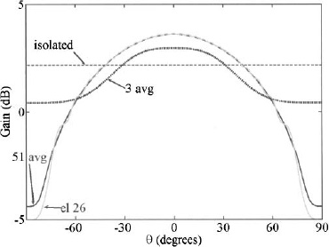
Figure 6.45. Element patterns associated with the 51-element array.
Consider a 51-element array of parallel dipoles lying in the x direction, spaced λ/2 apart along the y axis. The average element pattern for this array along with the center element pattern (element 26) are graphed in Figure 6.45 along with the isolated element pattern and the “3 avg” pattern from Figure 6.44. The average element pattern and the element pattern of element 26 are nearly identical and would be very close to the element pattern in an infinite array. Multiplying the element patterns in Figure 6.45 by the array factor for a 51-element array results in the antenna patterns shown in Figure 6.46. The FMM solution for the full array is also shown for comparison. The biggest discrepancy between these patterns occurs at the main beam and the far-out sidelobes. The expanded areas in Figure 6.46 show that the center element and the average element pattern for the 51-element array provide excellent matches to the FMM solution. Since calculating 51-element patterns, averaging them, and then multiplying by the array factor takes longer than the FMM solution, the best approach is to use the element pattern of the center element of the large array to represent all element patterns in the array. Calculating the element pattern for an infinite array or the center element pattern is easier and faster than calculating the element pattern of the center element of a large array, so it is the preferred approach.
Example. Compare the center and average element patterns of a 3 × 3 array of rectangular patches to the element pattern of the patch in an infinite array (Figures 6.47–6.50).
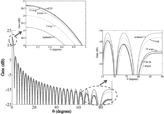
Figure 6.46. Array pattern for the 51-element array calculated using FMM and four approaches to multiplying an element pattern times the array factor.

Figure 6.47. A 3 × 3 array of rectangular patches.
6.7. ARRAY BLINDNESS AND SCANNING
Arrays must be designed for their entire scanning range, not just for broadside. Wheeler showed that for any infinite array, the impedance at a scan angle, θs, is approximately equal to [15]

Figure 6.48. Element patterns of the 3 × 3 array of rectangular patches.

Figure 6.49. Element pattern cuts (![]() = 0°) for the average, infinite array, and center element patterns.
= 0°) for the average, infinite array, and center element patterns.
In an E-plane scan, the impedance approaches infinity toward endfire, while for the H-plane scan, the impedance approaches zero at endfire. This result is independent of element spacing. The emergence of grating lobes, which is a function of element spacing, also causes extreme impedance mismatch. As a result, element spacing must be small at the highest frequency and maximum scan angle to preclude the emergence of a grating lobe.

Figure 6.50. Element pattern cuts (![]() = 90°) for the average, infinite array, and center element patterns.
= 90°) for the average, infinite array, and center element patterns.
Lechtreck discovered another scan limiting phenomenon that causes a large impedance mismatch closer to broadside than the angle where grating lobes emerged [16]. The mismatch caused a large dip in the E-plane element pattern due to a surface wave on the face of the array. He postulated that this blindness angle occurs when
where d is the element spacing in the scan plane, vs is phase or slow wave velocity of a surface wave traveling along the array, c0 is the velocity of light in free space, and λ0 is the wavelength in free space. Note that this equation reduces to the equation for predicting grating lobes when vs = c0, or all the radiation travels away from the array. Lechtreck verified (6.88) by measuring a significant dip in the center element pattern at ±67° of a rectangular 65-element array with hexagonal spacing when d = 0.506λ and vs 0.93c0 (measured). Decreasing the surface wave velocity causes the blindness to occur closer to broadside. Decreasing the element spacing moves the blindness angle away from broadside [17].
Scan blindness occurs when an array neither transmits nor receives power (100%—or at least a very large amount—is reflected) at certain scan angles. It occurs when the steering phase of the elements matches the phase propagation of a surface wave on the face of the antenna. Thus, an electromagnetic wave excited by the elements travels as a surface wave rather than propagating away from the face of the array. In order to induce scan blindness, a structure that can support a slow wave must be near or on the array face [18]. Waveguide arrays with dielectric covers, microstrip arrays over a thick dielectric substrate, and corrugated surfaces are examples where waves become trapped inside the dielectric slab and propagate parallel to the elements. Scan blindness becomes worse as the array size increases and is not a severe problem for small arrays. Complete scan blindness when 100% of the power is reflected from the elements only occurs in infinite arrays [19].
Scanning to the blind angle means that kz becomes imaginary while a surface wave mode propagates along the surface of the array. Blindness occurs when the imaginary part of the impedance becomes extremely large even when the real part may be nonzero [20]. In order for blindness to occur, kz must be zero, and the wave propagation constant must equal the surface wave propagation constant.
Surface waves exist in a dielectric substrate of thickness h when for the TE mode when [21]
and for the TM mode when
where 0 in the subscript indicates free space and d indicates dielectric. For substrates with ![]() only the lowest order TM surface wave mode exists. If there are only currents in the x direction (e.g., x-oriented printed dipoles), then polarization mismatch prevents a TM surface wave for H-plane scanning. The surface wave propagation constant should include the presence of the microstrip patches, but for most practical purposes, the patches can be ignored and the unloaded surface wave propagation constant used with an error in blindness angle of much less than one degree [22].
only the lowest order TM surface wave mode exists. If there are only currents in the x direction (e.g., x-oriented printed dipoles), then polarization mismatch prevents a TM surface wave for H-plane scanning. The surface wave propagation constant should include the presence of the microstrip patches, but for most practical purposes, the patches can be ignored and the unloaded surface wave propagation constant used with an error in blindness angle of much less than one degree [22].
Schaubert found that E-plane scan blindness in single polarized arrays of tapered slot antennas with a ground plane can be predicted by approximating a corrugated surface parallel to the x–z plane with corrugations t thick and h tall (length of TSA) and separated by the element spacing, dx. He found that blindness occurs when [23]
If a − t > λ/2, then a TMz mode with the electric field in the y-z plane exists between the parallel plates. The dielectric thickness and permittivity of a TSA do not greatly affect the blindness for the thin dielectric substrates used to make them. The scan blindness is very dependent on the H-plane separation and the length of the depth of the corrugation. Blindness moves toward endfire as the H-plane spacing, frequency, or antenna depth increases.
Example. Plot the blind angle over a frequency range of 3.8 to 4.2 GHz for an infinite planar array of TSAs that scan in the E plane. Assume h = 3.5 cm, dx = dy = 4.43 cm.
Figure 6.51 shows the plot of the blind angle as a function of frequency. Increasing the frequency moves the blind angle away from broadside.
Usually, the dielectric slab is very thin, so only the lowest-order TM mode propagates. The first TM surface wave propagation constant is bounded by ![]() . A surface wave resonance occurs when ksw equals a Floquet mode propagation constant or [10]
. A surface wave resonance occurs when ksw equals a Floquet mode propagation constant or [10]

Figure 6.51. Scan blindness as a function of frequency for the E-plane TSA array.

Figure 6.52. Infinite array of open-ended rectangular waveguides.
When ![]() is small, then
is small, then
Example. An infinite planar array of X-band rectangular waveguides are in a rectangular lattice in the x-y plane (Figure 6.52). Assume a = 2.29 cm, b = 1.02, and the wall thickness is 1mm. Use the unit cell approximation to plot the E-plane and H-plane element patterns at 10 GHz.
Figure 6.53 shows the plot of the E-plane and H-plane element patterns of the array.
6.8. MUTUAL COUPLING REDUCTION/COMPENSATION
Changing the array environment changes the mutual coupling. Adding a ground plane to a dipole array improves the H-plane scan but deteriorates the E-plane scan. In order to improve the E-plane scan without affecting the H-plane scan, a periodic array of conducting baffles is placed between the dipoles.
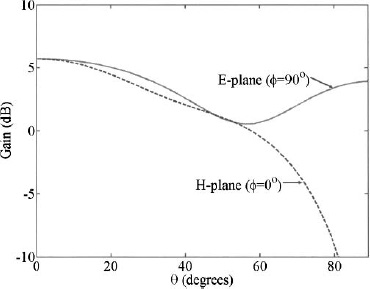
Figure 6.53. E-plane and H-plane element patterns of the infinite array of rectangular waveguides.
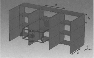
Figure 6.54. Infinite array of open-ended rectangular waveguides with fences in the y-z plane.
If the baffles are thin, perpendicular to the ground plane, and running between the dipoles or slots, the baffles will not change the H-plane scanning behavior. The height of the baffles determines their effect on the E-plane scan [24].
Example. The infinite planar array of X-band rectangular waveguides in Figure 6.52 are modified to have metallic fences in the (a) E plane (Figure 6.54) and (b) H plane (Figure 6.55). Show how the height of the fences changes the element patterns at 10 GHz.

Figure 6.55. Infinite array of open-ended rectangular waveguides with fences in the x–z plane.

Figure 6.56. H-plane element pattern as a function of h.
As can be seen in Figure 6.56, the E-plane fences induce a null in the H-plane element pattern. The null gets deeper and moves away from broadside as the fence gets taller. Figure 6.57 shows that the E-plane element pattern has a higher gain out to about 60° due to the fences. Fences in the x–z plane have no effect on the H-plane element pattern (Figure 6.58) but move the dip in the E-plane pattern away from broadside as well as increase its depth (Figure 6.59). The h = 10 fence induces a very flat element pattern from 0° to 45°. Another dip in the pattern begins to form at 37° for h = 15 mm. It also gets deeper and moves to a higher angle when h = 20 mm.

Figure 6.57. E-plane element pattern as a function of h.

Figure 6.58. H-plane element pattern as a function of h.
The easiest way to reduce the deleterious effects of mutual coupling is to pack the elements closer together, so that grating lobes do not enter real visible space [25]. Unfortunately, moving the elements closer together also implies the use of narrowband elements. Changing the impedance of the ground plane between elements by using corrugations [26] allows larger element spacings before blindness occurs.

Figure 6.59. E-plane element pattern as a function of h.
Mutual coupling in a transmit only array can be dramatically reduced by using a circulator with one port terminated with a matched load [27]. This approach cannot be used as a receive array, because the received signal would also be sent to the matched load as well.
A tunable element has an impedance that is a function of the scan angle of the array. This approach is complex and expensive and limits bandwidth.
The position of the element null is a function of the dielectric substrate height and permittivity. Decreasing the height of the dielectric substrate moves the scan blindness closer to endfire. Decreasing the dielectric constant of the substrate will also move the scan blindness closer to endfire.
Example. Demonstrate the effects of dielectric cover thickness and permittivity on the infinite planar array of X-band rectangular waveguides in Figure 6.52.
Figure 6.60 shows the infinite array with a dielectric cover (εr = 2) h thick. Figures 6.61 and 6.62 are the H- and E-plane element patterns for several different values of h. The dip in the E-plane pattern becomes more prominent as the thickness increases. Figures 6.63 and 6.64 are the H- and E-plane element patterns for several different values of εr when h = 10 mm. The dips in both patterns significantly increase with an increase in εr.
Surface waves in a microstrip patch substrate can be suppressed by the proper choice of thicknesses for given material properties [28]. The dominant TM surface wave associated with a circular patch can be suppressed by properly selecting the patch size. Unfortunately, the optimum size is not resonant.
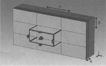
Figure 6.60. Infinite array of open-ended rectangular waveguides with a dielectric cover.
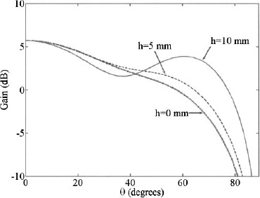
Figure 6.61. H-plane element patterns for different thicknesses of dielectric cover.
Two ways to reduce the circular patch size while eliminating the surface wave are [29]:
- Place a cylindrical core (radius less than the radius of the patch) of dielectric material with a dielectric constant less than the substrate beneath the circular patch.
- Make the patch an angular ring with several equally spaced shorting pins.

Figure 6.62. E-plane element patterns for different thicknesses of dielectric cover.

Figure 6.63. H-plane element patterns for different permittivities of dielectric cover.
More recent approaches to mitigating the effects of mutual coupling use electromagnetic bandgap (EBG) materials to eliminate surface waves in microstrip arrays. As the substrate dielectric constant increases, the bandwidth decreases. The increased thickness encourages the propagation of unwanted surface waves. Placing a mushroom style EBG structure between the patches has been experimentally shown to reduce coupling between adjacent patches by up to 8dB [30]. This approach was extended to eliminate scan blindness in an infinite array of rectangular patches [31]. Several other mutual coupling/scan blindness mitigation techniques using EBG structures have also been proposed [32–35]. Figure 6.65 is a diagram of an array of rectangular microstrip patches in the midst of an EBG structure.

Figure 6.64. E-plane element patterns for different permittivities of dielectric cover.
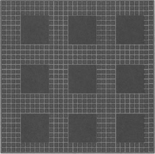
Figure 6.65. Rectangular microstrip patches surrounded by EBG structure.
REFERENCES
- W. L. Stutzman and G. A. Thiele, Antenna Theory and Design, 2nd ed., New York: John Wiley & Sons, 1998.
- J. L. Allen and B. L. Diamond, Mutual Coupling in Array Antennas, Technical Report EDS-66-443, Lincoln Laboratory, 1966.
- S. Edelberg and A. Oliner, Mutual coupling effects in large antenna arrays: Part 1–Slot arrays, IRE Trans. Antennas Propagat., Vol. 8, No. 3, 1960, pp. 286–297.
- H. King, Mutual impedance of unequal length antennas in echelon, IRE Trans. Antennas Propagat., Vol. 5, No. 3, 1957, pp. 306–313.
- R. S. Elliott, Antenna Theory and Design, revised edition, Hoboken, NJ: John Wiley & Sons, 2003.
- R. F. Harrington and IEEE Antennas and Propagation Society, Field Computation by Moment Methods, Piscataway, NJ: IEEE Press, 1993.
- A. F. Peterson, S. L. Ray, and R. Mittra, Computational Methods for Electromagnetics, New York: IEEE Press, 1998.
- C. A. Balanis, Advanced Engineering Electromagnetics, New York: John Wiley & Sons, 1989.
- P. Carter, Jr., Mutual impedance effects in large beam scanning arrays, Antennas Propagation, IRE Trans. Vol. 8, No. 3, 1960, pp. 276–285.
- A. Bhattacharyya, Phased Array Antennas and Subsystems: Floquet Analysis, Synthesis, BFNs, and Active Array Systems, Hoboken, NJ: Wiley-Interscience, 2006.
- A. A. Oliner and R. G. Malech, Mutual coupling in infinite scanning arrays, in Microwave Scanning Antennas, R. C. Hansen, ed., New York: Academic Press, 1966, pp. 195–335.
- J. Dongarra and F. Sullivan, Guest Editors Introduction to the top 10 algorithms, Comput. Sci. Eng., Vol. 2, No. 1, 2000, pp. 22–23.
- J. Board and L. Schulten, The fast multipole algorithm, Comput. Sci. Eng., Vol. 2, No. 1, 2000, pp. 76–79.
- A. T. Ihler, An Overview of Fast Multipole Methods, Cambridge: MIT, 2004.
- H. Wheeler, The grating-lobe series for the impedance variation in a planar phased-array antenna, IEEE Trans. Antennas Propagat., Vol. 14, No. 6, 1966, pp. 707–714.
- L. Lechtreck, Effects of coupling accumulation in antenna arrays, IEEE Trans. Antennas Propagat., Vol. 16, No. 1, 1968, pp. 31–37.
- H. A. Wheeler, A systematic approach to the design of a radiator element for a phased-array antenna, Proc. IEEE, Vol. 56, No. 11, 1968, pp. 1940–1951.
- D. Pozar and D. Schaubert, Scan blindness in infinite phased arrays of printed dipoles, IEEE Trans. Antennas Propagat., Vol. 32, No. 6, 1984, pp. 602–610.
- G H. Knittel, A. Hessel, and A. A. Oliner, Element pattern nulls in phased arrays and their relation to guided waves, Proc. IEEE, Vol. 56, No. 11, 1968, pp. 1822–1836.
- A. K. Bhattacharyya, Floquet-modal-based analysis for mutual coupling between elements in an array environment, IEE Proc. Microwaves Antennas Propagat., Vol. 144, No. 6, 1997, pp. 491–497.
- D. M. Pozar, Analysis and design considerations for printed phased-array antennas, in Handbook of Microstrip Antennas, J. R. James and P. S. Hall, eds., Stevenage, UK: Peregrinus, 1989, 693–754.
- D. Pozar and D. Schaubert, Analysis of an infinite array of rectangular microstrip patches with idealized probe feeds, IEEE Trans. Antennas Propagat., Vol. 32, No. 10, 1984, pp. 1101–1107.
- D. H. Schaubert, A class of E-plane scan blindnesses in single-polarized arrays of tapered-slot antennas with a ground plane, IEEE Trans. Antennas Propagat., Vol. 44, No. 7, 1996, pp. 954–959.
- S. Edelberg and A. Oliner, Mutual coupling effects in large antenna arrays II: Compensation effects, IRE Trans. Antennas Propagat., Vol. 8, No. 4, 1960, pp. 360–367.
- A. W. Rudge, The Handbook of Antenna Design, 2nd ed., London: P. Peregrinus on behalf of the Institution of Electrical Engineers, 1986.
- E. DuFort, Design of corrugated plates for phased array matching, IEEE Trans. Antennas Propagat., Vol. 16, No. 1, 1968, pp. 37–46.
- R. C. Hansen, Microwave Scanning Antennas, New York: Academic Press, 1964.
- N. Alexopoulos and D. Jackson, Fundamental superstrate (cover) effects on printed circuit antennas, IEEE Trans. Antennas Propagat., Vol. 32, No. 8, 1984, pp. 807–816.
- D. R. Jackson, J. T. Williams, A. K. Bhattacharyya et al., Microstrip patch designs that do not excite surface waves, IEEE Trans. Antennas Propagat., Vol. 41, No. 8, 1993, pp. 1026–1037.
- Y. Fan and Y. Rahmat-Samii, Microstrip antennas integrated with electromagnetic band-gap (EBG) structures: A low mutual coupling design for array applications, IEEE Trans. Antennas Propagat., Vol. 51, No. 10, 2003, pp. 2936–2946.
- F. Yunqi and Y Naichang, Elimination of scan blindness in phased array of microstrip patches using electromagnetic bandgap materials, Antennas Wireless Propagat. Lett. IEEE, Vol. 3, 2004, pp. 63–65.
- Z. Iluz, R. Shavit, and R. Bauer, Microstrip antenna phased array with electromagnetic bandgap substrate, IEEE Trans. Antennas Propagat., Vol. 52, No. 6, 2004, pp. 1446–1453.
- G. Donzelli, F. Capolino, S. Boscolo et al., Elimination of scan blindness in phased array antennas using a grounded-dielectric EBG material, Antennas Wireless Propagat. Lett. IEEE, Vol. 6, 2007, pp. 106–109.
- E. Rajo-Iglesias, O. Quevedo-Teruel, and L. Inclan-Sanchez, Mutual coupling reduction in patch antenna arrays by using a planar EBG structure and a multilayer dielectric substrate, IEEE Trans. Antennas Propagat., Vol. 56, No. 6, 2008, pp. 1648–1655.
- Z. Lijun, J. A. Castaneda, and N. G. Alexopoulos, Scan blindness free phased array design using PBG materials, IEEE Trans. Antennas Propagat., Vol. 52, No. 8, 2004, pp. 2000–2007.