
4 Array Factors and Element Patterns
So far, only isotropic point sources have been considered as elements in the arrays. This chapter takes a first step toward a more realistic antenna array through the introduction of an element pattern with its associated gain and polarization. Formulas for the normalized far-field element patterns and directivity of many common elements are given in this chapter for use with the array factor formulas already presented. More complicated antennas require the use of a numerical model to calculate the element pattern. Calculating the impedance of an element is important in order to determine the bandwidth.
4.1. PATTERN MULTIPLICATION
The elements in an actual array are not isotropic point sources. Instead, they have directionality that is proportional to their size. They also have frequency, impedance, and polarization properties not associated with point sources. Normally, the elements in an array are spaced relatively close together, so an element is typically no larger than λ/2 × λ/2 in area in a square lattice. As such, the element pattern is too small to have sidelobes. A typical element pattern for an array in the x–y plane can be reasonably approximated by cos θ or sin ![]() or the change in the projected area of the element [1].
or the change in the projected area of the element [1].
Element spacing in an array is determined by the distance between phase centers of adjacent elements. A point source actually represents the phase center of the antenna element, which is the center of a sphere of constant phase radiated by the antenna [2]. This phase center moves with frequency and angle; so in actuality, it only exists for a portion of a sphere at a given frequency.
The directivity of the array depends upon the directivity of the elements in the array. Consider a linear array of point sources that lies along the z axis. Assume that each point source is the phase center for an element pattern given by
The far-field antenna pattern for this array is
Since the element pattern is common to all the terms, it can be factored out to get
which leads to general the formula for any element pattern and array factor:
The directivity formula for an array with an element pattern, e, is

Note that e is a vector, because it has polarization, whereas the array factor does not. In some cases, (4.5) does not equal the directivity of the array factor times the directivity of the element pattern.
There are several important differences between the antenna pattern and the array factor. First, the antenna pattern has a polarization that is determined by the array elements. Usually, all the elements are oriented in the same direction, so the array polarization is the same as a single element. It is possible to orient the elements in a way that causes the array antenna pattern to have a different polarization from the element pattern. An example of this architecture is a 2 × 2 subarray of rectangular patch antennas where each patch receives a 90° rotation as shown in Figure 4.1 [3]. In addition, one set of diagonal patches that are horizontally polarized receive a 0° phase shift, while the other set of diagonal patches that are vertically polarized receive a 90° phase shift. A second difference is that the element pattern forms an envelope that contains the much faster oscillating array factor. The element pattern enhances the array factor in the direction of the element pattern peak and suppresses the array factor in direction of element pattern minima. A final difference is that element orientation is important, because the element directivity and polarization are a function of angle. If the peak of the element pattern points in the same direction as the array factor peak, then the array pattern main beam is enhanced. If an element pattern null points in the direction of the array factor peak, then the antenna pattern has a null in that direction.
Usually, the array elements have very broad patterns that cannot be steered. Thus, the element patterns remain fixed in space. When the peak of the array factor and the peak of the element pattern align, then the main beam of the resulting antenna pattern is a maximum, while the sidelobes far from the main beam are reduced. Figure 4.2 shows the effects of pattern multiplication on the resulting normalized antenna pattern. The element pattern is given by sin θ. The array factor corresponds to an 8-element array (d = 0.5λ) along the z axis. When compared to the array factor directivity (9dB), the directivity of the antenna pattern increases to 9.29 dB while its sidelobes decrease more quickly away from the main beam. When the array factor is steered, the element pattern remains stationary. Thus, the product of the array factor and main beam changes as the main beam is steered. The effects of the steering can be seen in Figure 4.3. Steering the main beam reduces the peak of the antenna pattern due to the decrease in the element pattern. The element pattern also causes a squint in the main beam away from broadside as can be seen in the beam steered to 45° with a standard steering phase of δn = –kxnus. Thus, a correction to the steering phase for the array factor is necessary to make sure that the peak of the antenna pattern points to the desired angle.
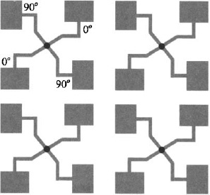
Figure 4.1. Circularly polarized 4 × 4 array made from linearly polarized elements. Four patches are combined to form a circularly polarized subarray.
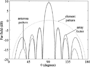
Figure 4.2. Element pattern superimposed on the array pattern and array factor.
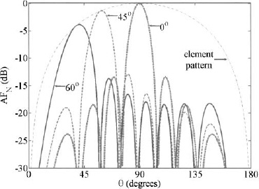
Figure 4.3. Element pattern superimposed on the array patterns when the array factor is steered to 90°, 60°, and 45°. The element pattern has a peak of 0dB. The array patterns are normalized to the broadside peak.
Hertzian dipoles are the simplest antenna elements outside of point sources. They are linearly polarized and have a pattern that is proportional to sin θ when oriented in the z direction. Placing several of these dipoles in the vicinity of each other causes the dipoles to interact. In other words, the dipoles all radiate and receive time-varying fields from each other. This interaction is called mutual coupling. Although mutual coupling is very important in antenna design, we will ignore it until Chapter 6. A first approximation to the electric field of an array of Hertzian dipoles is
We are interested in the relative electric field as a function of angle. Thus, the constants can be ignored and the approximation Rn ≈ r is valid in the denominator. Also, the Rn in the phase term can be approximated as shown in Chapter 2. The resulting far-field pattern for an array of Hertzian dipoles is

Figure 4.4. An 8-element array along the x axis with d = λ/2, (a) Isotropic point sources. (b) z-directed Hertzian dipoles.
The sin θ term is the relative shape of the far-field pattern of the Hertzian dipole, and the summation terms are the array factor.
An 8-element linear array lying along the x axis with d = λ/2 has the array factor shown in Figure 4.4a. This array factor has no polarization, because point sources have no polarization. Its directivity is 9.0 dB. The peak occurs at ![]() = 90° for all θ. Replacing the point sources with z-directed Hertzian dipoles having a directivity of 1.76 dB results in the array factor in Figure 4.4b. This antenna pattern is θ-polarized with no radiation in the z direction, because the element pattern has a null in that direction. The directivity of this array is 11.9dB and can be calculated using numerical integration of the array factor times the element pattern or the formula [4]:
= 90° for all θ. Replacing the point sources with z-directed Hertzian dipoles having a directivity of 1.76 dB results in the array factor in Figure 4.4b. This antenna pattern is θ-polarized with no radiation in the z direction, because the element pattern has a null in that direction. The directivity of this array is 11.9dB and can be calculated using numerical integration of the array factor times the element pattern or the formula [4]:
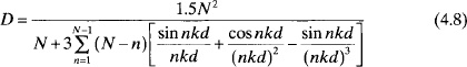
If d = λ/2, then this formula reduces to


Figure 4.5. An 8-element array along the z axis with d = λ/2. (a) Isotropic point sources. (b) z-directed Hertzian dipoles.
The directivity of the Hertzian dipole array is 2.9 dB higher than the directivity of the array factor, because the Hertzian dipole enhances the array factor main beam at θ = 90° and produces a null at θ = 0°. This example shows that the directivity of the array factor times the directivity of the element pattern does not have to equal the directivity of the array. In fact, in this case, the directivity of the element times the directivity of the array factor is less than the directivity of the array.
If the same z-directed Hertzian dipoles were placed along the z axis instead, would the directivity and antenna patterns be different? The answer is yes. An 8-element linear array lying along the z axis with d = λ/2 has the array factor shown in Figure 4.5a. Like the point source array along the x axis, this array has no polarization. Its directivity is also 9.0 dB. The peak occurs at θ = 90° for all ![]() . The array factor is identical to Figure 4.4a, except turned on its side. Replacing the point sources with z-directed Hertzian dipoles changes the array factor to look like Figure 4.4b. The antenna pattern is θ-polarized with no radiation in the z direction and has a directivity of 9.2 dB calculated using numerical integration or the formula [4]:
. The array factor is identical to Figure 4.4a, except turned on its side. Replacing the point sources with z-directed Hertzian dipoles changes the array factor to look like Figure 4.4b. The antenna pattern is θ-polarized with no radiation in the z direction and has a directivity of 9.2 dB calculated using numerical integration or the formula [4]:

If d = λ/2, then this formula reduces to
This pattern does not differ much from its array factor, so it has nearly the same directivity.
Even though the Hertzian dipole array in Figure 4.4 has the same number and type of elements as the Hertzian dipole array in Figure 4.5, its directivity is 2.7 dB higher. Unlike with point sources, the orientation of the element relative to the array has a significant effect on the directivity and antenna pattern of the array.
Example. Calculate the antenna pattern for a 1 × 8 array of z-oriented Hertzian dipoles along the x axis with element spacing λ. Repeat the example for z-directed Hertzian dipoles along the z axis.
Figure 4.6a shows the antenna pattern for the array along the x axis. The main beam is narrow in the x–y plane. The grating lobes point along the x axis. A null occurs in the main beam along the z axis. The directivity is reduced to 10.4 dB from Figure 4.4 due to the formation of two grating lobes at θ = 90° and ![]() = 90° and 270°. Figure 4.6b shows the antenna pattern for the array along the z axis. The main beam is omnidirectional in the x–y plane. Grating lobes do not appear at θ= 0° and 180°, because the element pattern has nulls in the z direction. The directivity is 11.7 dB. In this case, the array along the z axis has a greater directivity than the array along the x axis, because the element pattern nulls cancel the grating lobes at θ = 0° and 180°. Steering the main beam would cause the grating lobes to appear, because they would move out of the element pattern nulls.
= 90° and 270°. Figure 4.6b shows the antenna pattern for the array along the z axis. The main beam is omnidirectional in the x–y plane. Grating lobes do not appear at θ= 0° and 180°, because the element pattern has nulls in the z direction. The directivity is 11.7 dB. In this case, the array along the z axis has a greater directivity than the array along the x axis, because the element pattern nulls cancel the grating lobes at θ = 0° and 180°. Steering the main beam would cause the grating lobes to appear, because they would move out of the element pattern nulls.

Figure 4.6. An 8-element array of z-directed Hertzian dipoles with d = λ. (a) Along the x axis, (b) Along the z axis.

Figure 4.7. An 8-element array of z-directed Hertzian dipoles with d = λ/2 along the x axis. The beam is steered to ![]() = 90°, 45°, and 30°.
= 90°, 45°, and 30°.
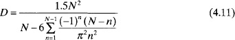
The main beam of the array in Figure 4.4 can be steered to an angle ![]() s in the x–y plane. Figure 4.7 shows the H-plane cut of the beam steered to
s in the x–y plane. Figure 4.7 shows the H-plane cut of the beam steered to ![]() = 90°, 60°, and 45°. Even though the element pattern is omnidirectional in the x–y plane, the peak of the main beam decreases, because the projected area of the rectangular area containing the dipoles decreases. As a result, the directivity decreases from 11.9dB at
= 90°, 60°, and 45°. Even though the element pattern is omnidirectional in the x–y plane, the peak of the main beam decreases, because the projected area of the rectangular area containing the dipoles decreases. As a result, the directivity decreases from 11.9dB at ![]() = 90° to 11.0dB at
= 90° to 11.0dB at ![]() = 60° and to 10.3 dB at
= 60° and to 10.3 dB at ![]() = 45°. Figure 4.8 shows the E plane cut of the main beam of the Hertzian dipole array in Figure 4.5 steered to
= 45°. Figure 4.8 shows the E plane cut of the main beam of the Hertzian dipole array in Figure 4.5 steered to ![]() = 90°, 60°, and 45°. The element pattern directivity decreases with decreasing θ, but the antenna pattern decreases only from 9.2dB at
= 90°, 60°, and 45°. The element pattern directivity decreases with decreasing θ, but the antenna pattern decreases only from 9.2dB at ![]() = 90° to 9.1 dB at
= 90° to 9.1 dB at ![]() = 60° and to 9.0dB at
= 60° and to 9.0dB at ![]() = 45°.
= 45°.
4.2. WIRE ANTENNAS
Hertzian dipoles and small loops serve as building blocks for larger wire antennas that have more directivity and are easier to match to the feed network.
4.2.1. Dipoles
Unlike Hertzian dipoles, long dipoles have current variations along the wire, so the constant current approximation is not valid. Since the dipole is narrowband and a standing wave exists along the wire, the current can be reasonably represented by a sinusoiod. Substitute I(z) = Iz sin[k(Lz / 2 ± z′)] into the equation for the magnetic vector potential to get
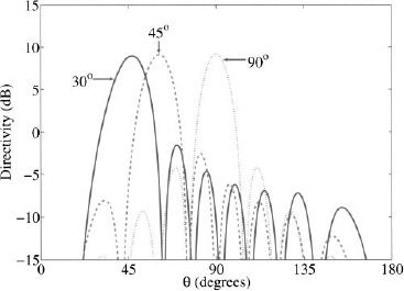
Figure 4.8. An 8-element array of z-directed Hertzian dipoles with d = λ/2 along the z axis. The beam is steered to θ = 90°, 45°, and 30°.
Begin solving this integral by breaking it into two parts and approximating the denominator by R ≅ r and the numerator by R ⋍ r – z′ cos θ.

Performing the integrations and simplifying results in
Next, the normalized electric field can be found from Az

When Lz = λ/2, then the directivity is 1.64 or 2.1 dB.

Figure 4.9. Hexagonal array with dipole elements in a square lattice. (Courtesy of the National Electronics Museum.)
Figure 4.9 is a hexagonal array of dipoles in a square lattice. This array was part of the Molecular Electronics for Radar Applications (MERA) project started by the U.S. Air Force (USAF) in 1964 as an exploratory development effort to examine the concept of implementing an X band all solid-state radar [5].
Example. Find the normalized electric field of a half-wavelength dipole. Substituting Lz = λ/2 into (4.15) results in
The input impedance of a dipole is a function of its length and diameter and is derived in Chapter 6. For a thin, resonant dipole that is slightly less than λ/2 long, the input impedance is about 73 Ω.
Crossed dipoles are frequently used to create an element with polarization diversity. One dipole controls the electric field parallel to it, and the orthogonal dipoles control the electric fields parallel to them. Varying the amplitude and phase of the signal at each dipole modifies the electric field amplitude and phase in orthogonal directions resulting in any polarization from linear through elliptical to circular [6]. The relative amplitude and phase of the two dipoles also determines its gain pattern.
In order to find the directivity and polarization of the crossed dipoles, the electric fields are calculated from the currents on the dipoles. If the dipoles are assumed to be short (Lx and Ly ![]() λ), then the crossed dipole current is the sum of the constant currents on each short dipole.
λ), then the crossed dipole current is the sum of the constant currents on each short dipole.
Substituting this current into the equation for the magnetic vector potential for a short dipole yields
where r is the distance from the origin to the field point at (x, y, z), Lx,y is the dipole length in the x and y directions, and Ix,y is the constant current in x and y directions. In the far field, the electric field in rectangular coordinates is found from the magnetic vector potential by
The transmitted electric field is given by
![]()
Converting this rectangular form of the electric field into spherical coordinates produces the relative far-field components [7]
The directivity is given by
If the polarization of the incident wave is written in spherical coordinates, then the polarization loss factor is [7]
where 0 ≤ PLF ≤ 1 with PLF = 1 a perfect match. The t and r subscripts represent transmit and receive, respectively.
Example. Calculate the currents needed to produce linear and circular polarization for crossed dipoles.
The results are shown in the following table:

The High-Frequency Active Auroral Research Program (HAARP) conducts upper atmospheric research in Alaska [8]. The HF transmitter delivers 3.6 MW to a rectangular planar array of 180 crossed dipole elements pointing at the sky. The transmitted signal is partially absorbed in a small volume a few hundred meters thick and a few tens of kilometers in diameter at an altitude between 100 and 350km (depending on operating frequency). Observations provide new information about the dynamics of plasmas in the ionosphere and new insight into solar–terrestrial interactions. Figure 4.10 is a picture of the HAARP transmit array laid out in a square grid. A tower holds each pair of crossed dipoles above the earth. The crossed dipoles permits control over the polarization of the transmitted signal.
A monopole is one arm of a dipole antenna placed orthogonal to a ground plane. The ground plane acts like a mirror and forms an image of the arm, thus creating a complete dipole. If the ground plane is infinite, the element pattern only exists when 0 ≤ θ 90°. A monopole above an infinite, perfectly conducting ground has a normalized element pattern given by
The quarter-wavelength monopole above an infinite ground plane has a directivity of D = 3.28 at θ = 90°. The input impedance of a monopole is about half that of a dipole [9]. Decreasing the size of the ground plane causes the peak of the directivity to decrease in angle from θ = 90° [10]. Monopoles are used in AM and FM broadcast antenna arrays. A three element broadcast array is shown in Figure 4.11.
An alternative to modifying the element weighting or spacing to obtain low sidelobes is to individually rotate the elements [11]. Rotating the elements changes the gain and polarization of the element pattern in a given cut of the antenna pattern. The change in gain can be accounted for in the element pattern, but the polarization must be taken into account by multiplying by the element polarization. For instance, a uniform array of dipoles in the x–z plane that are tilted from the z axis have an array far-field pattern given by
Figure 4.10. Photograph of the HAARP array of crossed dipoles. (Courtesy of HAARP.)

Figure 4.11. Photograph of a 3-element broadcast array in Altoona, PA.
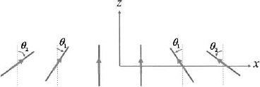
Figure 4.12. Orientation of the dipoles in a 3-element array.

The rotation of the elements is demonstrated with the four center elements of a linear dipole array in Figure 4.12. The two center elements are oriented to receive θ polarization. Elements at symmetric locations about the center of the array are mirror images of each other. Currents for the co-polarization all flow in the same direction and add in phase. The cross-polarized currents, on the other hand, flow in opposite directions in order to place a null in the cross-polarization pattern at boresight.
Assume that a linear array of dipoles lies along the x axis and in the x–z plane. The primary cut for the array antenna pattern is in the x–y plane. If the dipoles are parallel to the z axis, then the element pattern in the x–y plane is isotropic (ignoring mutual coupling), and the polarization is ![]() . If the dipoles are parallel to the x axis, then the element pattern in the x–y plane is cosineshaped and the polarization is
. If the dipoles are parallel to the x axis, then the element pattern in the x–y plane is cosineshaped and the polarization is ![]() . Tilting the dipole from the z-axis transitions its element pattern in the x–y plane from isotropic to cosine. The variations of the gain patterns due to element tilt alone provides some control over the amplitude of the signal received by an element from an off-boresight angle. The polarization of the rotated element plays an important role in determining the strength of the received signal. The power received by an element is multiplied by a polarization efficiency to account for the polarization mismatch between an incident wave and an antenna’s receive polarization. Figure 4.13 shows the θ-polarization gain patterns for a dipole rotated 0°, 45°, 60°, and 75° from the z axis. The overall θ-gain decreases with tilt angle. Also, the element pattern becomes less isotropic as θ increases. The change in gain due to element rotation should be enough to create a low-sidelobe taper for a given cut of the antenna pattern.
. Tilting the dipole from the z-axis transitions its element pattern in the x–y plane from isotropic to cosine. The variations of the gain patterns due to element tilt alone provides some control over the amplitude of the signal received by an element from an off-boresight angle. The polarization of the rotated element plays an important role in determining the strength of the received signal. The power received by an element is multiplied by a polarization efficiency to account for the polarization mismatch between an incident wave and an antenna’s receive polarization. Figure 4.13 shows the θ-polarization gain patterns for a dipole rotated 0°, 45°, 60°, and 75° from the z axis. The overall θ-gain decreases with tilt angle. Also, the element pattern becomes less isotropic as θ increases. The change in gain due to element rotation should be enough to create a low-sidelobe taper for a given cut of the antenna pattern.
Figure 4.14 a is a diagram of a 10 × 10 dipole planar array in the x–z plane with the dipoles parallel to the z axis. The array is θ-polarized with no cross-polarized pattern. The element spacing is dx = λ/2 and dz = λ/2. It has a gain of 22 dB with a relative sidelobe level of 13.1 dB.

Figure 4.13. Theta gain pattern in the x–y plane for dipoles tilted 0°, 45°, 60°, and 75° from the z axis.

Figure 4.14. A 10 × 10 θ-polarized planar array located in the x–z plane, (a) Before optimization, (b) After optimization.
Through the use of a genetic algorithm, the dipole tilt angles were found to minimize the maximum sidelobe level. The cost function calculates the copolarization and cross-polarization antenna patterns over the range of ![]() = 0° to
= 0° to ![]() = 90° and θ = 0° to θ = 90°. First, the co-polarization maximum sidelobe level is found. Second, the maximum of the cross-polarization pattern is found. The cost is then the larger of the two values. This results in the co-polarization maximum sidelobe level equaling to the cross-polarization maximum gain with the main beam oriented at
= 90° and θ = 0° to θ = 90°. First, the co-polarization maximum sidelobe level is found. Second, the maximum of the cross-polarization pattern is found. The cost is then the larger of the two values. This results in the co-polarization maximum sidelobe level equaling to the cross-polarization maximum gain with the main beam oriented at ![]() = θ = 90°.
= θ = 90°.
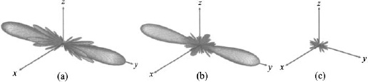
Figure 4.15. Array gain, (a) No optimization, (b) Optimized θ-gain. (c) Optimized ![]() -gain.
-gain.
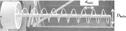
Figure 4.16. Diagram of a helical antenna. (Courtesy of ARA Inc. / Seavey Engineering.)
The optimized element rotations in a 10 × 10-element array are shown in Figure 4.14b. The gain is 19.9 dB with a maximum relative sidelobe level of 19.4 dB. Figure 4.15a is the θ-polarized gain before optimization and there is no cross-polarization. The optimized θ-polarized gain is shown in Figure 4.15b with the cross-polarization in Figure 4.15c. Since the currents on the dipoles have an x component as well as a z component, the pattern has both θ and ![]() components. The gain of the optimized array decreased by 2.1 dB, and the maximum sidelobe level decreased by 6.3 dB.
components. The gain of the optimized array decreased by 2.1 dB, and the maximum sidelobe level decreased by 6.3 dB.
4.2.2. Helical Antenna
A helical antenna looks like a corkscrew (Figure 4.16). The loops are considered very small and closely spaced when [12]
where Dhelix is the diameter of loop, dhelix is the spacing between loops, and Nhelix is the number of loops. If this condition is met, then the helical antenna acts like a monopole with a doughnut-shaped radiation pattern and is said to operate in the normal mode [12], where normal means that the maximum gain is perpendicular to the axis of the helix. The advantage of a normal mode helix is that it behaves like a monopole but is shorter at the same frequency. Its radiation resistance is given by
When the loops and spacing get larger, the helical antenna looks and acts like an end-fire array of loop antennas. In an array, the helical antenna radiates in the axial mode (along the axis of the helix) with a peak at θ = 0°. It works best when dhelix ≈ λ/4 and KDhelix = 2. The normalized electric field radiated by an axial mode helical antenna is [13]
where ψ = kdhelix ![]() . It has a peak directivity at a wavelength of λ0 given by [14]
. It has a peak directivity at a wavelength of λ0 given by [14]
Axial mode helical antennas are elliptically polarized with an axial ratio of [12]
The helical antenna is right-hand polarized when the helix increases in the counter clockwise direction when looking from the end toward the feed. The helix in Figure 4.16 is left-hand circularly polarized. Figure 4.17 shows a plot of the total electric field radiated by a helical antenna with Nhelix = 6, dhelix = 0.25λ, and Dhelix = λ/π. The directivity is 9.9 dB using (4.29) and 9.8 dB using numerical integration of (4.28). The input impedance of an axial fed helix is [12]

Figure 4.17. Total electric field of a helical antenna with Nhelix = 6, dhelix = 0.25λ, and Dhelix = λ/π.

Figure 4.18. Photograph of a quad helix array. (Courtesy of ARA Inc./Seavey Engineering.)
Helical antennas are frequently used for space communications systems where circular polarization is required. Figure 4.18 is a quad helix array (ARA/Seavey Model Number 9106-800) that operates from 405 to 450 MHz. It has a gain of 18dBic (dB above an isotropic point source with the same circular polarization). The array is 157.5 cm2 and 185.5 cm tall.
Example. Plot the three-dimensional antenna pattern for for an 8-element array of z-directed helical antennas with element spacing λ/2 along the x axis. The helical antenna has Nhelix = 6, dhelix = 0.25λ, and Dhelix = λ/π.
Figure 4.19 is a plot of the antenna pattern in decibels. The directivity of 16.3 dB is found by substituting (4.28) into (4.5) and numerically integrating. The helical antenna has the advantage of high directivity while still fitting into the λ/2 element spacing grid.

Figure 4.19. Array factor times element pattern (in decibels) for an 8-element array with element spacing λ/2 along the x axis. The element pattern is shown in Figure 4.17.
4.3. APERTURE ANTENNAS
An aperture antenna is typically a hole in a waveguide. The hole may be a slot in the side or the open end. A horn extends the size of the open end of the waveguide in order to increase the gain of an open ended waveguide. The input impedance is normally 50 Ω. Reflector and microstrip antennas are frequently categorized as aperture antennas as well. The gain of the horn or open-ended waveguide can be significantly increased by placing it at the focal point of a reflector to create another common type of aperture antenna.
4.3.1. Apertures
An L × W rectangular slot lying in the x–y plane (Figure 4.20a) has normalized far-field components given by [15]

Figure 4.20. Slots in the x–y plane centered at the origin. (a) Rectangular. (b) Circular.
where

The directivity is proportional to the area of the slot in wavelengths squared.
A plot of the total field, ![]() , radiated by a slot with L = 0.5λ and W = 0.1λ is shown in Figure 4.21. This small slot has a directivity of –2dB.
, radiated by a slot with L = 0.5λ and W = 0.1λ is shown in Figure 4.21. This small slot has a directivity of –2dB.
Slot elements can be circular as well. A circular slot of radius rc that is lying in the x–y plane (Figure 4.20b) with a uniform aperture field has far-field components given by
The directivity is based on the aperture area

Figure 4.21. Total electric field of a rectangular slot with a = 0.5λ and b = 0.1λ.
A plot of the total field radiated by a circular slot with rc = 5λ is shown in Figure 4.22. Its directivity is 30 dB.
Example. Find the antenna pattern of a 4-element linear array of reflector antennas that have a diameter of 10λ. Assume the edges of the reflectors touch.
First approximate the reflector apertures by a uniform circular slot. A plot of the three-dimensional directivity pattern appears in Figure 4.22. An individual element in the array has a directivity of 30 dB as calculated from (4.38). A 4-element array has a directivity of 36 dB. In this case, the directivity of the element times the directivity of the array factor equals the directivity of the array of elements. Figure 4.23 are the E- and H-plane antenna pattern cuts for this array. Since the phase centers are separated by 10λ, grating lobes in the array factor occur at θg = ±5.7°, ±11.5°, ±17.5°, ±23.6°, ±30°, ±36.9°, ±44.4°, ±53.1°, ±64.1°, and ±90°. These angles correspond to every third sidelobe rising above its surrounding sidelobes. The element pattern nulls occur close to the peak of the grating lobes, thus lowering the peak of the grating lobes.
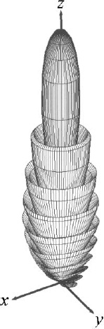
Figure 4.22. Total electric field (in decibels) radiated by a l0λ-diameter circular aperture.
The Very Large Array (VLA) is a radio telescope in New Mexico built from 27 dish antennas that are 25 m in diameter (Figure 4.24) [16]. Elements are placed in a Y-shape as shown in Figure 4.25. The size of the array is regularly changed by moving the elements along a railroad track. There are four configurations with maximum width of 36 km, 10km, 3.6km, or 1km. This array operates from 73 MHz up to 50 GHz. Table 4.1 lists the frequencies of operation and the resolutions associated with various configurations of the VLA.
The impedance of a thin slot antenna can be found from the impedance of a complementary dipole using Booker’s relation given by [17]
where Zdipole = Rdipole + jXdipole. Thus, when the dipole is capacitive, the slot is inductive, and when the dipole is inductive, the slot is capacitive. Lengthening a dipole makes it more capacitive, whereas lengthening a slot makes it more inductive.
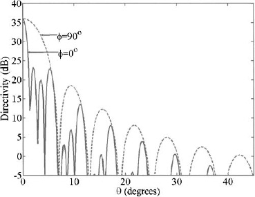
Figure 4.23. Principal cuts of the array factor times element pattern (in decibels) for a linear array with 4 elements spaced 10λ apart along the x axis. The element pattern is shown in Figure 4.22.

Figure 4.24. One reflector element of the VLA. (Courtesy of NRAO / AUI / NSF.)

Figure 4.25. Y-shaped VLA configuration. (Courtesy of NRAO / AUI / NSF.)
TABLE 4.1. Operating Characteristics of the VLA [16]

4.3.2. Open-Ended Waveguide Antennas
The metallic rectangular waveguide in Figure 4.26 has a wave propagating in the z direction and standing waves in the x and y directions. A propagating wave is either TE (transverse electric) with Ez = 0 or TM (transverse magnetic) with Hz = 0. Propagating waves are represented by complex exponential functions, whereas standing waves are represented by trigonometric functions. The wave vector has x, y, and z components and they are related by
The wavenumber in the x direction is given by

Figure 4.26. Rectangular waveguide.
and the wavenumber in the y direction is given by
The propagating wave constant is found from (4.40)
In order for a wave to propagate, kz must be real. If it is imaginary, then the wave is evanescent. In other words, it has an exponential decay as it travels down the waveguide. The apparent wavelength of the propagating wave in the z direction is λz or more commonly referred to as the waveguide wavelength, λg. Waves will propagate whenever (4.43) is greater than zero.
This occurs when the frequency exceeds the cutoff frequency found from (4.44).
When f > fcmn, then the wave propagates in the z direction; otherwise the wave attenuates in the z direction.
The normalized electric fields in the waveguide for a TE wave have a two-dimensional Fourier series representation given by
and for the TM wave we have

Example. Consider a length of air-filled copper X-band waveguide, with dimensions a = 2.286 cm, b = 1.016 cm. Find the cutoff frequencies of the first few propagating modes.
The cutoff frequencies are found from (4.45).
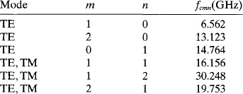
The TE10 mode is the dominant mode in the rectangular waveguide, since it has the lowest cutoff frequency. It has a normalized electric field at the opening given by
The expressions in (4.32) and (4.33) only apply when the field in the aperture is uniform. For the case when the aperture field is given by (4.48), the normalized far field expressions for the open-ended waveguide are [15]
where X and Y are given by (4.34). The directivity of the open-ended waveguide is [15]
Figure 4.27 is a plot of the antenna pattern for an 8 × 8 element planar array of open-ended waveguides operating in the TE10 mode. The directivity is 20.5 dB which is less than the directivity of the element pattern times the array factor (4.1 dB + 18.6dB = 22.7dB). The beamwidth is smaller and there are more sidelobes in the x direction compared to the y direction, because the waveguides in the x direction are 0.763λ wide while in the y direction they are 0.34λ wide. Thus, the element spacing in the x and y directions equals the width of the waveguide in those directions. A uniform aperture the same size as this array has a directivity of 23.2 dB.
Example. Plot the antenna pattern in Figure 4.27 with the beam steered to (θs, ![]() s) = (30°, 0°).
s) = (30°, 0°).
Figure 4.28 shows the pattern. The directivity is reduced to 20.5 dB due to the emergence of the grating lobe at (θ, ![]() ) = (53°, 180°).
) = (53°, 180°).
Open-ended waveguides are almost never used in an array except for a small array feeding a reflector antenna. As an example, Figure 4.29 shows a 4-element waveguide feed for the RARF (Reflected Array Radio Frequency) used in AN/APQ-140 Radar [18].

Figure 4.27. Array factor times the element pattern (in decibels) of an 8 × 8 element planar array of open-ended waveguides.

Figure 4.28. Antenna pattern in Figure 4.27 when steered to (θs, ![]() s) = (30°, 0°).
s) = (30°, 0°).

Figure 4.29. Waveguide feed for the RARF. (Courtesy of the National Electronics Museum.)
Circular waveguides are also used as elements in arrays. The Electronically Agile Radar (EAR) had 1818 circular waveguide elements [19]. A ceramic loaded circular waveguide element connected to a phase shifter is inserted into each circular waveguide hole in the array backplane (Figure 4.30).

Figure 4.30. The EAR with a blowup of the element/phase shifter module. (Courtesy of the National Electronics Museum.)
4.3.3. Slots in Waveguides
Slots are placed in the waveguide walls in order to couple a small portion of the fields in and out of the waveguide. Slot resonance (susceptance equals zero) is a function of the slot size and occurs when 2L + 2W ≈ λ[22]. As with a dipole, increasing the slot width increases the bandwidth of the slot. Slot admittance is a function of the placement of the slot on the waveguide. Slots can be on either the broad or narrow walls and are positioned to have the desired admittance which in turn causes the field radiated by the slot to have the desired amplitude and phase. The admittance or impedance of a slot depends upon its displacement from the centerline (Δ) and its tilt (ζ) as shown in Figure 4.31. The narrow wall of a rectangular waveguide is too short for a rectangular resonant slot, so either a different slot shape that fits on the wall must be used (like the barbell shape in Figure 4.31), or the slot extends into the broad wall of the waveguide. Examples of the two most commonly used slots in array antennas are shown in Figure 4.32. The field at the slots in the broad wall of the waveguide in Figure 4.32a are controlled by the element offset, Δ, from the centerline. The field at the slots in the narrow wall of the waveguide in Figure 4.32b are controlled by the element tilt, ζ. Note that the tilted slot in the narrow wall wraps around the edge so that there is a small notch in the top and bottom broadside walls as seen in Figure 4.33. A long slot at the center of the broad wall or a vertical slot in the side wall does not radiate. Longitudinal slots in the broad wall of the waveguide have negligible cross-polarization. Slots have a cross-polarization component when ζ ≠ 0. Longitudinal slots are not used in the side wall, because the admittance and power radiated cannot be controlled by changing their position in the y direction. Crossed slots radiate circular polarization if placed properly.

Figure 4.31. Slots in a rectangular waveguide.
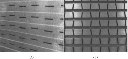
Figure 4.32. Examples of slots in a rectangular waveguide, (a) Offset longitudinal slots in the broad wall (AN/APG-68 radar antenna), (b) Inclined slots in the narrow wall (AWACS antenna). (Courtesy of the National Electronics Museum.)

Figure 4.33. Tilted slot in the narrow wall of a rectangular waveguide. (Courtesy of the National Electronics Museum.)
A resonant waveguide array is shorted on one end and fed on the other so that a standing wave results as shown by the current distribution (dark is higher amplitude) on a rectangular waveguide in Figure 4.34. The null (white spot) in the center of the broad wall occurs λ/4 behind the short. Slots should be placed such that they disturb the current distribution in such a way as to cause radiation. The current flow on both sides of the slot should be in the same direction. The first slot is placed at either λg/4 or λg/2 behind the waveguide termination.
At (x, y, z) = (a/2, b, λg/4) a null occurs in the standing wave (first white spot on top of the waveguide in Figure 4.34). Placing the center of a resonant slot at x = a/2 with its long side parallel to the z direction does not disturb the current flowing on the waveguide (Figure 4.35a). Rotating this slot to ζ = 30° while keeping the slot center at x = a/2 does not perturb the standing wave currents, so the slot does not radiate (Figure 4.35b). Moving the slot in the x direction causes a disruption of the current flow and the standing wave resulting in radiation. Figure 4.35c shows the slot at Δ = 0.1λ, and Figure 4.35d shows the slot at Δ = 0.2λ. Increasing Δ increases the power radiated by the slot. When the slot in the broadside wall that is parallel to the z axis is placed λg/4 behind the short, the power radiated by the slot is a function of Δ. Consequently, the elements near the center of a low-sidelobe array have a larger Δ than the elements near the edges.
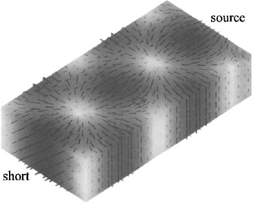
Figure 4.34. Currents on a rectangular waveguide when one end has a short.

Figure 4.35. Currents on a rectangular waveguide when the slot is λg/4 from the short. (a) Δ = 0, ζ = 0. (b) Δ = 0, ζ = 30°. (c) Δ = 0.1λ, ζ = 0. (d) Δ = 0.2, ζ = 0.
At (x, z) = (a/2, λg/2), a peak occurs in the standing wave. Placing the center of a resonant slot at x = a/2 with its long side parallel to the z direction does not disturb the current flowing on the waveguide, even though the current is at a peak, because the slot is so thin and the current is flowing in the z direction (Figure 4.36a). Rotating this slot to ζ = 30° while keeping the slot center at x = a/2 disrupts the current flow and causes radiation (Figure 4.36b). Moving the slot in the x direction produces little disturbance to the standing wave currents, thus no radiation (Figure 4.36c). Figure 4.36d shows the slot at ζ = 90° and blocking the flow of current in the z direction. When the slot is placed at λg/2 behind the short, the power radiated by the slot is a function of ζ.
Shunt slots interrupt the transverse currents (Jx and Jy) and can be represented by a two-terminal shunt admittance. Series slots interrupt Jz and can be represented by a series impedance. If a slot interrupts all three current components, then a Pi or T impedance network represents it. The following formulas were derived by [21][22][23]:
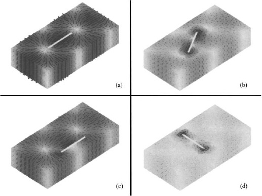
Figure 4.36. Currents on a rectangular waveguide when the slot is λg/2 from the short. (a) Δ = 0, ζ = 0. (b) Δ = 0, ζ = 30°. (c) Δ = 0.2, ζ = 0. (d) Δ = 0, ζ = 90°.
Longitudinal slot in broad face (shunt):
Slot in narrow face (shunt):
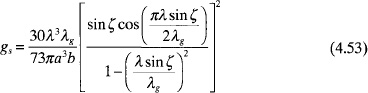
Traverse slot in broad face (series):
where gs is the normalized slot admittance, rs is the normalized slot resistance, Δ is the offset from waveguide centerline,
and ζ is the slot tilt angle (Figure 4.31).
The radiation pattern of a thin slot is the same as a dipole except it has the orthogonal polarization. A horizontal slot has vertical polarization, while a vertical slot has horizontal polarization.
Figure 4.37 is the 548-element planar array of slots used for the APG-68 radar system [24]. The elements are longitudinal slots in the broad side of the rectangular waveguide. The AN/APG-68 radar is a solid-state medium range (up to 150 km) pulse-Doppler radar designed for the USAF F-16.
4.3.4. Horn Antennas
A horn antenna increases the aperture size, hence the directivity, of an open-ended waveguide and provides a better match to free space. Figure 4.38 is a diagram of a rectangular horn antenna where the aperture is flared in two orthogonal directions. The flare in Figure 4.38 is linear, but it could also be exponential. If the flare of the horn is only in the direction of the electric field in a TE10 waveguide (A = a and B > b), then the horn is known as an E-plane sectoral horn. If the flare of the horn is only orthogonal to the direction of the electric field in a TE10 waveguide (A > a and B = b), then the horn is known as an H-plane sectoral horn. Flaring a horn in both directions (A > a and B > b) produces a pyramidal horn. The sectoral horns can be stacked along the narrow dimension to form a linear array. Since the horns are flared in the plane orthogonal to the array, the beam is also narrow in that plane. For analysis purposes, the E-plane is ![]() = π/2, and the H-plane is
= π/2, and the H-plane is ![]() = 0 in Figure 4.38.
= 0 in Figure 4.38.
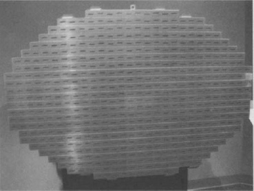
Figure 4.37. Photograph of the APG-68. (Courtesy of the National Electronics Museum.)

Figure 4.38. Diagram of a rectangular horn antenna.
Normalized expressions for the electric field of an E-plane sectoral horn antenna are [15]


The corresponding directivity is
Figure 4.39 is a plot of the electric field of an E-plane sectoral horn with a = 0.763λ, b = 0.34λ, A = 0.763λ, B = 3.6λ, and ρ2 = 7.6λ. It has a narrow beam in the E plane due to the flair of the horn. The normalized electric fields and directivity of an H-plane sectoral horn antenna are [15]
Figure 4.40 is a plot of the electric field of an E-plane sectoral horn with a = 0.763λ, b = 0.34λ, A = 4.6λ, B = 0.34λ, and ρ1 = 6.9λ. It has a narrow beam in the H plane due to the flair of the horn. The normalized electric fields and directivity of a pyramidal horn antenna are [15]
Figure 4.41 is a plot of the electric field of an E-plane sectoral horn with a = 0.763λ, b = 0.34λ, A = 4.6λ, B = 3.6λ, ρ1 = 6.9λ, and ρ2 = 7.6λ. Since the aperture is large in both directions, the beamwidth is narrow for all ![]() . Definitions for the variables in the field and directivity equations for the horns are listed below:
. Definitions for the variables in the field and directivity equations for the horns are listed below:
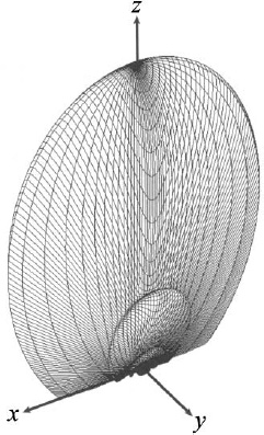
Figure 4.39. Total electric field radiated by a 0.76λ × 3.6λ E-plane sectoral horn.
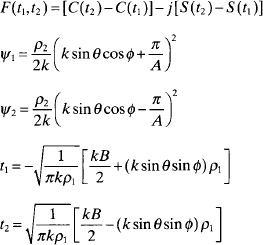
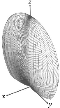
Figure 4.40. Total electric field radiated by a 4.6λ × 0.34λ H-plane sectoral horn.

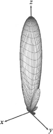
Figure 4.41. Total electric field radiated by a 4.6λ × 3.6λ pyramidal horn.

Pyramidal horns are not commonly used in arrays, because the horn flare in both directions means that the elements would be spaced far apart in the array and grating lobes would appear.
Example. Plot the antenna patterns for 8-element linear arrays of E-plane sectoral horns, H-plane sectoral horns, and pyramidal horns using the horn patterns in Figures 4.39 to 4.41.
A linear array of E-plane sectoral horns would be along the x axis. Assuming that the elements are placed side by side, then the element spacing would be dx = 0.763λ. Figure 4.42 shows the array pattern in decibels. A linear array of H-plane sectoral horns would be along the y axis. Assuming that the elements are placed side by side, then the element spacing would be dy = 0.34λ. Figure 4.43 shows the array pattern in decibels. A linear array of pyramidal horns along the x axis has an element spacing of dx = 4.6λ. This large spacing produces grating lobes that are obvious in the H-plane cut of the array pattern in Figure 4.44.
Figure 4.42. Array factor times element pattern (in decibels) for an 8-element array of E-plane sectoral horns with element spacing 0.76λ along the x axis. The element pattern is shown in Figure 4.39.
Figure 4.45 is a picture of a low sidelobe 80-element array of H-plane sectoral horns. The large air conditioning unit on the back of the array keeps the feed network and phase shifters at a constant temperature in order to minimize errors and keep sidelobes low. Figure 4.46 is a plot of the far-field sum pattern with a maximum relative sidelobe level of 31 dB. Figure 4.47 is a plot of the far-field difference pattern with a maximum relative sidelobe level of 28.5 dB. Each element had a 6-bit digitally controlled ferrite phase shifter.
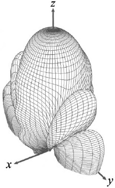
Figure 4.43. Array factor times element pattern (in decibels) for an 8-element array of H-plane sectoral horns with element spacing 0.34λ along the y axis. The element pattern is shown in Figure 4.40.

Figure 4.44. Principal cuts of the array factor times element pattern (in decibels) for a linear array with 8 pyramidal horn elements spaced 4.6λ along the x axis. The element pattern is shown in Figure 4.41.

Figure 4.45. Linear array of 80 H-plane sectoral horns.
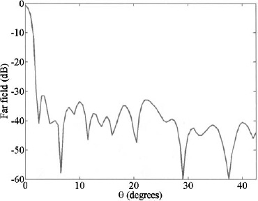
Figure 4.46. Far-field sum pattern of the 80-element array of H-plane sectoral horns.
4.4. PATCH ANTENNAS
A simple patch antenna consists of a flat, thin piece of metal in some geometric shape on top of a dielectric substrate with a metal ground plane on the bottom. Patches are very popular array elements because they
- Do not protrude from the surface.
- Can be cheaply made with the same technology as printed circuits.
- Integrate well with printed circuit boards.
- Are easy to conform to a nonplanar surface.
- Are rugged.

Figure 4.47. Far-field difference pattern of the 80-element array of H-plane sectoral horns.

Figure 4.48. Rectangular patch made from copper tape and polycarbonate. (Courtesy of Amy Haupt.)
The most common patch shape is a rectangle with a disk being second. Many other shapes, including fractal, have been explored as well. An example of a simple patch antenna is shown in Figure 4.48 [25]. The patch is made from a 10.3- by 10.5-cm piece of copper tape placed in the center of a 10.28- by 10.45-cm piece of thick polycarbonate (εr = 2.7) with a copper tape ground plane. Such a patch is very easy to build and has a very narrow impedance bandwidth of 54 MHz or 2.8% at 2.075 GHz (Figure 4.49).

Figure 4.49. S11 of the patch in Figure 4.48. (Courtesy of Amy Haupt.)

Figure 4.50. Some methods of feeding a patch antenna.
Patches can be fed in a number of ways. The left patch in Figure 4.50 is fed by a coaxial cable from beneath the ground plane. A hole is drilled through the ground, substrate and patch. Then the inner conductor of the coaxial cable is place in the hole and soldered to the top of the patch. The outer conductor is soldered to the ground plane. The hole in the ground plane must be big enough so that the inner conductor does not touch the ground plane. The center patch in Figure 4.50 is fed via a microstrip transmission line. Part of the patch is cut out to match the impedance of the patch to that of the transmission line. The patch on the right in Figure 4.50 is fed from below by an open-ended microstrip transmission line. This approach as well as aperture-fed patches require multilayered substrate boards.
Patches tend to be narrowband, so a variety of techniques have been developed to increase their bandwidth. The bandwidth o f a L × W rectangular patch on top of a substrate h thick and having a permittivity of εr has the following relationship [26]:

Figure 4.51. Techniques for increasing the bandwidth of a rectangular patch antenna.
where λ0 is the center frequency. The bandwidth of a patch can be increased by matching the patch to the feed line, adding extensions, placing pins connecting the patch to the ground plane in strategic locations, making the substrate thicker, decreasing the dielectric constant of the substrate, stacking patches, and adding parasitic patches (Figure 4.51) [27].
Polarization of the patch is controlled through the location of the feed, shape of the patch, slots in the patch, or shorting pins. There are two approaches to creating elliptically polarized patch antennas [28]. First, feed the patch at a single point and change the shape of the patch or place slots inside the patch. Second, feed the patch at two points so the amplitude and phase difference creates the desired polarization. In both cases, two modes are induced in the patch.
The normalized fields radiated by a rectangular microstrip patch are

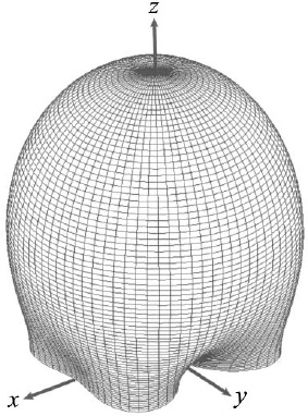
Figure 4.52. Total electric field of a microstrip patch.

where k0 is the wavenumber in free space. These formulas assume the patch consists of two radiating slots that are W wide and separated by a distance L. The directivity of a rectangular patch is estimated to be [15]
Figure 4.52 is a plot of the total electric field ![]() a 0.4λ × 0.4λ square patch.
a 0.4λ × 0.4λ square patch.
Example. Plot the antenna pattern for an 8- × 4-element planar array of patches (0.4λ × 0.4λ) with dx = dy = 0.5λ.
Figure 4.53 shows the array pattern.
An estimate of the dimensions of a rectangular patch are given by [28]
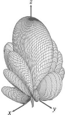
Figure 4.53. Array factor times the element pattern (in decibels) of an 8- × 4-element planar array of rectangular patches.
The input resistance at resonance is [15]
where
![]()

where

The microstrip array design in Figure 4.54a has a conical beam with a null at θ = 0° and a peak between θ = 0° and θ = 90° at 5.2GHz [29]. The conical beam results when the structure is not completely circularly symmetric but is self-congruent for rotations of ![]() = 360°/N, where N is the number of elements in the circular array. Both the currents on the microstrip patches and the electric field in the plane of the array are calculated using the finite difference time domain (FDTD) approach. The currents and electric field are shown in Figures 4.54b and 4.54c.
= 360°/N, where N is the number of elements in the circular array. Both the currents on the microstrip patches and the electric field in the plane of the array are calculated using the finite difference time domain (FDTD) approach. The currents and electric field are shown in Figures 4.54b and 4.54c.
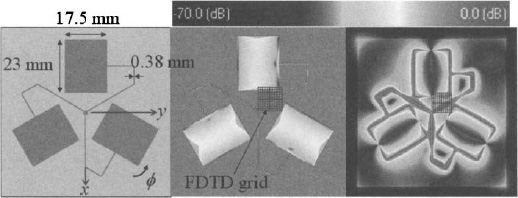
Figure 4.54. Conical beam antenna made from three patches, (a) Diagram. (b) Currents, (c) Electric field in the plane of the antenna. (Courtesy of Remcom.)
4.5. BROADBAND ANTENNAS
The bandwidth of a phased array is determined by a number of factors. As mentioned in Chapter 2, time delay units are needed to extend the array bandwidth when the main beam moves more than a half-beamwidth in any direction over the instantaneous bandwidth when steered to the maximum scan angle. Grating lobes due to large element spacing also limit the bandwidth at the highest frequency. Finally, the elements, feed network, and associated hardware must function appropriately over the bandwidth of the array. This section describes four types of broad band elements. Many other examples can be found in the literature [30].
4.5.1. Spiral Antennas
Spiral antennas have two or more arms that wrap around each other [31]. The arms of an Archimedian spiral in the x−y plane progressively move farther from the center with increasing ![]() . Arm n of an Narm arm Archimedean spiral is described by [32]
. Arm n of an Narm arm Archimedean spiral is described by [32]
where rin is the distance from the center to the start of an arm and
![]()
Usually, this antenna is complementary: The strip width equals the space between the strips (δs = δw). The input impedance of a complementary spiral is [33]
If the area between the arms is free space, then

Figure 4.55. Diagram of an Archimedian spiral antenna with its antenna pattern.
For a spiral antenna, the circumference of the circle that just contains the spiral is approximately equal to the maximum wavelength radiated by the spiral [34]. As such, the low frequency of operation is determined by the outer radius while the high frequency is determined by the inner radius or smallest dimension.
Figure 4.55 shows the far-field pattern of a 2-arm self-complementary Archimedian spiral at 1GHz with N = 4 turns. This element pattern was calculated numerically. The Archimedean spiral antenna radiates from a region where the circumference of the spiral equals one wavelength. This is called the active region of the spiral. Each arm of the spiral is fed 180° out of phase; so when the circumference of the spiral is one wavelength, the currents at complementary or opposite points on each arm of the spiral add in phase in the far field. Reflections from the end of the arm increase the lower end of the bandwidth predicted by (4.77). Placing loads at the end of the arms can reduce these reflections [35]. Figure 4.56 shows the extent of the current on the arms of the spiral as a function of frequency. At 250 MHz, the current (darker means higher amplitude) extends the length of the arms. As the frequency increases, the current extends less out the arms. The spiral has a very broad bandwidth as shown by the plot of the computed S11 in Figure 4.57.
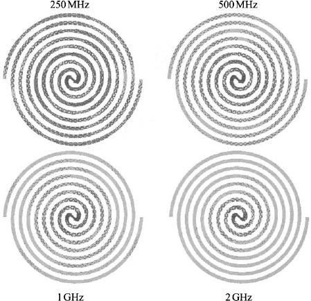
Figure 4.56. At 250 MHz, the Archimedian spiral antenna currents extend to the end of the arms. As the frequency increases, the current limits move closer to the center.
Spiral antennas radiate out both the front and back of the element. The back radiation is undesirable and may be reduced by placing the spiral above a ground plane, using a lossy cavity behind the spiral, or using a conical spiral. A ground plane is generally a bad idea, because it significantly reduces the spiral’s bandwidth. The lossy cavity is the most popular option, even though it adds depth to the spiral and induces loss in the element. A conical spiral is not conformal to the surface and is more difficult to manufacture [36].
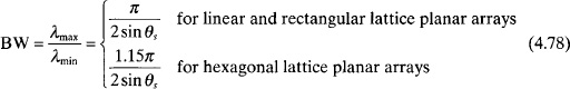
Placing this antenna in an array limits the diameter of the spiral to less than the element spacing. For a linear array or planar array with a rectangular lattice, grating lobes limit the maximum spacing between elements based on the steering angle to d = 0.5λmin/sin θs. The lower limit is based upon the diameter of the spiral which has to be less than the element spacing (d = λmax/π). As a result, the bandwidth of the array has an upper limit of

Figure 4.57. S11 of the Archimedian spiral antenna assuming a 250-Ω feed.
Example. Plot the antenna pattern for an 8-element array of spirals shown in Figure 4.55.
Figure 4.58 shows the array pattern.
Figure 4.59 is a photograph of one of the spiral antennas that was in a 4-element interferometer array on the Gemini spacecraft. This array was part of the rendezvous radar in the recovery section of the spacecraft. It located and tracked the target vehicle during rendezvous maneuvers. The array/interferometer consisted of four spirals: one each for transmit, reference, elevation, and azimuth.
Two identical linear arrays of Archimedean spiral elements operating at the same frequency but having orthogonal polarizations can be interleaved such that they have low sidelobes [37], Each self-complementary spiral has five turns and is 34 mm in diameter. They are center-fed with a 1-V sources. The design specifications include ±30° scan with an axial ratio (AR) less than 3dB, a VSWR less than 2, and a relative sidelobe level (RSLL) under −10 dB from 3 GHz to 6 GHz. The 80-element array has 40 RHCP spirals and 40 LHCP spirals. The spirals have a center-to-center separation of 38 mm, so the grating lobes start around 3.94 GHz.
Figure 4.60 shows a plot of the axial ratio of the array for three steering angles. The AR shows little variation as a function of steering angle and is under 3 dB above 4 GHz for all steering angles.

Figure 4.58. Computed far-field pattern of an 8-element linear array of Archimedian spirals along the x axis with d = 0.55λ.
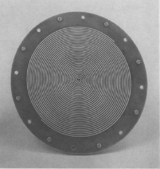
Figure 4.59. Picture of a spiral element for the Gemini rendezvous radar. (Courtesy of the National Electronics Museum.)
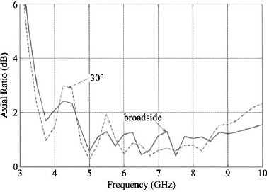
Figure 4.60. Axial ratio of the array at four beam pointing directions.

Figure 4.61. Plot of the VSWR at four beam pointing directions.
Element 20 has the worst VSWR when connected to a 250-Ω feed line. Figure 4.61 shows that the VSWR rapidly decreases until 2.5 GHz. There is a small resonance at 3.25 GHz when the beam is steered to 20° or 30°. The VSWR bandwidth extends from 2.75 GHz to greater than 10 GHz (except around 3.25 GHz, but this exception only occurs for element 20).
Figure 4.62 shows the maximum RSLL for an optimized 80-element array, with 40 RHCP spirals and 40 LHCP spirals. This maximum RSLL is shown for various steering angles, up to 30°. At broadside, the RSLL stays under –11 dB until 7 GHz (maximum frequency of the simulation). For the other steering angles, it remains under –10 dB until 5.25 GHz (theory gives 5.26 GHz), the frequency at which the grating lobe appears at a 30° steering angle. Whatever the steering angle, the RSLL is quite flat. This is obviously due to the choice of the cost function.

Figure 4.62. Plot of the maximum RSLL at four beam pointing directions.
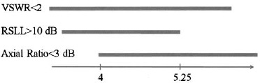
Figure 4.63. The array bandwidth defined three different ways.
If the bandwidth is defined simultaneously for a RSLL less than –10 dB, an AR less than 3 dB and a VSWR less than 2, all of this for steering angles from –30° to +30°, this array has an approximate bandwidth of 4–5.25 GHz, or 27%. Figure 4.63 shows the AR, VSWR, and RSLL bandwidths. This figure clearly shows that the AR establishes the lowest frequency in the bandwidth, while the RSLL sets the highest frequency. Array bandwidth may be a function of more than just impedance bandwidth of the element and the formation of grating lobes.

Figure 4.64. Some broadband dipole-like antennas. (a) Fat dipole. (b) Bicone. (c) Bicone with spherical caps. (d) Ellipsoidal.
4.5.2. Dipole-Like Antennas
A dipole antenna has a very narrow bandwidth because the current only resonates along the length of the dipole. Making the dipole fat (Figure 4.64a), encourages the currents to pursue other paths like circling the dipole, thus adding another dimension to the current flow and thereby broadening the bandwidth. Balanis notes that a dipole with a length-to-diameter ratio of 5000 has a 3% bandwidth, while one with a length-to-diameter ratio of 260 has a 30% bandwidth [15]. Another method of increasing the bandwidth of a dipole is to make each wire into a cone with the apex of the cones at the feed point (Figure 4.64a). This type of an antenna is called a biconical antenna. The bandwidth of a biconical antenna is further extended by adding spherical caps on the ends of the cones as in Figure 4.64c. Sharp edges cause radiation, so the spherical caps reduce the amount of radiation from the cone edge. Further smoothing creates ellipsoidal or spherical arms on the dipole (Figure 4.64d) [38].
Two-dimensional versions of these dipole-like antennas are broadband as well. For instance, the bow-tie antenna is a two-dimensional version of the bicone antenna [39], Circular caps are often placed at the end of the bow-tie antennas as well [39]. These antennas also come in monopole flavors too [40].
Example. Plot the antenna pattern for an 8- × 4-element planar array of y-oriented bow-tie elements (0.4λ × 0.4λ) spaced λ/2 apart in the x and y directions.
Figure 4.65 shows the element pattern and Figure 4.66 shows the array pattern. The array pattern is compressed in the y–z plane, because the element pattern is narrow in that direction and there are more elements in the y direction.
The broadband-printed bent dipole shown in Figure 4.67 has the S11 plot shown in Figure 4.68. This element has an S11 below –10 dB from 7.9 to 12.9 GHz which is a 48% bandwidth. The three-dimensional element pattern in Figure 4.69 has a directivity of 4.8 dB. If this element is placed in a 3 × 5 array with element spacing λ/2 in the x and y directions, then the product of the element pattern times the array factor is shown in Figure 4.70. This array pattern has a directivity of 16.6 dB at 10 GHz.

Figure 4.65. Diagram of a bow-tie antenna antenna with its antenna pattern.
Figure 4.66. Computed far-field pattern of pattern of an 8-element linear array along the x axis with d = 0.55λ.
4.5.3. Tapered Slot Antennas
A tapered slot antenna (TSA) or Vivaldi antenna [41] is a flared slot line just like a horn antenna is a flared waveguide. The TSA is an ideal wideband array element because [42]

Figure 4.67. Diagram of a broadband-printed bent dipole. (Courtesy of James R. Willhite, Sonnet Software, Inc.)

Figure 4.68. Plot of S11 for the element in Figure 4.67.
- The bandwidth with VSWR <2 can be up to 10:1.
- The cosθ element pattern exists over all scan planes out to θs = 50°−60°.
- No need to use lossy materials to obtain bandwidth.
- A balun can be easily incorporated into the design.
- Beamwidth remains constant over the operating bandwidth [43].
These advantages have led to the widespread use of TSAs in the design of new phased arrays.
Figure 4.71 is a picture of the AN/APG-81 phased array with over 1000 elements and a blowup of the slotted tab element that has a rectangular opening. Oftentimes the opening is a linear taper instead of a rectangular tab. Figure 4.72 is a diagram of a 10-GHz 50-Ω TSA with its antenna pattern. The slot line is 5 mm long and 1.39 mm wide on a 13.27–mm × 15.34–mm dielectric substrate (εr = 3) 2 mm thick. The aperture width is 5.67 mm. The reflection coefficient as a function of frequency is shown in Figure 4.73. It is below –10 dB from 9.2 to 11.4 GHz for a 22% bandwidth. The far-field pattern of an 8-element linear array along the x axis with d = 0.55λ is shown in Figure 4.74.

Figure 4.69. Element pattern for the broadband-printed bent dipole at 10 GHz.

Figure 4.70. Array pattern for a 3- × 5-element array.

Figure 4.71. Slotted tab element in the AN/APG-81 antenna array. (Courtesy of Northrop Grumman and available at the National Electronics Museum.)

Figure 4.72. Diagram of a tapered slot antenna with its antenna pattern.

Figure 4.73. Plot of S11 versus frequency for the TSA.

Figure 4.74. Far-field pattern pattern of an 8-element linear array along the x axis with d = 0.55λ.

Figure 4.75. Diagram of a Vivaldi antenna.
A curved opening provides a smoother transition to free space than the linear opening which increases the bandwidth. Optimizing the shape of the opening yields better performance [44], A typical Vivaldi design appears in Figure 4.75 [45]. Optimizing the exponential taper, length, and width of the slot along with the feeding mechanism produces excellent broadband elements. The feed design limits the high frequency of the bandwidth, whereas the aperture size limits the low frequency of the bandwidth. Some general guidelines for the design of a Vivaldi antenna array include [42]:
- dx, dy ≈ 0.45λ.
- Increasing the element length, lowers the minimum frequency in the bandwidth.
- Substrate:
- Its thickness should be ≈0.1 times the element width.
- Increasing εr lowers the minimum frequency in the bandwidth. It may also lower the maximum frequency as well.
- Increasing Ra lowers the minimum frequency in the bandwidth but increases variations in the impedance over the bandwidth.
- Increasing D increases the antenna resistance at lower frequencies.
Surrounding the TSA with shorting pins or vias that connect the top and bottom metal surfaces on either side of the substrate eliminates unwanted resonances that limit the bandwidth [46].
The Vivaldi antenna in Figure 4.76 is a Schaubert design [47] with L = 97 mm, W = 27.02mm, A = 18.6mm, D = 8.47 mm, and R = 0.03. The element spacing is dx = dy = 0.09λ at the lowest frequency of 1.0 GHz. The substrate is 3.15 mm thick and has a relative dielectric constant of 2.2. The slot line and strip line feed are 1.1 mm wide. The strip line feed has an input impedance of 50 Ω and narrows to 82 Ω. A picture of the element and the array are shown in Figure 4.76. This 144 element (9 × 8 × 2 pol) array operates from 1 to 5 GHz. The planar array consists of parallel linear arrays with each linear array printed on a single circuit board. An identical array is placed orthogonal to the first planar array in order to get the two orthogonal polarizations. The circuit boards have notches cut in them between each element in order to place them in an “egg crate assembly” as shown in Figure 4.76.
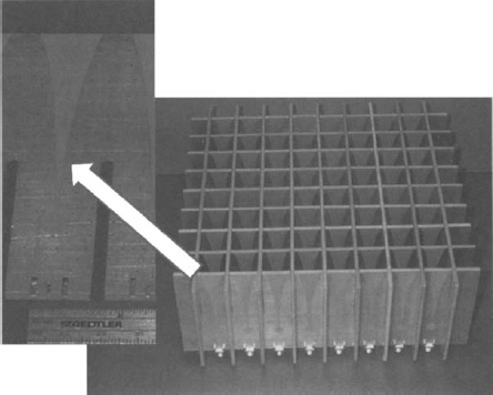
Figure 4.76. Vivaldi planar antenna array with close-up picture of element. (Courtesy of Daniel Schaubert, University of Massachusetts.)
Figure 4.77 is a picture of a Vivaldi element for the direction finding array in Figure 4.78 [48], The element has a receive bandwidth of 30MHz to 3 GHz and a transmit bandwidth at 1 kW of 100 MHz to 4 GHz. It is 88.9 cm by 42.2 cm and weighs only 4.7 pounds. The gain variation over the bandwidth is shown in Figure 4.79, and its beamwidth in the vertical and horizontal planes are shown in Figure 4.80.
4.5.4. Dielectric Rod Antennas
A dielectric rod antenna is formed from a piece of dielectric that extends from the open end of a waveguide. If the dielectric is polystyrene (a common type of plastic), then the antenna is called a polyrod. The radiation pattern of the polyrod is a function of its cross section, length, dielectric constant, and shape. A high dielectric constant results in a thinner and lighter rod, but a narrower bandwidth. Dielectric rod antennas commonly use a cylindrical waveguide with a shaped dielectric rod protruding from the waveguide as shown in Figure 4.81. To maximize directivity, the diameter of the dielectric rod should be [12]
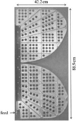
Figure 4.77. Vivaldi antenna array for DF array. (Courtesy of US Navy SPAWAR.)

Figure 4.78. DF array of Vivaldi elements. (Courtesy of US Navy SPAWAR.)

Figure 4.79. Measured gain of the Vivaldi element in Figure 4.77. (Data for plot courtesy of US Navy SPAWAR.)
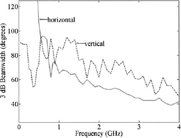
Figure 4.80. Measured beamwidths of the Vivaldi element in Figure 4.77. (Data for plot courtesy of US Navy SPAWAR.)
for L > 2λ and 2 < εr < 5. Cylindrical rods can be tapered to get a better match and reduce sidelobes. An approximate expression for the far field of a polyrod is [12]
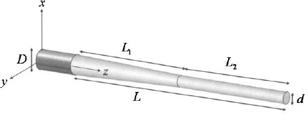
Figure 4.81. Polyrod antenna.

Figure 4.82. Antenna pattern cuts for the tapered and uniform polyrod antennas. A three-dimensional view of the tapered polyrod antenna is in the upper right-hand corner.
where ![]() .
.
Example. Calculate the far field radiated by the polyrod antenna shown in Figure 4.81 at 10 GHz with D = 0.5λ, d = 0.3λ, L = 6λ, L1 = 3λ, L2 = 3λ, and εr = 3 and for a uniform polyrod (d = 0.5λ).
Figure 4.82 shows the antenna pattern for a uniform polyrod antenna (dashed line) calculated using (4.80). No simple formula exists for calculating the antenna pattern of the tapered polyrod, so the pattern was numerically calculated using Microwave Studio. The tapered polyrod has lower maximum sidelobe levels at the expense of a decrease in directivity.
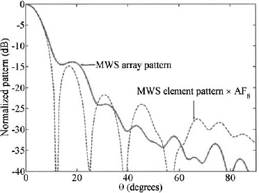
Figure 4.83. Plot of the polyrod element pattern, 8-element array factor, element pattern times array factor, and the 8-element array with mutual coupling.

Figure 4.84. Orthogonal cuts of the 4– × 8-element planar arrays of polyrod elements.
Figure 4.83 shows the far field of an 8-element array of the polyrod elements with d = 0.6λ. The dotted line is the array factor times the element pattern in Figure 4.82. The solid line is the array pattern of the 8-element array taking into account mutual coupling. Nulls and low sidelobes are not approximated well using the simple formula given by the element pattern times the array factor. Figure 4.84 compares the orthogonal antenna pattern cuts of 4-element and 8-element linear arrays of tapered polyrods (d = 0.6λ) when mutual coupling is included in the calculations. The arrays lie along the x axis, so the patterns at ![]() = 90° are nearly identical except that the 8-element array is about 3 dB higher, because it has twice the elements of the 4-element array.
= 90° are nearly identical except that the 8-element array is about 3 dB higher, because it has twice the elements of the 4-element array.
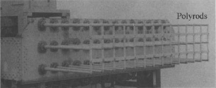
Figure 4.85. Mark 8 planar phased array with polyrod elements. (Courtesy of the National Electronics Museum.)
Bell Labs built the X-band surface fire control radar, the Mark 8 using an array of 42 polyrods, configured as a planar array having 14 × 3 elements as shown in Figure 4.85. This was the first use of the polyrod antenna in an array, and the first microwave phased array. Each column of three elements received the same phase shift. Rotary phase shifters adjusted the phase of each column of elements to steer the beam. The array had 2° azimuth and 6.5° elevation beamwidths [49].
REFERENCES
- P. Hannan, The element-gain paradox for a phased-array antenna, IEEE Trans. Antennas Propagat., Vol. 12, No. 4, 1964, pp. 423–433.
- D. Carter, Phase centers of microwave antennas, IRE Trans. Antennas Propagat., Vol. 4, No. 4, 1956, pp. 597–600.
- J. Huang, A technique for an array to generate circular polarization with linearly polarized elements, IEEE AP-S Trans., Vol. 34, No. 9, September 1986, pp. 1113–1124.
- R. C. Hansen, Phased Array Antennas, New York: John Wiley & Sons, 1998.
- D. N. McQuiddy, Jr., R. L. Gassner, P. Hull et al., Transmit/receive module technology for X-band active array radar, Proc. IEEE, Vol. 79, No. 3, 1991, pp. 308–341.
- R. T. Compton, On the performance of a polarization sensitive adaptive array, IEEE AP-S Trans., Vol AP-29, September 1981, pp. 718–725.
- R. L. Haupt, Adaptive crossed dipole antennas using a genetic algorithm, IEEE AP-S Trans., Vol. 52, No. 8, August 2004, pp. 1976–1982.
- http://www.haarp.alaska.edu/haarp/index.html
- R. E. Collin, Antennas and Radiowave Propagation, New York, McGraw-Hill, 1985.
- R. G. Fitzgerrell, Monopole impedance and gain measurements on finite ground planes, IEEE Trans. Antennas Propagat., Vol. 36, No. 3, 1988, pp. 431–439.
- R. L. Haupt and D. W. Aten, Low sidelobe arrays via dipole rotation, IEEE AP-S Trans., Vol. 57, No. 5, May 2009, pp. 1574–1577.
- J. D. Kraus and R. J. Marhefka, Antennas for All Applications, 3rd ed., New York: McGraw-Hill, 2002.
- W. L. Stutzman and G. A. Thiele, Antenna Theory and Design, 2nd ed., New York: John Wiley & Sons, 1998.
- H. King and J. Wong, Characteristics of 1 to 8 wavelength uniform helical antennas, IEEE Trans. Antennas Propagat., Vol. 28, No. 2, 1980, pp. 291–296.
- C. A. Balanis, Antenna Theory: Analysis and Design, 3rd ed., Hoboken, NJ: Wiley-Interscience, 2005.
- National RadioAstronomy Observatory, An overview of the very large array, http://www.vla.nrao.edu/genpub/overview/, June 17, 2009.
- R. S. Elliott, Antenna Theory and Design, revised edition, Hoboken, NJ: John Wiley & Sons, 2003.
- National Electronics Museum, RARF Antenna, 2009, Display Information.
- National Electronics Museum, EAR Antenna, 2009, Display Information.
- R. S. Elliott, Antenna Theory and Design, revised edition, Hoboken, NJ: John Wiley & Sons, 2003.
- A. J. Stevenson, Theory of slots in rectangular waveguides, J. Appl. Phys., Vol. 19, January 1948, pp. 24–38.
- A. Oliner, The impedance properties of narrow radiating slots in the broad face of rectangular waveguide: Part I—Theory, IRE Trans. Antennas Propagat., Vol. 5, No. 1, 1957, pp. 4–11.
- A. Oliner, The impedance propeties of narrow radiating slots in the broad face of rectangular waveguide: Part II—Comparison with measurement, IRE Trans. Antennas and Propagat., Vol. 5, No. 1, 1957, pp. 12–20.
- AN/APG-68(V) airborne fire-control radar, Jane’s Radar and Electronic Warfare Systems, 21-Dec-2007.
- A. J. Haupt, Antennas, IEEE Aerospace Junior Engineering Conference, March 2008.
- D. R. Jackson and N. G. Alexopoulos, Simple approximate formulas for input resistance, bandwidth, and efficiency of a resonant rectangular patch, IEEE Trans. Antennas Propagat., Vol. 39, No. 3, 1991, pp. 407–410.
- R. Garg, P. Bhartia, I. Bahl, and A. Ittipiboon, Microstrip Antenna Design Handbook, Norwood, MA: Artech House, 2001.
- M. Kara, Formulas for the computation of the physical properties of rectangular microstrip antenna elements with various substrate thicknesses, Microwave Opt. Technol. Lett., Vol. 12, No. 4, 1996, pp. 234–239.
- N. J. McEwan, R. A. Abd-Alhameed, E. M. Ibrahim et al., A new design of horizontally polarized and dual-polarized uniplanar conical beam antennas for HIPERLAN, IEEE Trans. Antennas Propagat., Vol. 51, No. 2, 2003, pp. 229–237.
- Z. N. Chen, Broadband Planar Antennas, Hoboken, NJ: John Wiley & Sons, 2006.
- J. Dyson, The equiangular spiral antenna, IRE Trans. Antennas Propagat., Vol. 7, No. 2, 1959, pp. 181–187.
- W. Curtis, Spiral antennas, IRE Trans. Antennas Propagat., Vol. 8, No. 3, 1960, pp. 298–306.
- M. Gustafsson, Broadband Self-Complementary Antenna Arrays, C. E. Baum, A. P. Stone, and J. S. Tyo, ed., Ultra-Wideband Short-Pulse Electromagnetics 8, New York, Springer, 2007.
- J. Kaiser, The Archimedean two-wire spiral antenna, IRE Trans. Antennas Propagat., Vol. 8, No. 3, 1960, pp. 312–323.
- M. Lee, B. A. Kramer, C. Chi-Chih et al., Distributed lumped loads and lossy Transmission Line Model for Wideband Spiral Antenna Miniaturization and Characterization, IEEE Trans. Antennas Propagat., Vol. 55, No. 10, 2007, pp. 2671–2678.
- J. Dyson, The unidirectional equiangular spiral antenna, IRE Trans. Antennas Propagat., Vol. 7, No. 4, 1959, pp. 329–334.
- R. Guinvarc’h and R. L. Haupt, Dual polarization interleaved spiral antenna phased array with an octave bandwidth, IEEE Trans. Antennas Propagat., Vol. 58, No. 2, 2010, pp. 1–7.
- B. Alien, Ultra-Wideband: Antennas and Propagation for Communications, Radar and Imaging, Chichester: John Wiley & Sons, 2007.
- G. H. Brown and J. O. M. Woodward, Experimentally determined radiation characteristics of conical and triangular antennas, RCA Rev., Vol. 13, No. 4, December 1952, pp. 425–452.
- Z. N. Chen, Broadband Planar Antennas, Hoboken, NJ: John Wiley & Sons, 2006.
- P. J. Gibson, The Vivaldi aerial, 9th European Microwave Conference Proceedings, 1979, pp. 103–105.
- W. E Croswell, T. Durham, M. Jones, D. Schaubert, P. Friederich, and J. G. Maloney, Wideband arrays, in Modern Antenna Handbook, C. A. Balanis, ed., Hoboken, NJ: John Wiley & Sons, 2008, pp. 581–630.
- J. S. Mandeep and Nicholas, Design an X band Vivaldi antenna, Microwaves & RF, July 2008, pp. 59–65.
- H. Oraizi and S. Jam, Optimum design of tapered slot antenna profile, IEEE AP-S Trans., Vol. 51, No. 8, 2003, pp. 1987–1995.
- T. H. Chio and D. H. Schaubert, Parameter study and design of wide-band widescan dual-polarized tapered slot antenna arrays, IEEE Trans. Antennas Propagat., Vol. 48, No. 6, 2000, pp. 879–886.
- H. Holter, C. Tan-Huat, and D. H. Schaubert, Elimination of impedance anomalies in single- and dual-polarized endfire tapered slot phased arrays, IEEE Trans. Antennas Propagat., Vol. 48, No. 1, 2000, pp. 122–124.
- H. Holter, C. Tan-Huat, and D. H. Schaubert, Experimental results of 144-element dual-polarized endfire tapered-slot phased arrays, IEEE Trans. Antennas Propagat., Vol. 48, No. 11, 2000, pp. 1707–1718.
- R. Horner, B. Calder, R. Mangra et al., Tapered slot antenna cylindrical array, US7518565, April 14,2009.
- L. Brown, A Radar History of World War II: Technical and Military Imperatives, Philadelphia: Institute of Physics Publishing, 1999.