
4
Capacitive sensors for displacement measurement in the subnanometer range
Abstract
The main challenge in designing an interface circuit for capacitive displacement sensors with subnanometer resolution is the large offset capacitance of the sensor. This offset capacitance results from the relatively large distance between the sensor electrodes, compared with the displacement range to be measured. Of the different methods, which interface capacitive sensors, a charge-balancing technique is used here to demonstrate a power-efficient way to remove the offset, while maintaining high resolution and a short conversion time. To demonstrate this technique, the design of an oversampling capacitance-to-digital converter based on a third-order sigma/delta modulator is presented.
Keywords
Capacitance-to-digital converter; Capacitive displacement sensor interface; Incremental ΣΔ converter; Offset capacitance cancellation; Switched-capacitor circuits
4.1. Introduction
Capacitive sensors are widely used to measure a variety of physical quantities, such as pressure, position, proximity, and humidity (Omran et al., 2014a,b; Omran et al., 2017; Boser, 2012; Tan et al., 2011, 2013; Xia et al., 2012; Ha et al., 2014; Yang and Nihtianov, 2013; Oh et al., 2015; Sanjurjo and Prefasi, 2015; Sanjurjo et al., 2016; He et al., 2015). One reason for the widespread application of capacitive sensors is that the sensor itself consumes no static power, making it very suitable for low power applications. However, to make the complete capacitance measurement system low power, the power consumption of the electronic readout circuit also needs to be kept low, which is the real challenge.
Over the years, a wide variety of architectures have been reported in the literature for capacitance-to-digital converter (CDC) design, including successive-approximation-register (SAR) (Omran et al., 2014a, 2017), sigma–delta (ƩΔ) (Boser, 2012; Tan et al., 2011, 2013; Xia et al., 2012; Ha et al., 2014; Yang and Nihtianov, 2013), dual slope (Oh et al., 2015; Omran et al., 2014b; Sanjurjo and Prefasi, 2015; Sanjurjo et al., 2016), period/pulse-width modulation (He et al., 2015), and hybrid (Sanyal and Sun, 2016). Many interesting hybrid topologies have been explored, which push the energy efficiency of the CDC to a higher level. As the various capacitance-to-digital conversion principles have different properties, some may be more suitable than other types of topologies depending on the sensing specifications. For example, the SAR topology can be suitable for low-to medium-resolution CDCs and can achieve an impressive energy efficiency figure-of-merit (FoM) (Omran et al., 2017), whereas CDCs based on the ƩΔ topology can achieve high resolution that is otherwise difficult to achieve with other topologies (Boser, 2012). However, the downside of CDCs based on the ƩΔ topology is that they often have relatively low energy efficiency. One of the fundamental reasons for this is that the ƩΔ CDC requires a large oversampling ratio (OSR) to achieve high resolution. The zoom-in architecture, on the other hand, reduces the OSR required for a certain resolution by reducing the conversion range of the CDC (Souri et al., 2012; Chae et al., 2013).
Although it makes sense to compare the energy efficiency FoM of different CDCs as an indication of their relative performance, it should be pointed out that the amount of baseline capacitance relative to the sensor capacitance variation adds to the complexity of the problem. This is because for a fixed sensor capacitance variation range, the larger the baseline capacitance, the higher the noise (O'Dowd et al., 2005), and hence the lower the resolution and the worse the FoM. Therefore, when comparing the energy efficiency of a CDC this should also be considered.
Large offset capacitance often presents problems in capacitive sensor measurements. In this chapter, we discuss a capacitive sensor interface circuit based on the charge-balancing technique, which removes the effect of offset capacitance electrically. High resolution is achieved within a relatively short conversion time.
4.2. Challenges for subnanometer displacement measurement with capacitive sensors
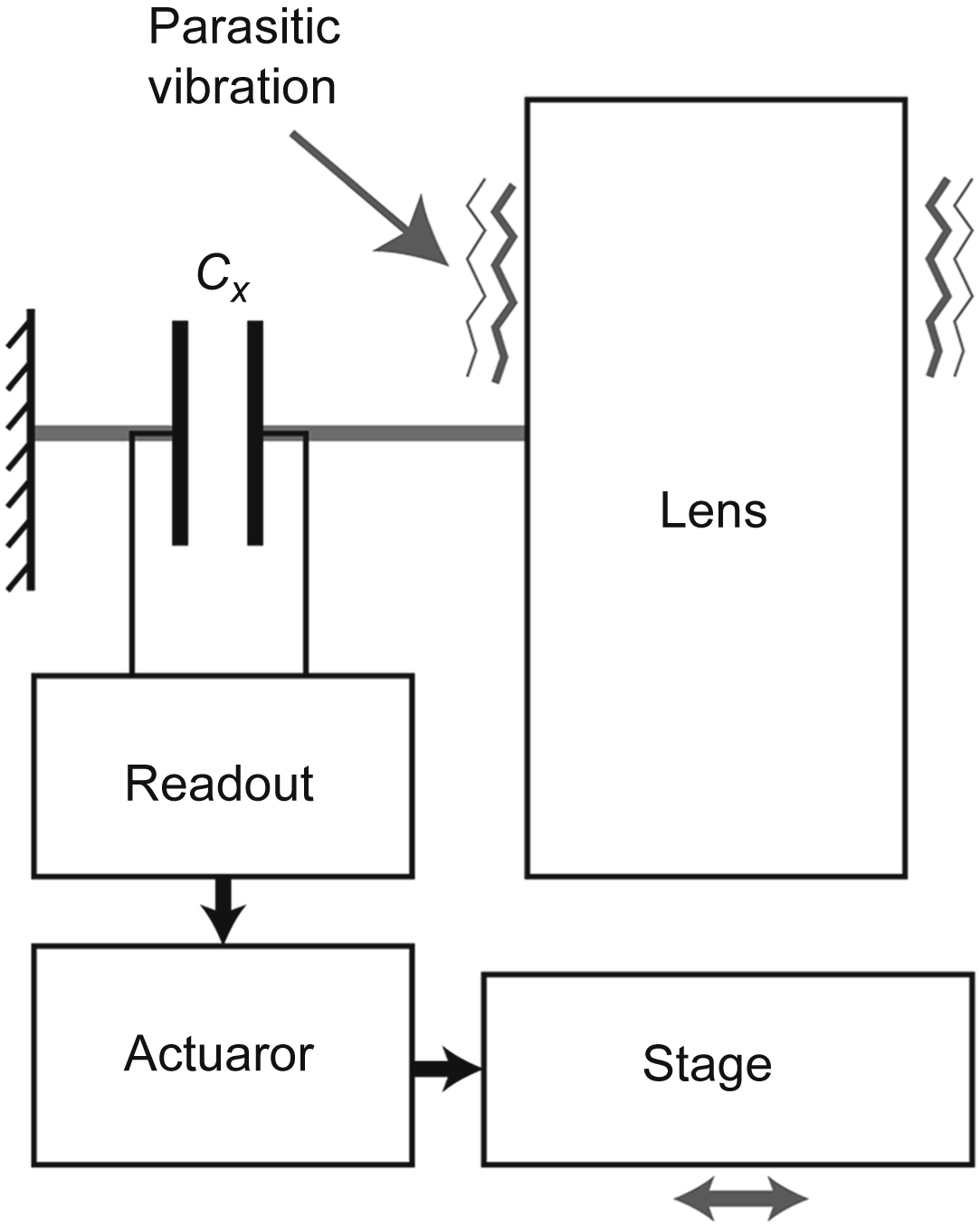
In precision mechatronic systems such as wafer steppers, electron microscopes, etc., the position of critical mechanical components must be dynamically stabilized with subnanometer precision. This can be achieved with a servo loop consisting of a displacement sensor and an actuator, which performs a vibration-dumping function that synchronizes the vibration of one part of a system (lens column) with the movement of another part (stage), as shown in Fig. 4.1. For this application, capacitive displacement sensors offer a smaller component size and lower cost, compared with other sensors, such as optical interferometers. Another important advantage of capacitive sensors is that they neither consume nor generate electrical energy when converting displacement into an electrical signal and, hence, they produce no electronic noise, which is a prerequisite for obtaining extremely high resolution.
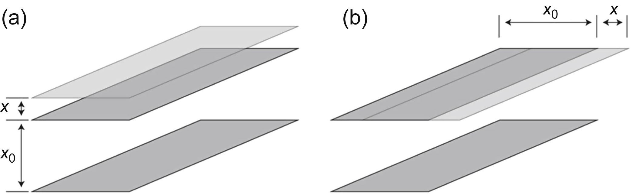
In Fig. 4.2, a parallel plate capacitive sensor is shown, the capacitance of which is a function of the gap and overlap between the two plates. The changes in both of the physical parameters can be used to sense displacement. In both cases, the sensitivity to a small displacement x is Boser (2012):
where C0 is the nominal capacitance at x0, and x0 is the gap between the plates or the width of the overlap between the plate. It can be seen that decreasing x0 can increase the sensitivity of the capacitive sensor. For typical geometries, the gap is much smaller than the overlap; thus, for high-sensitivity capacitive displacement sensors, the variation in the plate gap is generally used. However, higher sensitivity comes at the cost of nonlinearity because, for the gap-closing transducer, the capacitance change is a known nonlinear function of displacement. Nevertheless, if x0 is known, this nonlinearity can be accounted for by back-end processing.
From the above discussion, it is clear that for maximum sensitivity, the gap between the plates should be as small as possible. However, mechanical tolerances limit the minimum gap width between the sensor electrodes to a few micrometers (van Schieveen et al., 2010), whereas in the targeted applications the required resolution must be in the subnanometer range (typically, below 100 p.m.). At the same time, the displacement and/or vibrations of the target to be measured are normally less than 1 μm. In terms of capacitance values, if the nominal sensor capacitance at x0 = 10 μm is 10 pF, the interface circuit needs to have an input-referred capacitance resolution of better than 100 aF. As a comparison, the variation in the sensor capacitance relative to the displacement range will be much less than 1 pF because of the low sensitivity of the capacitive sensor to displacement. Thus, the sensitivity of the displacement sensor becomes limited by the attainable gap distance. This also means that the readout circuit needs to have greater than 17-bit resolution with respect to the nominal sensor capacitance. Furthermore, in servo-loop applications, often the measurement latency needs to be very low. The main challenge for the electronic interface is to provide high-resolution capacitance measurement with low measurement latency, which is challenging because of the trade-off between measurement time and resolution.
Because the nominal capacitance of the sensor is much larger than the variation in sensor capacitance, it can be assumed that the sensor has a large offset capacitance. Luckily, there are ways to deal with this, as will be discussed in the next section.
4.3. Offset capacitance cancellation technique
The existence of offset capacitance in a capacitive sensor often imposes a burden on the interface circuit. As the value of the sensor capacitance is dominated by the offset value, the interface circuit must resolve the relatively small capacitance variation on top of the offset capacitance. Offset capacitance consumes a large portion of the dynamic range of the interface, which translates into a waste of system resources, such as power consumption and conversion time.
Fortunately, there are techniques to create circuits that cancel the effects of the offset capacitance (AD7746 Datasheet; Shin et al., 2011). Typically, a capacitive sensor interface involves a virtual ground created by an operational amplifier to render the readout of the capacitive sensor interface insensitive to parasitic capacitances to ground at each of the two connections (O'Dowd et al., 2005; Baxter, 1996). Such a virtual ground can also be used to cancel the effect of the offset capacitance because a “zoom-in” capacitor can be connected to the virtual ground and then driven by an excitation signal that is opposite to that driving the sensor capacitor. The net charge that travels through the virtual ground and arrives at the feedback capacitor is then a function of the difference between the sensor capacitor and the zoom-in capacitor. By establishing the value of the zoom-in capacitor as being equal to the offset capacitance of the sensor, the effect of the large sensor offset capacitance can be eliminated.
However, it should be noted that this function comes at a price. With the addition of the zoom-in capacitor, the total capacitance at the input of the amplifier increases, which increases the noise gain of the amplifier (O'Dowd et al., 2005). The significance of this noise penalty depends on the component values. For instance, if the value of the parasitic capacitance at the input of the amplifier (e.g., due to a long cable) is much greater than the sensor capacitance (and, hence, the zoom-in capacitance), then the penalty of introducing this zoom-in capacitance is negligible. In most cases, the benefit of using the zoom-in capacitance overrides the penalty introduced. However, it is still worthwhile to keep this potential disadvantage in mind.
One way to measure capacitance is to compare it with a reference capacitance, by creating a ratio between the two. Although there are many ways to obtain the capacitance ratio, the most popular method for obtaining a high-resolution capacitive ratio is by using switched-capacitor circuitry combined with the charge-balancing principle (Schreier et al., 2005). This particular method has a proven track record of achieving both high resolution and high accuracy, at the expense of a generally slower conversion speed because it basically trades resolution for time (Wang et al., 1998). Fig. 4.3(a) shows a block diagram of a capacitive sensor based on the charge-balancing principle. It is basically a switched-capacitor incremental ΣΔ converter (Norsworthy et al., 1997). In such a system, a virtual ground is also available to realize offset capacitance cancellation, as shown in Fig. 4.3(b).
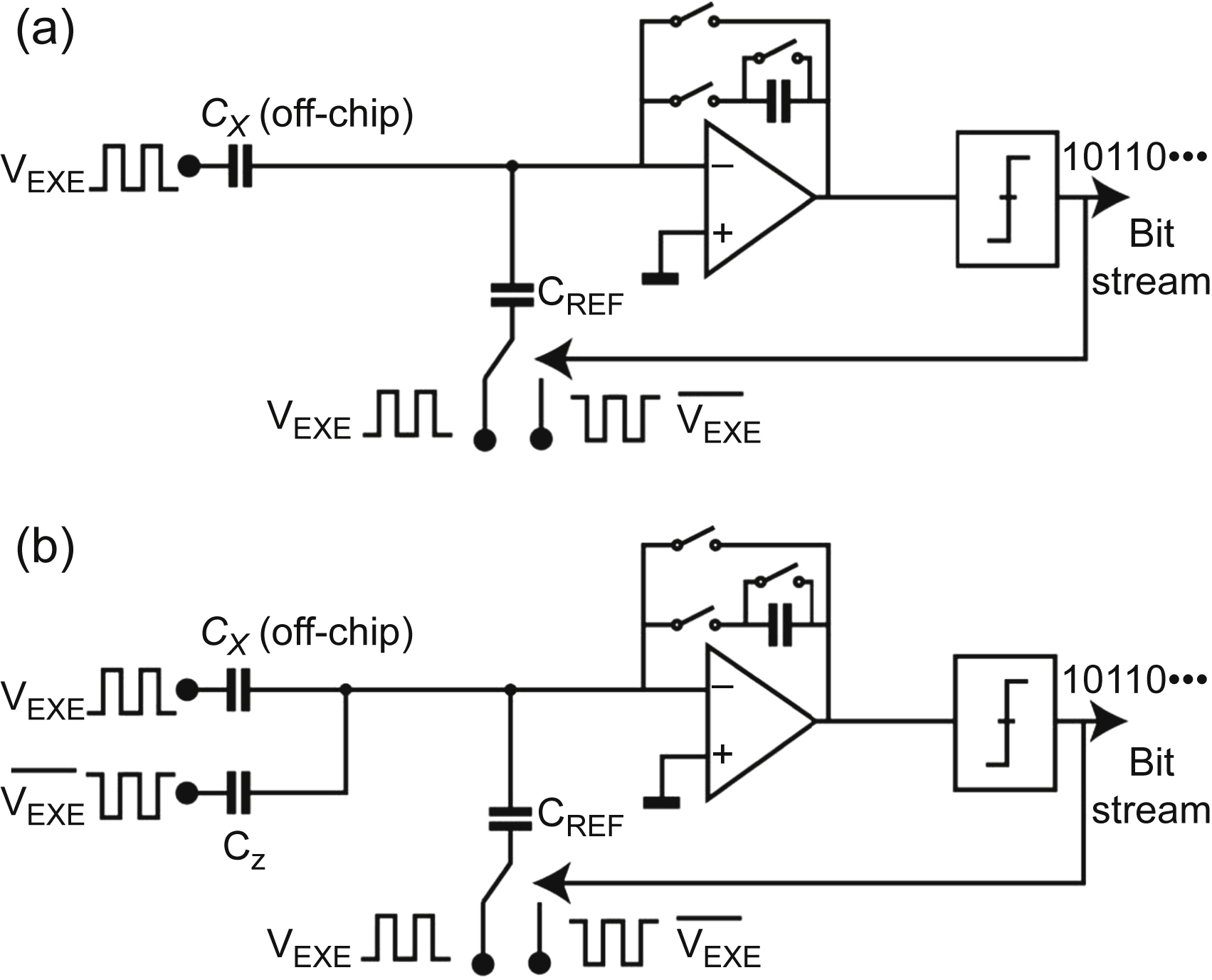
One of the most important advantages of switched-capacitor circuits in terms of realization is the relaxed requirement for excitation signals. Mismatches in the excitation signals would normally translate into a perceived capacitance difference that would lead to an error in the readout circuit. For a switched-capacitor circuit, however, because the circuit is only sensitive to the final settled voltage values, the exact waveform of the two antiphase excitation signals does not need to match perfectly, as long as there is no charge loss and there is no signal-picking at the input of the convertor. This simplifies the design a great deal.
The effective input of the interface becomes the difference between CX and CZ, i.e., CX–CZ. When the value of CZ is selected such that it equals the offset capacitance of CX, the effect of the offset capacitance is completely eliminated. Then, a much lower Cref can be applied, which provides a measurement range that is just broad enough to cover the small capacitance variation ± ΔCX. In this way, the quantization requirement of the interface can be largely reduced. However, in practice it is difficult to ensure that CZ fully cancels the offset capacitance of CX, so some tolerances need to be considered when designing the interface. In the next section, a design example will be presented based on the method discussed above.
4.4. Capacitance-to-digital converter with offset capacitance cancellation and calibration functions
In this section, a design example is presented, which shows the benefits of using the zoom-in technique. With this technique, the switched-capacitor incremental converter digitizes the capacitive ratio. The performance of the interface before and after using the zoom-in technique will be compared.
In this design example, the specifications are taken from a real application. The capacitive displacement sensor has a nominal capacitance of 10 pF. The measurement range, in contrast, is less than 50 fF. The targeted resolution is greater than 100 aF. The noise of the interface can be classified into thermal noise and quantization noise, as other noise source such as 1/f noise can be removed relatively easily. (Schreier et al., 2005; O'Dowd et al., 2005) provide an extensive overview on this topic. The total noise power is the sum of the thermal noise power and the quantization noise power.
Thermal noise in a switched-capacitor circuit is directly linked to the size of the sampling capacitor (O'Dowd et al., 2005). For an incremental converter, which utilizes the oversampling technique, thermal noise can be further reduced by increasing the OSR. For a fixed conversion time, both methods for reducing thermal noise would require the interface to consume more power, either by driving larger capacitors or by using a faster clock. For a capacitive sensor interface circuit based on an incremental converter, the sensing capacitor acts as a sampling capacitor (O'Dowd et al., 2005), the value of which is often fixed and cannot be changed arbitrarily by the designer. Therefore, the only way to reduce thermal noise in such an interface is by increasing the OSR.
Consequently, increasing the OSR also reduces the quantization noise level (Wang et al., 1998). Depending on the loop filter structure, the slope at which the quantization noise is reduced will also change. Generally speaking, the higher the order of the loop filter, the faster the quantization noise reduces with the increasing OSR. Apart from using higher-order loop filters, a multibit quantizer can be used, instead of a single-bit quantizer, to increase the speed of operation. Because of the noise-shaping effect on the quantization noise, the quantization noise decreases more rapidly than the thermal noise as the OSR is increased.
As discussed in the previous section, the zoom-in technique does not help to reduce the thermal noise level. Therefore, basically, the thermal noise of the interface is determined to some extent by the absolute value of the sensor capacitor, which in our case is about 10 pF. Zoom-in, however, reduces the full-scale input range of the interface and therefore reduces the requirement on the quantization noise of the interface. As a result, it is important to point out that using the zoom-in technique only makes sense if, before it is applied, the quantization noise level is greater than the thermal noise level. In this example, the estimation of the thermal noise level is performed under the guidance provided by Schreier et al. (O'Dowd et al., 2005). This work shows that an OSR of about 100 is needed to reduce the input-referred thermal noise level to a sufficiently low level. Thus, to prevent the quantization noise from limiting the interface resolution, we need to achieve a comparably low quantization noise level within an OSR of 100.
Without employing the zoom-in technique, the input signal range, including the offset capacitance, would be about 10 pF. Achieving a capacitance resolution below 100 aF would require more than a 17-bit dynamic range. Therefore, the questions here are how much resolution can be achieved with an OSR of 100, and will the corresponding input range be sufficiently large to cover the sensor capacitance variation during normal operation?
Although a multibit quantizer and a digital-to-analog converter (DAC) can be used to reduce the required OSR, one of the most pronounced problems with this method is that the nonlinearity of the required multibit DAC limits the linearity of the modulator. This is because the DAC is in the feedback and its error is directly added to the error of the modulator. To solve this problem, dynamic element matching must be used (Wang et al., 1998). However, the consequence is hardware complexity. Because a 1-bit DAC is intrinsically linear, it does not suffer from this problem. Therefore, to reduce hardware complexity, a higher-order loop filter is mainly chosen as the optimum approach.
The sigma–delta modulator theory, which is based on a linearized model, can predict the necessary OSR for a particular resolution, with a certain loop filter order. However, at low OSR values, the prediction is often not very accurate, especially for incremental converters. A dedicated model was made, which led to complicated results for the prediction of the required OSR for an incremental converter (Markus et al., 2004). The authors therefore recommend using these results as guidelines only and relying on a system-level simulation to obtain a better estimation. The conclusion based on the simulations results is that, with an OSR in the order of 100:
- 1. a second-order loop filter will not meet the requirement of an input capacitance range of 50 fF, which is not acceptable for this application;
- 2. increasing the loop filter beyond third order brings negligible improvement. For this reason, a third-order loop filter has been chosen for this design.
With a third-order loop filter, the input range is selected to be 200 fF, which ensures sufficient margin to cover the variation in the sensor capacitance, while also providing some margin for the mismatch between the sensor capacitance CX and the offset-canceling capacitance CZ. This means that the resolution must be greater than 12 bits when the zoom-in technique is applied.
With a third-order loop filter, a very good quality decimation filter must be used in the CDC to reach the required capacitance resolution within the limited conversion time. Fig. 4.4 shows the attainable resolution of three different decimation filters for a ΣΔ converter with a third-order loop filter, as a function of the number of clock cycles in one conversion, using the formulas given in Markus et al. (2004). It can be seen that only a cascade of integrators (CoI) decimation filter can reach greater than 12-bit resolution within 100 clock cycles. Conventional sinc3 and sinc4 filters need 240 and 160 clock cycles, respectively, to reach the same resolution. To maintain a short conversion time, a higher clock signal is needed. For example, for a conversion time below 20 μs and 100 clock cycles, a 5 MHz clock signal is required.
In comparison, if the zoom-in technique is not applied, the same third-order incremental converter would need an OSR larger than 500 to reach a quantization noise level equivalent to 17 bits. Therefore, in this example, by applying zoom-in, the conversion time with the same clock frequency will be 5 times shorter. In addition, as will be discussed below, using the zoom-in principle also prevents slewing in the amplifier. This property can be further utilized to increase the clock frequency of the converter with the same amount of current consumed by the amplifiers. In this sense, the actual benefit of applying the zoom-in principle is greater than 5 times.
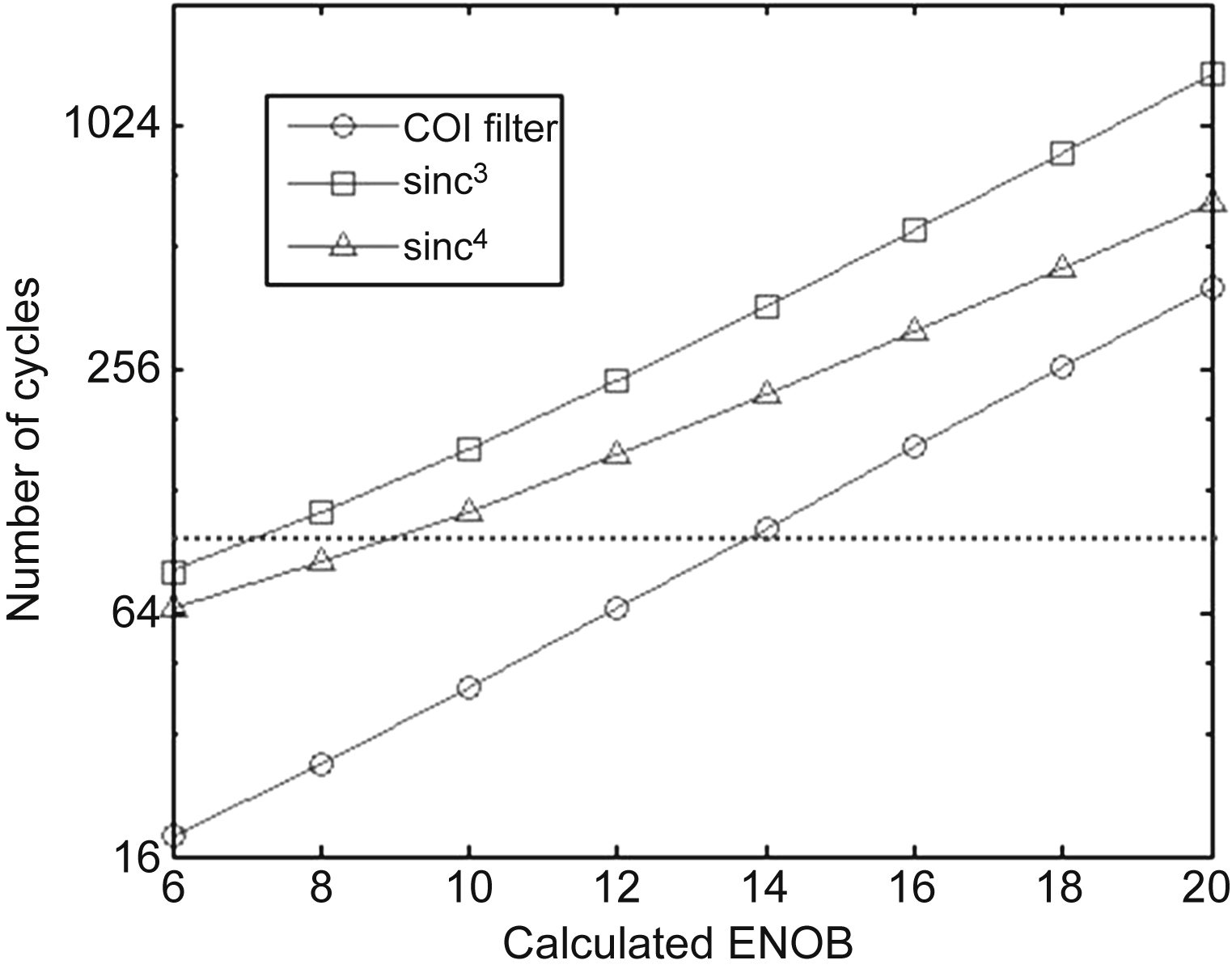
Figure 4.4 Achievable resolution of three different decimation filters for a ΣΔ converter with a third-order loop filter as a function of the number of clock cycles. COI, cascade of integrators; ENOB, effective number of bits.
To prove the validity of the above discussions, a capacitive sensor interface has been realized, a block diagram of which is presented in Fig. 4.5. The interface is built around the switched-capacitor sigma–delta converter shown in Fig. 4.6 (Tan et al., 2013). The zoom-in capacitor CZ is realized with a bank of on-chip capacitances CapDAC (i.e., a capacitive digital-to-analog converter) to be able to easily adjust the value to match that of the sensor capacitance. The CapDAC is basically a binary bank of capacitors that can switch in and out by applying a digital code. The interface is fabricated in a standard 2P4M 0.35 μm complementary metal–oxide semiconductor process and occupies an active area of 2.6 × 2 mm. A microphotograph of the chip layout is shown in Fig. 4.7. It draws 4.5 mA from a 3.3 V supply, of which over 3.1 mA is consumed by the first operational transconductance amplifier to drive large capacitances. The CapDAC and all the other on-chip capacitors are poly–poly capacitors because of their good linearity and temperature stability. For flexibility, in this design the control logic and the decimation filter are implemented off-chip.
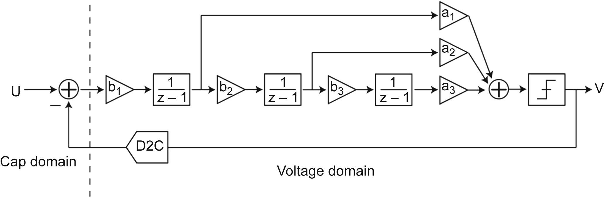

Figure 4.6 Simplified circuit diagram of the interface showing different timing diagrams in different operating modes. CapDAC, capacitive digital-to-analog converter.
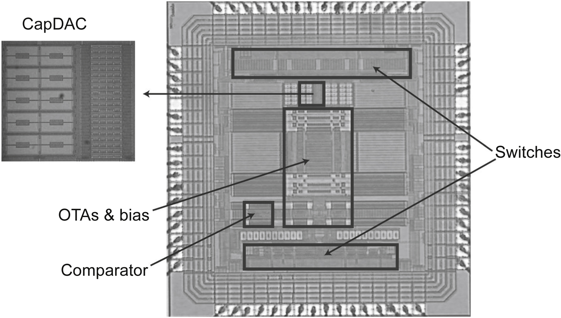
Figure 4.7 Die micrograph. CapDAC, capacitive digital-to-analog converter; OTA, operational transconductance amplifier.
To verify the performance of the CDC with an off-chip sensor, a test setup was built. As shown in Fig. 4.8, it consists of a fixed electrode in close proximity to an electrode attached to an aluminum rod. Heating the rod, via an attached resistor, changes its length and thus the capacitance between the two electrodes. The CDC is connected to the electrode on the rod via a short shielded cable, which adds extra parasitic capacitance (roughly 10 pF) to ground. The small capacitance changes created by driving the heater with a 66 mHz, 8 mW square wave are shown in Fig. 4.9. Because of the inertia of the thermal excitation, the range of motion decreases steeply as the driving frequency increases. To obtain an observable displacement with reasonable power consumption, the driving signal frequency is limited to 66 mHz. The actual value of the reference capacitor Cref, as shown in Fig. 4.6, was found to be 91.8 fF by calibrating it against an external 10.3 pF surface-mount capacitor the value of which had been measured by a HP4192A LF impedance analyzer (±100 fF inaccuracy). The capacitance changes were then found to correspond to 500 aF (pick-to-pick), according to Fig. 4.9, whereas the noise on the measurements corresponded to 65 aF (rms).


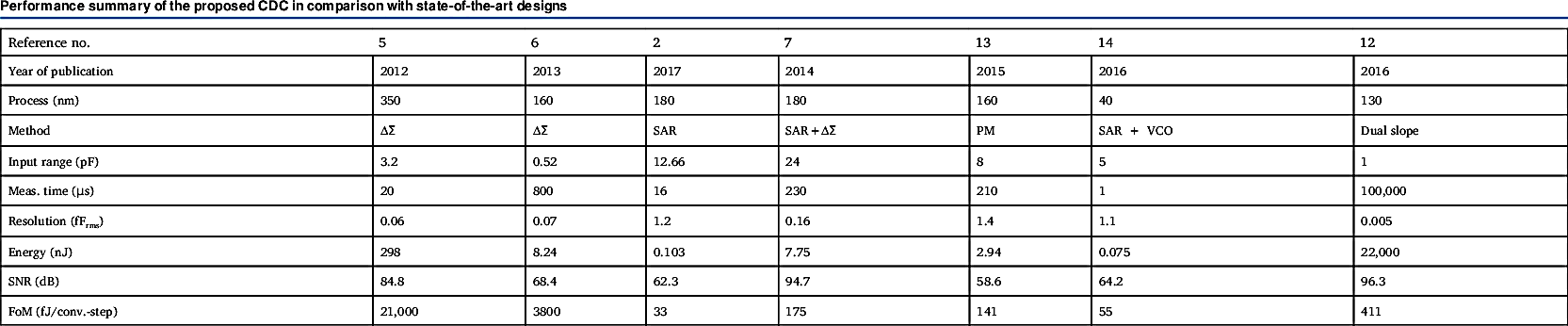
In recent years, offset capacitance cancellation has been applied to various other capacitive interface designs, leading to applications in fields such as humidity sensors. Moreover, in the race to push the energy efficiency of capacitive sensor interface circuits, the zoom-in principle continues to dominate high-resolution high-accuracy capacitive sensor interfaces. Table 4.1 lists the performance of state-of-the-art CDCs reported in recent years. Note that the specifications of the different circuits vary by a considerable amount, which is due to the enormous differences in areas of application. Although much better FoMs have been achieved with architectures such as SAR and Voltage-Controlled Oscillator-based capacitive sensor interfaces (Omran et al., 2017; Sanjurjo et al., 2016; He et al., 2015; Sanyal and Sun, 2016), their resolution remains at sub–10-bit levels, limiting their applicability to less demanding tasks. On the other hand, architectures based on zoom-in have achieved a respectable FoM while also achieving resolution exceeding 15 bits (Xia et al., 2012; Tan et al., 2013; Ha et al., 2014).
Table 4.1
4.5. Conclusion
A practical method for removing the effect of offset capacitance in a capacitive sensor has been presented. The interface circuit design makes use of the charge-balancing principle and achieves an effective capacitance resolution of 17 bits within a conversion time of 20 μs (5 Mhz clock frequency, 100 times oversampling).
..................Content has been hidden....................
You can't read the all page of ebook, please click here login for view all page.