
Chapter 2
Introduction to Digital Circuits
2.1 Basics of Modern Digital Circuits
Since the invention of complementary metal-oxide-semiconductor (CMOS) technology, digital logic circuits have contributed to processing massive digital data. Examples of the applications based on the digital processing are laptop computers, smart phones, wearable devices, smart cards, and so on. In this chapter, we learn the basics of how to implement a digital hardware. Especially, synchronous design, which is commonly applied to most of the digital circuits, is introduced as a key technology.
The synchronous design uses a clock signal that is distributed to the whole synchronous circuits, and takes the timing of operations. To look into the details of the synchronization mechanism, the building blocks in the synchronous circuit are described. As they play an important role in the digital circuits, memory modules are also discussed.
2.1.1 Digital Circuit Design Method
Many modern digital circuits are implemented based on the synchronous design method that can handle integrated circuits (ICs) by using commercial design automation (DA) tools. As illustrated in Figure 2.1, the synchronous design starts from register transfer level (RTL) coding after defining a design specification. At this design stage, the designers can know the speed performance and the design validity by RTL simulators. Different from a normal program code of C language, an RTL code has information of timing that determines when each variable is changed or how long it should keep the same value.

Figure 2.1 An overview of synchronous-style design flow
The RTL simulation speed is fast enough to perform a lot of functional tests of the code. Therefore, the debugging and performance test of the design should be done at this stage, and the simulation results are fed back to the design specification, if necessary. Note that design synthesis to a gate-level description is necessary to estimate the area cost.
2.1.2 Synchronous-Style Design Flow
Synchronous-style design method is one of the design methods that have led the evolution of digital circuits since around 1990s. Compared to the asynchronous-style design flow, where the data processing timing is not triggered by the clock edge, the synchronous-style one has advantage in that there is a design flow where many design steps are automated by DA tools. An overview of the design flow is shown in Figure 2.1.
- Specification: Designers define the specification of digital circuits. The specification describes the interface and its characteristics, necessary functionality, speed performance, and so on.
- RTL coding: Designers can use a high-abstraction-level language as an entry of implementation of the digital circuit such as Verilog HDL (hardware description language) or Verilog for short, which directly contributes to a high productivity in the design flow.1
- Logic synthesis: An RTL description programmed with Verilog is automatically synthesized to gate-level description that is called netlist.
- Layout: Logical gates and wires in the synthesized design are allocated physically by using a layout tool automatically.
Cryptographic hardware, which is the target device in this book, can be seen as one of the digital circuits, and hence the synchronous-style design flow or similar one is often used.
2.1.3 Hierarchy in Digital Circuit Design
Digital circuits have many functional blocks such as controller, datapath including arithmetic logic unit, memory, and so on. Therefore, hierarchical structure is introduced in designing the digital circuit in order to divide the functionality and to ease the design verification.
Figure 2.2 illustrates the hierarchical structure in a modern digital circuit. Each node in the hierarchical directory tree is called a module that is a unit of functional block. The top module usually contains several submodules, and a multiple nest structure is constructed. An example of the structure of modules is shown in Figure 2.2.

Figure 2.2 Hierarchical structure in digital circuit design
In this case, the top module has three submodules, one of which, module C, has a submodule, module D. Modules B1 and B2 have the same functionality when they are instantiated from the same module. Each module has input, output, and inout ports that are connected to ports of other modules. Modules B1 and B2 contain sequential logics that will be explained in Section 2.3.2, and hence the clock and reset signals are provided as input.
2.2 Classification of Signals in Digital Circuits
Before discussing the details of designing digital hardware, classification of signals, propagating through wires and modules, is explained here. There are three main types of signals; clock, reset, and data signals. Note that clock and reset signals are not described in an algorithm-level description, where only data flow is used. On the other hand, clock and reset signals play an important role in a synchronous-style hardware design.
2.2.1 Clock Signal
The clock signal requires a special consideration concerning the routing of its signal line so that all circuits can start operation at the same timing. More precisely, it is necessary that all the sequential logic gates, which will be explained later, using the clock signal have to detect the positive edge (or negative edge) of the clock at the same or quite similar timings.
However, even if the wiring delay of the clock signal is routed carefully, there exists a slight difference in the arrival time of the sequential logics. Such timing difference is called clock skew, and its maximum difference is denoted as ![]() as illustrated in Figure 2.3. Moreover, there exists another clock timing difference called clock jitter, which also effects the timing difference. It is a distortion of the signal caused when it is generated in a clock generator and is distributed to the circuit. In this chapter, it is assumed that the clock jitter is appropriately controlled for simplicity.
as illustrated in Figure 2.3. Moreover, there exists another clock timing difference called clock jitter, which also effects the timing difference. It is a distortion of the signal caused when it is generated in a clock generator and is distributed to the circuit. In this chapter, it is assumed that the clock jitter is appropriately controlled for simplicity.

Figure 2.3 Image of clock skew
The simplest way to realize the synchronous-style circuit is to use a single clock with a clock frequency, ![]() . The clock period,
. The clock period, ![]() , is the inversion of the clock frequency. That is,
, is the inversion of the clock frequency. That is,
Although the timing management becomes complex, it is also possible to employ multiple clocks with different clock frequencies.
2.2.2 Reset Signal
Reset signal is also a special signal used for initializing the value of logics. When powering on a synchronous hardware, the initial state of the sequential logics (details in Section 2.3.2) is not always the expected initial values. In order to make the same initial state after powering on, a power-on reset is normally performed. In addition, the reset can interrupt an operation while it is running, and can initialize the state at any time.
In a synchronous design, synchronous or asynchronous reset can be used. The synchronous reset initializes the sequential logics when the active reset signal is detected when the positive edge of the clock signal arrives. On the other hand, the asynchronous reset can initialize the sequential logics regardless of the clock timing. Therefore, it can reset the sequential logics even when the clock signal is not provided, for example, immediately after powering on the circuit.
Both the resets have merits and demerits depending on the available library of sequential logics and design rule for the reset signal. The asynchronous reset is used for the sequential logics in this chapter, considering that further discussion can be continued without loss of generality. However, the deactivate timing of the reset should be handled with care in relation to the clock signal timing as the release timing of the reset needs to be the same for all the sequential logics. Namely, the arrival timings of the asynchronous reset signals vary depending on the sequential circuit position, and moreover there exist the clock skew and clock jitter. One possible way for an appropriate reset is adjusting the deactivation timing of the reset with the clock signals (i.e., synchronously releasing the reset), whereas the activation timing keeps asynchronous with the clock signals (i.e., asynchronously starting the reset).
2.2.3 Data Signal
In the context of the synchronous-style design, data signals are regarded as signals that change at the positive edge of the clock. In simple terms, all the signals other than the clock and reset signals are considered as data signal. Except several special cases,2 input and output of the sequential logics are connected to the data signals, and combinatorial logics, which will be explained later, are composed of data signals.
2.3 Basics of Digital Logics and Functional Modules
2.3.1 Combinatorial Logics
Combinatorial logics have input and output data signals, and the output signals are determined after evaluating the input signals. For instance, one-bit full adder (FA) operates the bit-wise operations as
where s is the bit-wise sum, a and b the operands, and ![]() and
and ![]() the carry-in and carry-out signals, respectively. The FA module and its corresponding combinatorial logics are illustrated in Figure 2.4.
the carry-in and carry-out signals, respectively. The FA module and its corresponding combinatorial logics are illustrated in Figure 2.4.

Figure 2.4 One-bit full adder module and its corresponding combinatorial logics
As shown in Figure 2.5, connecting eight FAs, 8-bit ripple-carry adder is implemented.3 The pseudo Verilog code is described in Figure 2.6.

Figure 2.5 8-bit ripple-carry adder based on FAs
Suppose that the input signals are changed from all zeros to all ones at the same time, that is, both A and B are changed from 0 to F. The least significant bit (LSB) of the addition result, ![]() , is calculated as
, is calculated as ![]() after the three-input XOR operation by Equation (2.2), and the carry-out signal,
after the three-input XOR operation by Equation (2.2), and the carry-out signal, ![]() changes from
changes from ![]() to
to ![]() by Equation (2.3). Then,
by Equation (2.3). Then, ![]() and
and ![]() are determined based on the signal change of
are determined based on the signal change of ![]() . In this way, the addition results are determined bit by bit from LSB to most significant bit (MSB). That is, all the output signals are determined after the input signals are changed.
. In this way, the addition results are determined bit by bit from LSB to most significant bit (MSB). That is, all the output signals are determined after the input signals are changed.
Note that the calculation time of the combinatorial logic, which can be measured as the difference between the input and the output determination times, varies from the input differences in value. It is called path delay. Intuitively, a smaller difference in the input signals tends to result in a less path delay.4 However, this is not always true.
module 8bit_adder (A, B, S, Co);
input [7:0] A, B;
output [7:0] S;
output Co;
wire cout0, cout1,  ,cout7;
wire s0, s1,
,cout7;
wire s0, s1,  , s7;
full_adder FA0(A[0], B[0], 1'b0, s0, cout0);
full_adder FA1(A[1], B[1], cout0, s1, cout1);
, s7;
full_adder FA0(A[0], B[0], 1'b0, s0, cout0);
full_adder FA1(A[1], B[1], cout0, s1, cout1);
 full_adder FA7(A[7], B[7], cout6, s7, cout7);
assign S = {s7, s6,
full_adder FA7(A[7], B[7], cout6, s7, cout7);
assign S = {s7, s6,  , s0};
assign Co = cout7;
endmodule
module full_adder (a, b, cin, s, cout);
input a, b, cin;
output s, cout;
assign s = a | b | cin;
assign cout = (a & b) | (b & cin) | (cin & a)
endmodule
, s0};
assign Co = cout7;
endmodule
module full_adder (a, b, cin, s, cout);
input a, b, cin;
output s, cout;
assign s = a | b | cin;
assign cout = (a & b) | (b & cin) | (cin & a)
endmoduleFigure 2.6 Pseudo Verilog code for 8-bit ripple-carry adder
2.3.2 Sequential Logics
In contrast with combinatorial logics, the output of sequential logics is determined with its current value and the input signals. Figure 2.7 shows the schematics and of positive-edge-triggered delay flip flop or DFF for short with asynchronous reset. There are three input ports, ![]() , D, and
, D, and ![]() , and one output port, Q. The output of DFF is initialized when a reset signal becomes low, that is,
, and one output port, Q. The output of DFF is initialized when a reset signal becomes low, that is, ![]() . Note that the reset signal is active-low here, and therefore the reset is performed when
. Note that the reset signal is active-low here, and therefore the reset is performed when ![]() . It is assumed that the initialization values for DFFs are zeros.
. It is assumed that the initialization values for DFFs are zeros.
When the reset signal is released, that is, ![]() , DFF changes its state by taking the input data via D at the positive edge of
, DFF changes its state by taking the input data via D at the positive edge of ![]() . Immediately after the state changes in DFF, the output signal that can be obtained via Q is changed. Except the timing at the positive edge of the clock, DFF keeps the previous states, that is, the value of the output does not change. The truth table for DFF is shown in Table 2.1.
. Immediately after the state changes in DFF, the output signal that can be obtained via Q is changed. Except the timing at the positive edge of the clock, DFF keeps the previous states, that is, the value of the output does not change. The truth table for DFF is shown in Table 2.1.
Table 2.1 Truth table of DFF with asynchronous reset
| Reset | Clock | Input | Output | Comment |
| 1 | X | X | 0 | Initialize to zero |
| 0 | 0 | 0 | Retrieve input data | |
| 0 | 1 | 1 | at the positive edge of |
|
| 0 | 0 | X | Q | |
| 0 | 1 | X | Q | Keep previous state |
| 0 | X | Q |
![]() : positive edges of
: positive edges of ![]() signal,
signal, ![]() : negative edges of
: negative edges of ![]() , “X”: do not care.
, “X”: do not care.
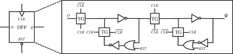
Figure 2.7 DFF with asynchronous reset
One of the possible DFF implementations is also shown in Figure 2.7. The box labeled with TG is called transfer gate that determines the connection of input and output signals of TG depending on two control signals.
When ![]() , Q becomes 0 regardless of the value of
, Q becomes 0 regardless of the value of ![]() , as shown in Figure 2.8. This indicates that the reset signal is effective asynchronously with the clock signal.
, as shown in Figure 2.8. This indicates that the reset signal is effective asynchronously with the clock signal.

Figure 2.8 State of DFF when  (reset is provided)
After the reset is released, that is, ![]() , the state of DFF is determined by
, the state of DFF is determined by ![]() and D. Figure 2.9 shows an example of the state transition when the clock signal changes from
and D. Figure 2.9 shows an example of the state transition when the clock signal changes from ![]() to
to ![]() . Suppose that
. Suppose that ![]() and
and ![]() when
when ![]() . The right-hand side of the DFF circuit has a ring circuit that is composed of only combinatorial logics. Therefore, the output of DFF is fixed as
. The right-hand side of the DFF circuit has a ring circuit that is composed of only combinatorial logics. Therefore, the output of DFF is fixed as ![]() . Note that after the reset,
. Note that after the reset, ![]() .
.

Figure 2.9 State change in DFF for a normal operation, 
As the timing of the ![]() becomes
becomes ![]() , that is, positive edge of the clock, TGs change the states, and the ring circuit is shifted to the left-hand side of the DFF to store the value of
, that is, positive edge of the clock, TGs change the states, and the ring circuit is shifted to the left-hand side of the DFF to store the value of ![]() . Moreover, the value of Q changes from
. Moreover, the value of Q changes from ![]() to
to ![]() . All the signals in the DFF circuits are
. All the signals in the DFF circuits are ![]() or
or ![]() after
after ![]() becomes 1. In other words, the value of D is retrieved and stored in the DFF, and Q is replaced with D.
becomes 1. In other words, the value of D is retrieved and stored in the DFF, and Q is replaced with D.
For example, sequential logics enable us to construct a counter that increments number synchronized with the clock signal. The incrementation timing is at the positive edge of the clock signal if positive-edge-triggered DFFs are used. An 8-bit up counter can be realized with the 8-bit adder, as introduced in Figure 2.5, and the 8-bit DFF.
Figure 2.10 describes the pseudo Verilog code for the 8-bit up counter, and the corresponding timing waveform is shown in Figure 2.11. While the reset is activated, 8-bit DFF is initialized, and hence the output of the 8-bit adder, ![]() , becomes
, becomes ![]() as the adder module increments the input value,
as the adder module increments the input value, ![]() , by one.
, by one.
module up_counter (clk, rst_n, cnt)
   input  clk, rst_n;
   output [7:0] cnt;
   reg [7:0] cnt;
   reg [7:0] cnt_next; // Output of combinatorial logics
   8bit_adder 8add(cnt, 1'b1, cnt_next, Cout);
   always @(posedge clk or negedge rst_n) begin
      if (rst_n == 0)
         cnt <= 0;
      else
         cnt <= cnt_next;
   end
endmodule
Figure 2.10 Pseudo Verilog code for 8-bit up counter
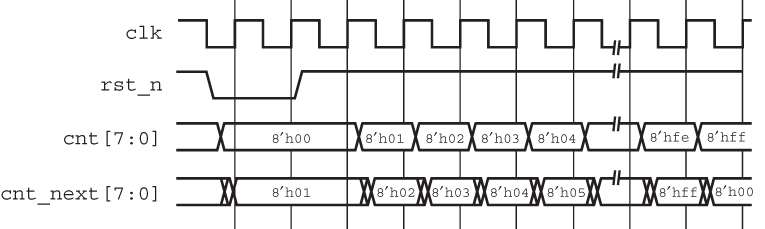
Figure 2.11 Timing waveform for 8-bit up counter
At the timing of the first positive edge of the clock signal, ![]() , after the reset signal,
, after the reset signal, ![]() , is deactivated, 8-bit DFF retrieves the value of
, is deactivated, 8-bit DFF retrieves the value of ![]() , and the output of DFF becomes
, and the output of DFF becomes ![]() . Likewise,
. Likewise, ![]() counts up to
counts up to ![]() using 255 clock cycles after the reset is released, and it becomes
using 255 clock cycles after the reset is released, and it becomes ![]() in the next cycle.
in the next cycle.
2.3.3 Controller and Datapath Modules
2.3.3.1 Finite State Machine as Controller
A controller logic is regarded as finite state machine (FSM) whose next state is determined by the current state and several external conditions. FSM is often described with bubbles and arrows as illustrated in Figure 2.12. The bubble represents the state, and the arrow indicates the state transition. Figure 2.12 is a possible FSM representation for a controller design that controls an encryption of a 10-round block cipher.

Figure 2.12 State machine for an encryption hardware of a 10-round block cipher
Suppose that there are two external conditions, one condition, START, is for starting a cipher operation, that is, encryption, and another condition is RESET that is use for initializing the block cipher hardware. For simplicity, 1-round operation is iteratively performed in a single clock cycle under fixed input variables5 after START. The operation is finished at the 10th round, and the ciphertext is available in the calculation result.
As the cipher operation has to be stopped in 10 cycles, the state, S11, for keeping the result is prepared. If RESET is detected at the state, S11, that is, the corresponding reset signal becomes active, the state goes to the initial state, S0. Note that RESET is different from a hardware reset that is normally provided to reset the entire circuit including FSM and even other modules. Table 2.2 explains the details of FSM. In this case, there exist 12 states in total. The corresponding pseudo Verilog code is shown in Figure 2.13. As the states are realized with sequential logics, at least three DFFs are necessary. Moreover, the state transitions are straightforward from S1 to S11 in this case. That is, there is no legal way to stop the state transitions after START except providing the hardware reset.
Table 2.2 State transitions of FSM shown in Figure 2.8
| External condition | State | Control |
| Hardware reset | ||
| S0 | Initial state | |
| START | S0 | Initial state |
| S1 | Perform 1st-round operation | |
| S2 | Perform 2nd-round operation | |
| ⋮ | ⋮ | |
| S10 | Perform 10th-round operation | |
| S11 | Keep result | |
| RESET | S11 | Keep result |
| S0 | Initial state |
module 10r_enc_fsm (clk, rst_n, START, RESET, state);
   input  clk; rst_n;
   input  START; // Start Encryption
   input  RESET; // Reset FSM
   output [3:0] state;
   reg [3:0] state;
   reg [3:0] next_state;
   always @(posedge clk or negedge rst_n) begin
      if (rst_n == 0)
         state <= 0;
      else
         state <= state_next;
   end
   always @(state or START or RESET) begin
      case (state)
         4'b0000: begin // Initial State
            if (START == 1'b1) next_state = 4'b0001;
            else next_state = 4'b0000;
         end
         4'b0001: // 1st round operation
            next_state = 4'b0010;
         4'b0010: // 2nd round operation
            next_state = 4'b0011;

         4'b1010: // 10th round operation
            next_state = 4'b1011;
         4'b1011: begin // Keep Result
            if (RESET == 1'b1) next_state = 4'b0000;
            else next_state = 4'b1011;
         end
         default:
            next_state = 4'b0000;
      endcase
   end
endmodule
4'b1010: // 10th round operation
next_state = 4'b1011;
4'b1011: begin // Keep Result
if (RESET == 1'b1) next_state = 4'b0000;
else next_state = 4'b1011;
end
default:
next_state = 4'b0000;
endcase
end
endmoduleFigure 2.13 Pseudo Verilog code for FSM for an encryption hardware of a 10-round block cipher
As is often the case with block ciphers, the same operation is performed for each round except a small treatment of the first and last rounds. Suppose that all the rounds use an identical round operation, that is, round operation unit is called iteratively from FSM. In this case, the states, S1–S11, are redundant as they are the states of calling the same round operation. Having a counter unit that counts the number of round operations performed, FSM in Figure 2.14 can be realized with less bubbles.
The advantage of the less bubbles lies not only in the simplicity but in the possibility of choosing any number of rounds. The sequence listed in Table 2.3 is the state transitions for the simplified FSM.
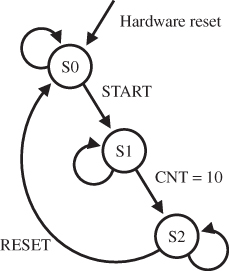
Figure 2.14 Simplified state machine for an encryption hardware of a 10-round block cipher
Table 2.3 State transitions for Figure 2.13
| External condition | State | Control |
| Hardware reset | ||
| S0 | Initial state, CNT = 0 | |
| START | S0 | Initial state |
| S1 | Perform 1st-round operation, and increment CNT | |
| ⋮ | ⋮ | |
| S1 | 10th-round operation, and increment CNT | |
| S2 | Keep result | |
| RESET | S2 | Keep result |
| S0 | Initial state |
The pseudo Verilog code for the combinatorial logics of ![]() can be described as shown in Figure 2.15. The code is configurable with the number of rounds simply by changing the parameter
can be described as shown in Figure 2.15. The code is configurable with the number of rounds simply by changing the parameter ![]() that is defined in the first line of the code.6
that is defined in the first line of the code.6
`define N\_ROUND 10
   always @(state or START or RESET or CNT) begin
      case (state)
         2'b00: begin // Initial State
            if (START == 1'b1) next_state = 2'b01;
            else next_state = 4'b0000;
         end
         2'b01: // 1st to 10th round operations
            if (CNT == N_ROUND) next_state = 2'b10;
            else next_state = 4'b0000;
         end
         2'b10: begin // Keep Result
            if (RESET == 1'b1) next_state = 2'b00;
            else next_state = 2'b10;
         end
         default:
            next_state = 2'b00;
      endcase
   end
Figure 2.15 Pseudo Verilog code for encryption of a 10-round block cipher
2.3.3.2 Datapath
The datapath contains functional units that process data operations, for example, arithmetic addition, modular multiplication, permutation transformation, and so on. On the basis of the orders from FSM, the datapath starts operations with single or multiple inputs depending on the operation. The operation result appears on the output of the datapath after all the signals are evaluated and determined. Note that it takes a fixed amount of time until the operation result is available, which is called path delay.
The operation time should be short enough to guarantee correct operations, that is, the operation result needs to be determined for any input values within the clock period, ![]() , with an appropriate margin, which will be explained later in this chapter. However, some operations such as 64-bit modular multiplication spend more time compared to the case of 8-bit addition, and hence multiple clock cycles may be used until the result is available.
, with an appropriate margin, which will be explained later in this chapter. However, some operations such as 64-bit modular multiplication spend more time compared to the case of 8-bit addition, and hence multiple clock cycles may be used until the result is available.
The path delay of the datapath usually depends on the value change of the inputs. If all the input values to be evaluated in the datapath are completely the same as the previously evaluated ones, all the signals in the datapath never change. In other words, the operation result is available with the operation time zero. Moreover, depending on the functionality of the datapath, there is a case that the input value difference does not effect the output value.7 On the other hand, some change in the input value causes signal changes in the datapath, the so-called signal toggles, and it normally effects the output of the datapath.
2.4 Memory Modules
2.4.1 Single-Port SRAM
A static random access memory (RAM) or SRAM is often used in the modern circuit design. It serves as a local memory that is dedicated to a specific module or as a global memory that can be accessed from multiple modules. SRAM is a significantly important module that allows to store temporary data with the high density as single bit can be stored with six transistors.8
A single-port SRAM has a common address port and it supports read or write operations together with a write enable signal. Owing to its specification, the single-port SRAM is not able to perform read and write operations at the same time. Figure 2.16 shows the timing waveform for a read operation of a typical single-port SRAM that is synchronized with the clock signal. The address data is fetched at the timing of positive edge of the clock signal and checks if the write enabled is high (read) or low (write). SRAM decodes the address data and sets the corresponding data on the data output signals that are controlled by the output enable signal. If the output signal is low, the SRAM data can be observed from the data output after a while, which causes a one-cycle delay as shown in the figure. If the address data is changed in the next cycle, for example, from A to B in the figure, the corresponding data, QB, is output subsequently to QA.9

Figure 2.16 Example for read operation of single-port SRAM
For a write operation, written data and address are fetched at the same timing when the write-enabled signal is detected low at the positive edge of the clock. As shown in Figure 2.17, the write operations can be performed every single cycle.

Figure 2.17 Example for write operation of single-port SRAM
As the read and write operations of single-port SRAM are performed sequentially, bandwidth becomes limited by the bus width of the data signal and the operating clock frequency. In order to overcome the limitation, one can consider the use of multiple ports.
2.4.2 Register File
A register file consists of several registers that are realized based on DFFs or SRAM, for instance. The register file is usually used in central processing unit (CPU) in executing instructions, and hence multiple read ports are required to accelerate a multioperand operation. For instance, the two-operand addition, ![]() , can be performed in a single cycle when using a register file with two read ports and one write port. Such register file is called 2R–1W register file. Hardware modules can choose different types of memory modules depending on different purposes.
, can be performed in a single cycle when using a register file with two read ports and one write port. Such register file is called 2R–1W register file. Hardware modules can choose different types of memory modules depending on different purposes.
Compared to SRAM and DFF, the feature of register file is summarized in Table 2.4.
Table 2.4 Features of SRAM, Register File, and DFF
| Single-port SRAM | Register file | DFF | |
| Bandwidth | Arbitrary | ||
| Shared level | Flexible | Module | Combinatorial logics |
| Memory cost* | Efficient | Medium | Inefficient |
| Memory size | Large | Medium |
Small |
* Depending on the size of memory and available library, register file or even DFF might become more cost efficient than SRAM.
The bandwidth is decided by the bus width and the number of read/write ports in the case of register file, whereas it is proportional to the bus width only in the case of single-port SRAM. The shared level of the single-port SRAM is quite flexible, that is, it can be used in a single or multiple modules as it is cost efficient and is able to support a large size capacity. On the contrary, the register file is normally dedicated to a specific module owing to the limitation as for the cost and size.
2.5 Signal Delay and Timing Analysis
2.5.1 Signal Delay
2.5.1.1 Setup Time and Hold Time
In a basic synchronous design, all signals are retrieved by DFFs at the positive edge of the clock. This is realized by the TGs, which determine the circuit connectivity as explained in Section 2.3.2. Therefore, the input signal D should not be changed at the positive edge of the clock for a stable operation of DFF.
As shown in Figure 2.18, setup time or ![]() is defined by the minimum time period that the data signal has to be determined before the positive edge of the clock signal. On the contrary, hold time or
is defined by the minimum time period that the data signal has to be determined before the positive edge of the clock signal. On the contrary, hold time or ![]() is the minimum time period that the data signal has to be held after the positive edge of the clock signal. The gray-colored parts in the data signal represent the forbidden time of the data change.
is the minimum time period that the data signal has to be held after the positive edge of the clock signal. The gray-colored parts in the data signal represent the forbidden time of the data change.

Figure 2.18 Setup time and hold time
2.5.1.2 Critical Path Delay
A path delay, ![]() , is defined as the time spent for a signal propagation through a path between the input and the output of a combinatorial logic. The critical path delay, denoted as
, is defined as the time spent for a signal propagation through a path between the input and the output of a combinatorial logic. The critical path delay, denoted as ![]() , is a path delay that has the maximum signal transition time among all of the paths in the combinatorial logics. Suppose that a module is implemented with the synchronous-style design method. The following condition must be satisfied in order to satisfy the setup-time requirement.
, is a path delay that has the maximum signal transition time among all of the paths in the combinatorial logics. Suppose that a module is implemented with the synchronous-style design method. The following condition must be satisfied in order to satisfy the setup-time requirement.
Suppose that data is provided to a combinatorial logic at the positive edge of ![]() , and the output of the combinatorial logic is retrieved by DFF whose clock signal is
, and the output of the combinatorial logic is retrieved by DFF whose clock signal is ![]() . The positive edge of
. The positive edge of ![]() arrives to DFF earlier than that of
arrives to DFF earlier than that of ![]() by
by ![]() , whereas the period is the same as
, whereas the period is the same as ![]() . This is the worst condition for the setup-time requirement as for clock skew. In this case, the timing budget for the combinatorial logic is reduced from
. This is the worst condition for the setup-time requirement as for clock skew. In this case, the timing budget for the combinatorial logic is reduced from ![]() to
to ![]() . Moreover, taking the setup margin into consideration, the critical path delay should be
. Moreover, taking the setup margin into consideration, the critical path delay should be ![]() at most.
at most.
That is, the maximum clock frequency, ![]() , for the circuits illustrated on the right-hand side of Figure 2.19 is derived as
, for the circuits illustrated on the right-hand side of Figure 2.19 is derived as

Figure 2.19 Condition for satisfying setup time
As for the hold-time requirement as illustrated in Figure 2.20, the following condition must hold.
where ![]() is the minimum path delay of the combinatorial logic. In this case, it is assumed that the phase
is the minimum path delay of the combinatorial logic. In this case, it is assumed that the phase ![]() is delayed by
is delayed by ![]() to set the worst case for clock skew. Note that the condition does not include
to set the worst case for clock skew. Note that the condition does not include ![]() . This fact indicates that the hold-time requirement should be adjusted by the addition of delay elements, the so-called hold buffer, in the combinatorial circuit if
. This fact indicates that the hold-time requirement should be adjusted by the addition of delay elements, the so-called hold buffer, in the combinatorial circuit if ![]() is too small.
is too small.
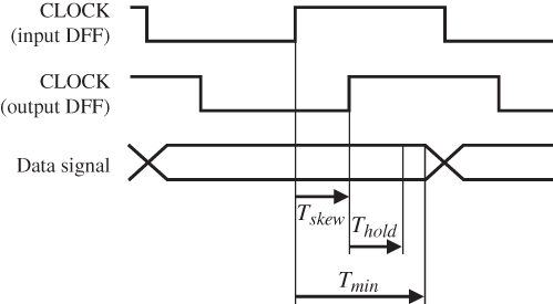
Figure 2.20 Condition for satisfying hold time
Both the setup-time and hold-time conditions introduced here assume the worst case, and hence it may not happen in a real design. In order to increase the maximum clock frequency and to reduce the cost of hold buffers, timing analysis should be performed with a precise timing model.

Figure 2.21 Example of hold buffer
2.5.2 Static Timing Analysis and Dynamic Timing Analysis
2.5.2.1 Timing Analysis without Test Vectors
Once RTL coding is completed, it is synthesized with a library and converted into gate-level netlist so that the behavior of the functional module is represented with bit-wise operations and memory modules including DFF. Therefore, compared to the RTL description, the netlist enables us to evaluate the timing delay of the combinatorial logics much closer. At this moment, designers can perform a rough estimation for the critical timing delay, ![]() , based on the delay model of each gate and wire connecting gates. This analysis method is called static timing analysis (STA) named after the way of estimating the delay. That is, STA does not care for the value in the netlist. The advantage of STA is its fast analysis because any functional simulation with a test vector is not required. However, it sometimes causes an accurate result for the delay estimation. More precisely, the result of STA becomes significantly marginal when evaluating the paths that never happen in reality.
, based on the delay model of each gate and wire connecting gates. This analysis method is called static timing analysis (STA) named after the way of estimating the delay. That is, STA does not care for the value in the netlist. The advantage of STA is its fast analysis because any functional simulation with a test vector is not required. However, it sometimes causes an accurate result for the delay estimation. More precisely, the result of STA becomes significantly marginal when evaluating the paths that never happen in reality.
In order to see this, consider the example case shown in Figure 2.22. Suppose that DFFs provide inputs to a combinatorial logic that is composed of combinatorial logics X and Y, one INV gate and one AND gate. The outputs of DFF_A and DFF_B are connected to the combinatorial logic X. Therefore, at the positive edge of the clock, the gates in the combinatorial logic X start being evaluated. It is assumed that all the signals in the combinatorial logic X are determined in ![]() .
.

Figure 2.22 Example circuit for timing analysis
DFF_C provides the signal s, and it determines the input for the combinatorial logic Y. When ![]() , the combinatorial logic Y takes
, the combinatorial logic Y takes ![]() and the output of DFF_A as inputs. In this case, the path delay is estimated from the path between DFF_C and DFF_D as
and the output of DFF_A as inputs. In this case, the path delay is estimated from the path between DFF_C and DFF_D as ![]() . Here, it is assumed that the path starting from DFF_A is not a critical one.
. Here, it is assumed that the path starting from DFF_A is not a critical one.
On the other hand, in the case of ![]() , the path delay should be evaluated between DFF_B and DFF_D as
, the path delay should be evaluated between DFF_B and DFF_D as ![]() . If the delay of the combinatorial logic X is
. If the delay of the combinatorial logic X is ![]() , the critical path delay is derived from the path delay as
, the critical path delay is derived from the path delay as ![]() . However, it sometimes happens that the signal s never becomes
. However, it sometimes happens that the signal s never becomes ![]() depending on the usage of the design. In this case, the path between DFF_B and DFF_D is regarded as false path. Obvious false paths, such as the case shown in Figure 2.22, can be eliminated easily in STA, but it is quite difficult to find all the false paths in a complicated combinatorial logic.
depending on the usage of the design. In this case, the path between DFF_B and DFF_D is regarded as false path. Obvious false paths, such as the case shown in Figure 2.22, can be eliminated easily in STA, but it is quite difficult to find all the false paths in a complicated combinatorial logic.
2.5.2.2 Timing Analysis with Test Vectors
Timing analysis with test vectors, which is called dynamic timing analysis (DTA), is also used for timing verification. DTA overcomes the major problem of STA as it excludes all of the false paths and focuses only on the true paths of the design. In addition, DTA checks the functionality of the design at the same time. DTA is suitable when the designer can prepare the test vectors such that the critical path is activated. However, DTA has the disadvantage that it requires more analysis time compared to STA. Furthermore, if the prepared test vectors do not activate the critical path, DTA results report a faster clock frequency than what the fabricated chip can work correctly without setup-time errors.
2.6 Cost and Performance of Digital Circuits
2.6.1 Area Cost
Digital circuits are normally implemented on silicon wafer, and occupy some space. Larger space usage results in a higher cost in fabrication as far as the silicon die size is restricted with the circuit area.10 Moreover, the larger circuits tend to consume more power if the gates in the circuits are activated in a constant rate. In this regard, cost of a design circuit can be regarded as the size of the circuit or the gate equivalent by onedefinition.
The size of the circuit can be measured with the actual size, for example, in units of nano square meters (nm![]() ). The gate equivalent is typically calculated by dividing the circuit area by the area of a 2-input NAND gate whose drivability is 1.
). The gate equivalent is typically calculated by dividing the circuit area by the area of a 2-input NAND gate whose drivability is 1.
2.6.2 Latency and Throughput
In the field of digital circuits, performance often means computational speed. In order to improve computational speed, we have several factors to optimize, which are clock frequency used for a digital circuit, the number of clock cycles needed for computation, the amount of data processed in a clock cycle, and so on. Especially, latency and throughput are the two key metrics for performance.
Latency is defined as the response time of computation. Suppose that given computation requires N cycles, the latency, L, can be expressed as
where f is the clock frequency. Note that the number of clock cycles is also used as another indicator of latency.11
Throughput, R, can be derived as
where f is the clock frequency and D the amount of input data processed in a computation. If the amount of data per clock cycle, ![]() , is constant, it is found that the throughput, R, is simply proportional to the clock frequency, f. The alternative view is that the amount of data per clock cycle should be increased in order to improve the throughput under the situation, where the clock frequency cannot be increased.
, is constant, it is found that the throughput, R, is simply proportional to the clock frequency, f. The alternative view is that the amount of data per clock cycle should be increased in order to improve the throughput under the situation, where the clock frequency cannot be increased.
Further Reading
- Ercegovac MD and Lang T 2004 Digital Arithmetic. Morgan Kaufmann Oxford, San Francisco, CA.
- Hennessy JL and Patterson DA 2002 Computer Architecture: A Quantitative Approach 3rd edn. Morgan Kaufmann Publishers Inc., San Francisco, CA.
- (ed. Oklobdzija VG) 2007 Digital Systems and Applications, The Computer Engineering Handbook 2nd edn. CRC Press, Boca Raton, FL.